I. INTRODUCTION
Nanoindentation of materials is the most popular method to determine their mechanical properties at both micro- and nanoscales. The load–displacement curve, the Young's modulus, and the indentation size effect have been widely studied by both experimental and modeling methods (e.g., Refs. Reference Oliver and Pharr1–Reference Haghighi, Lu, Jian, Cao, Habibi and Zhang6). However, most of the studies have focused on discovering the mechanical properties of a single grain by using single-crystal materials or polycrystalline materials due to the fact that the indent is quite small and can be located within a grain of the materials. In polycrystalline materials, two adjoining crystals that are dissimilar in orientation or structure form an interface. The interface formed by two crystals with the same structure but different orientations is often called grain boundary (GB); while the interface formed by two crystals of different lattice structures is called phase boundary (PB).Reference Mayeur, Beyerlein, Bronkhorst and Mourad7 Recently, there has been an increasing concern about the interface effects of polycrystalline materials on their nanoindentation behaviors.
Britton et al.Reference Britton, Randman and Wilkinson8 studied the slip transfer phenomenon at GBs by nanoindentation tests. A pop-in event which is a sudden displacement jump was observed in the loading part of load–displacement curve for body-centered cubic (BCC) materials but not face-centered cubic (FCC) materials. Ohmura et al.Reference Ohmura, Minor, Stach and Morris9 investigated dislocation-GB interactions in martensitic steel through in situ nanoindentation in a transmission electron microscopy (TEM). It was found that the dislocations produced by the indentation were simply absorbed into the boundary, without dislocation pileup or the transmission of strain. Wang and NganReference Wang and Ngan10 found the pop-in phenomenon by doing indentation near GB in niobium. Its occurrence was rationalized in terms of slip transmission across the GB. Wo and NganReference Wo and Ngan11 investigated the influence of GBs on material deformation in Ni3Al by carrying out nanoindentation tests near its GB. They found that hardness is not a sensitive parameter to measure GB strengthening effects. Ohmura et al.Reference Ohmura, Tsuzaki and Yin12 found the same phenomenon by performing the nanoindentation tests in the vicinity of single GB of interstitial-free steel. Lee et al.Reference Lee, Han, Smallman, Feng and Lai13 reported a significant change of hardness close to GB of the Ni3Al bicrystal. However, their results could not be reproduced by other researchers.Reference Wo and Ngan11 A few studies showed that there is a weak dependence of hardness on the distance from the GB when using low maximum loads for hardness measurement.Reference Soifer, Verdyan, Kazakevich and Rabkin14–Reference Soer, Aifantis and De Hosson17 Eliash et al.Reference Eliash, Kazakevich, Semenov and Rabkin18 did a systematic investigation of it and found that the trend vanished when the indentation loads exceeded 10 mN using a Berkovich indenter. Furthermore, Nilsen and SubramanianReference Nilsen and Subramanian19 performed indentation studies on two-phase bicrystals of alpha-beta brass with various geometries of the PB to discover its role in the propagation of deformation. The PB acted as a very effective barrier for slip propagation, irrespective of its geometry.
However, the nanoindentation tests cannot capture the detailed three-dimensional (3D) microstructure information including misorientation map of deformed materials. Thus, 3D crystal plasticity finite element method (CPFEM) simulation has been used to study the nanoindentation behaviors extensively. It is different from the conventional FEM which cannot capture the anisotropy and orientation evolution in crystalline materials during indenting process. The conventional FEM does not contain the constitutive model based on the fact that plastic deformation occurs by crystallographic slipping on slip systems and the rotations of the crystal lattices. Therefore, 3D CPFEM which considers dislocation slips and lattice rotations as the only deformation mechanism plays an important role in investigating mechanical properties of single-crystal and polycrystal materials.
The 3D CPFEM study of the mechanical behavior, microstructure and microtexture evolution for single-crystal materials via nanoindentation modeling was frequently reported for the last decade.Reference Liu, Varghese, Ma, Yoshino, Lu and Komanduri20 Kalidindi et al.Reference Kalidindi, Bronkhorst and Anand21 simulated the load–indentation depth curve of the forging process and the result agrees with that from the experiment. A combination of 3D discrete dislocation simulation and the FEM was developed by Fivel et al.Reference Fivel, Robertson, Canova and Boulanger22 to study the formation of an indent-induced plastic zone during nanoindentation on copper single crystal. The simulated microstructure has been directly compared to that obtained from TEM observations. It showed that both the simulated dislocation microstructure and the corresponding indent-induced plastic volume were quite realistic. Liu et al.Reference Liu, Wang, Yoshino, Roy, Lu and Komanduri23 determined the mesoplastic parameters for CPFEM model by fitting the simulated load–displacement curves to the experimental data and used them to determine the stress–strain relationship of a single-crystal copper at meso-scale. They also conducted the simulations using a commercial finite element code (ABAQUS) with a user-defined subroutine (VUMAT) that incorporates crystal plasticity constitutive model to discuss the orientation effects in nanoindentation of single-crystal copper.Reference Liu, Varghese, Ma, Yoshino, Lu and Komanduri20 Zaafarani et al.Reference Zaafarani, Raabe, Singh, Roters and Zaefferer24 used 3D CPFEM to investigate the texture and microstructure below a nanoindent in a Cu single crystal and compared the results with those from electron backscatter diffraction (EBSD) tests. Although the simulations failed to predict the fine details of the patterning of the rotation directions with the frequent changes in sign observed in the experiment and overemphasize the magnitude of the rotation field tangent to the indenter, they showed a similar pattern for the absolute orientation changes and provided details of the shear distribution in the deformation zone on the different slips systems. Zaafarani et al.Reference Zaafarani, Raabe, Roters and Zaefferer25 also used a CPFEM which is based on a dislocation density-based constitutive model to study the plastic deformation-induced rotation patterns below nanoindents. By comparing to the experiment, it was found that the complex rotation pattern induced during conical indentation was well predicted. Lee and ChenReference Lee and Chen26 observed the size effect in the microindentation of FCC single-crystal copper modeled by the employment of mechanism-based strain gradient crystal plasticity. Recently, EidelReference Eidel27 found experiments and CPFEM simulations were in agreement about predicting pile-up during indentation on the surface of a single crystal material. However, the modeling of nanoindentation behavior with polycrystal materials is much more complicated due to the complex nature of the polycrystals and the challenges in modeling 3D grains. Thus, most of the CPFEM modelings were carried out on either polycrystals in 2D or single crystal in 3D.Reference Li, Shen, Proust, Moy and Ranzi28
Recently, Li et al.Reference Li, Shen, Proust, Moy and Ranzi28 are the first and only group that proposed an approach to study 3D CPFEM simulation of nanoindentation on aluminum alloy. It was found that high angle GBs act as barriers to cause local stress concentrations. However, it contradicted with previous experimental reports indicating there is little resistance to slip transfer across GBs for FCC metals.Reference Britton, Randman and Wilkinson8 Besides, the study only discussed the effects of GB from one-phase FCC metal. Does the grain/phase boundary (GB/PB) affect a one-phase FCC bicrystal and a two-phase FCC bicrystal differently? Do GBs/PBs with different misorientations affect the same material significantly? To answer above questions, the 3D bicrystal CPFEM model has been established to investigate the effects of GBs on nanoindentation behaviors. The Voronoi tessellation method has been used to develop the 3D bicrystal model, which is exactly the same as developing 3D polycrystal. However, comparing to the polycrystal, the bicrystal is able to provide much more details to define the GB/PB. To the best knowledge of authors, it is the first work to simulate the behavior of GB/PB in both one-phase bicrystalline material and two-phase bicrystalline material during nanoindentation deformation through crystal plasticity theory.
II. CONSTITUTIVE MODELS AND FINITE ELEMENT SIMULATIONS
A. Kinematics of crystalline deformation
The quantitative description of kinematical theory for the mechanics of elastic–plastic deformation of crystals is derived from the earlier work done by TaylorReference Taylor29 and Hill.Reference Hill30 It is found that material flows through the crystal lattice via dislocations gliding along the corresponding slip systems. The constitutive models used here follows the earlier works by Asaro,Reference Asaro31 Asaro and RiceReference Asaro and Rice32 and Huynh.Reference Si, Lu, Huynh, Tieu and Liu33–Reference Liu, Lu, Tieu and Yu35
The crystalline material under load undergoes crystallographic slip due to dislocation motion on the active slip systems and elastic deformation including stretching and rotating of the crystal lattice,Reference Asaro31–Reference Si, Lu, Huynh, Tieu and Liu33,Reference Peirce, Asaro and Needleman36,Reference Asaro and Needleman37 which leads to a hypothesis that the crystallographic slipping may be supposed to firstly occur from the reference configuration to the intermediate configuration, followed by the elastic stretching and rotation from the intermediate configuration to the current configuration. Therefore, three configurations have been proposed to describe the deformation process. The initial configuration corresponds to the original undeformed state of the element and the current configuration corresponds to the deformed state of the element. The intermediate configuration is obtained from the current configuration when relaxing the lattice elastic stretching and rotation. The total deformation gradient F can be decomposed into two different components, namely F* and FP as
 $${\bi{F}} = {{\bfi\partial \bi{x}} \over {\bi\partial X}} = {{\bi{F}}^*} \cdot {{\bi{F}}^{\rm{P}}}\quad ,$$
where X represents the position of material points in the reference configuration and x denotes the position of material points in the current configuration. Here, F is the total deformation gradient, F∗ describes the elastic deformation gradient including the stretching and rotation of the crystal lattice, and FP indicates the crystallographic slip on the slip system, which can be written as
 $${{\bi{F}}^{\rm{P}}} = \mathop\sum\limits_{\alpha = 1}^N {{{\bi{F}}^{\left( \alpha \right){\rm{P}}}}} = \mathop\sum\limits_{\alpha = 1}^N {{\bi{I}} + {\gamma ^{\left( \alpha \right)}}\left( {{\bf{s}}_0^{\left( \alpha \right)} \otimes {\bf{m}}_0^{\left( \alpha \right)}} \right)} \quad ,$$
where  ${{\bi{F}}^{\left( \alpha \right){\rm{P}}}}$ is the contribution of the α-th slip system to FP, γ(α) is the shear strain of α-th slip system, ⊗ indicates the dyadic product of two tensors or vectors, I is a second-order unit tensor, and N is the number of activated slip systems. The Green strain tensor can be written as
 $${\bi{E}} = {1 \over 2}\left( {{{\bi{F}}^{\rm{T}}}{\bi{F}} - {\bi{I}}} \right)\quad .$$
In the initial configuration, the crystal slip system α consists of a slip direction vector  ${\bi{s}}_0^{\left( \alpha \right)}$ lying in a slip plane with normal vector of
 ${\bi{m}}_0^{\left( \alpha \right)}$. Both
 ${\bi{s}}_0^{\left( \alpha \right)}$ and
 ${\bi{m}}_0^{\left( \alpha \right)}$ are unit vectors and should satisfy the orthogonal relationship, namely
 $${\bi{s}}_0^{\left( \alpha \right)} \;\cdot\; {\bi{m}}_0^{\left( \alpha \right)} = 0\quad .$$
Both  ${\bi{s}}_0^{\left( \alpha \right)}$ and
 ${\bi{m}}_0^{\left( \alpha \right)}$ will not be changed during crystallographic slip from the initial configuration to the intermediate configuration but converted with the lattice when the lattice is stretched and rotated from the intermediate to the current configuration. The slip direction vector
 ${\bi{s}}_0^{\left( \alpha \right)}$ can be given in the deformed configuration by
 $${{\bi{s}}^{\left( \alpha \right)}} = {{\bi{F}}^{\left( \alpha \right)}} \cdot {\bi{s}}_0^{\left( \alpha \right)} = {{\bi{F}}^*}\left[ {\mathop \sum \limits_{\alpha = 1}^N {\bi{I}} + {\gamma ^{\left( \alpha \right)}}\left( {{\rm\bf{s}}_0^{\left( \alpha \right)} \otimes {\rm\bf{m}}_0^{\left( \alpha \right)}} \right)} \right]{\bi{s}}_0^{\left( \alpha \right)} = {{\bi{F}}^*} \cdot {\bi{s}}_0^{\left( \alpha \right)}\quad ,$$
and the normal to the slip plane  $m_0^{\left( \alpha \right)}$ after deformation can be written as
 $${\bi{m}^{\left( \alpha \right)}} = {{\bi{s}}^{\left( \alpha \right) - 1}} = {\left( {{\bi{F}^*} \cdot {\bi{s}}_0^{\left( \alpha \right)}} \right)^{ - 1}} = {\bi{m}}_0^{\left( \alpha \right)} \cdot {{\bi{F}}^{* - 1}}\quad .$$
It should be noted that  ${s^{\left( \alpha \right)}}$ and
 ${m^{\left( \alpha \right)}}$ are not in general unit vectors but remain orthogonal as
 $${\bi{s}^{\left( \alpha \right)}}\;\cdot\;{\bi{m}^{\left( \alpha \right)}} = 0\quad .$$
In the crystalline coordinate system, for an FCC crystal,  ${s^{({\rm{\alpha }})}}$ and
 ${m^{\left( \alpha \right)}}$ are given by
 $${{\bi{s}}^{\left( {1 - 3} \right)}} = {1 \over {\sqrt 3 }}\left( {1,1,1} \right),{{\bi{s}}^{\left( {4 - 6} \right)}} = {1 \over {\sqrt 3 }}\left( { - 1,1,1} \right),{{\bi{s}}^{\left( {7 - 9} \right)}} = {1 \over {\sqrt 3 }}\left( {1, - 1,1} \right),{{\bi{s}}^{\left( {10 - 12} \right)}} = {1 \over {\sqrt 3 }}\left( {1,1, - 1} \right)\quad ,$$
 $$\eqalignb{ & {{\bi{m}}^{\left( 1 \right)}} = {1 \over {\sqrt 2 }}\left( {0, - 1,1} \right),{{\bi{m}}^{\left( 2 \right)}} = {1 \over {\sqrt 2 }}\left( {1,0, - 1} \right),{{\bi{m}}^{\left( 3 \right)}} = {1 \over {\sqrt 2 }}\left( { - 1,1,0} \right),{{\bi{m}}^{\left( 4 \right)}} = {1 \over {\sqrt 2 }}\left( {1,0,1} \right)\quad , \cr & {{\bi{m}}^{\left( 5 \right)}} = {1 \over {\sqrt 2 }}\left( {1,1,0} \right),{{\bi{m}}^{\left( 6 \right)}} = {1 \over {\sqrt 2 }}\left( {0, - 1,1} \right),{{\bi{m}}^{\left( 7 \right)}} = {1 \over {\sqrt 2 }}\left( {0,1,1} \right),{{\bi{m}}^{\left( 8 \right)}} = {1 \over {\sqrt 2 }}\left( {1,1,0} \right)\quad , \cr & {{\bi{m}}^{\left( 9 \right)}} = {1 \over {\sqrt 2 }}\left( {1,0, - 1} \right),{{\bi{m}}^{\left( {10} \right)}} = {1 \over {\sqrt 2 }}\left( {0,1,1} \right),{{\bi{m}}^{\left( {11} \right)}} = {1 \over {\sqrt 2 }}\left( {1,0,1} \right),{{\bi{m}}^{\left( {12} \right)}} = {1 \over {\sqrt 2 }}\left( { - 1,1,0} \right)\quad . \cr}$$
The velocity gradient L can be uniquely decomposed into a symmetric part D (stretching rate tensor) and a skew-symmetric Ω (spin tensor) part as
 $${\bi{L}} = {\bi{D}} + \iOmega \quad ,$$
 $${\bi{D}} = {1 \over 2}\left( {\bi{L} + {\bi{L}^{\rm{T}}}} \right)\quad ,$$
 $$\iOmega = {1 \over 2}\left( {\bi{L} - {\bi{L}^{\rm{T}}}} \right)\quad ,$$
where D is, in general, called the rate of deformation. Both tensors D and Ω can also be decomposed into the elastic stretching and lattice rotation component (D* and Ω*) and the plastic component (DP and Ω P) as follows,
 $${\bi{D}} = {\bi{D}^*} + {\bi{D}^{\rm{P}}}\quad ,$$
 $$\iOmega = {\iOmega ^*} + {\iOmega ^{\it{P}}}\quad ,$$
and the tensor DP in Eq. (13) can be expressed as
 $${\bi{D}^{\rm{P}}} = {1 \over 2}\left( {{\bi{L}^{\rm{P}}} + {\bi{L}^{{{\rm{P}}^{\rm{T}}}}}} \right) = \mathop\sum\limits_{\alpha = 1}^N {{\bi{p}^{\left( \alpha \right)}}{{\dot \igamma }^{\left( \ialpha \right)}}} \quad ,$$
where p(α) can be defined as
 $${\bi{p}^{\left( \alpha \right)}} = {1 \over 2}\left( {{\bi{s}^{\left( \alpha \right)}} \otimes {\bi{m}^{\left( \alpha \right)}} + {\bi{m}^{\left( \alpha \right)}} \otimes {\bi{s}^{\left( \alpha \right)}}} \right)\quad .$$
Similar to DP, the tensor Ω P in Eq. (14) can be expressed as
 $${\iOmega ^{\it{P}}} = \mathop\sum\limits_{\alpha = 1}^N {{\bi{w}^{\left( \alpha \right)}}{{\dot \igamma }^{\left( \ialpha \right)}}} \quad ,$$
where q(α) can be defined as
 $${\bi{w}^{\left( \alpha \right)}} = {1 \over 2}\left( {{\bi{s}^{\left( \alpha \right)}} \otimes {\bi{m}^{\left( \alpha \right)}} - {\bi{m}^{\left( \alpha \right)}} \otimes {\bi{s}^{\left( \alpha \right)}}} \right)\quad ,$$
where  ${{\bi{s}}^{\left( \alpha \right)}} \otimes {{\bi{m}}^{\left( \alpha \right)}}$ is the Schmid factor. Here, p(α) and w(α) are symmetric and asymmetric part of the Schmid factor, respectively.
B. Rate-dependent hardening model
The crystal plasticity constitutive model used in this study follows the line described by AsaroReference Asaro31 and it is incorporated into the implicit finite element code ABAQUS/Standard through the user material subroutine (UMAT). The prominent functions of UMAT are to provide the material with the Jacobian matrix for the constitutive model, and to update the stresses and the solution dependent state variables. In this study, we adopt the UMAT framework initially developed by HuangReference Huang38 and use the formulations established by Bassani and WuReference Bassani and Wu39 as the hardening model, which has been specifically described by Liu et al. and Lu et al.Reference Liu, Lu, Tieu and Yu35,Reference Lu, Deng, Tieu, Su, Zhu and Liu40 The formulations of the rate-dependent hardening model used in the present study can be expressed as
 $${\dot \igamma ^{\left( \ialpha \right)}} = \dot \gamma _0^{\left( \alpha \right)}{\mathop{\rm sgn}} \left( {{\itau ^{\left( \ialpha \right)}}} \right){\left| {{{{\itau ^{\left( \ialpha \right)}}} \over {\itau _{\it{c}}^{\left( \ialpha \right)}}}} \right|^{\rm{n}}}\quad ,$$
with
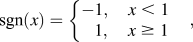 $${\mathop{\rm sgn}} \left( x \right) = \left\{ {\matrix{ {\! - 1,\quad x\; \lt\; 1} \cr \;\;{1,\quad x \;\ge\; 1} \cr} } \right.\quad ,$$
where  $\dot \gamma _0^{\left( \alpha \right)}$ is the reference (initial) value of the shear strain rate, which is a constant for all the slip systems. Here, n is the strain rate sensitive exponent. Both
 $\dot \gamma _0^{\left( \alpha \right)}$ and n are the material parameters. Here,
 $\tau _{\rm{c}}^{\left( \alpha \right)}$ is the critical resolved shear stress of the slip system α, which represents the strength of the material.
The rate of change of the critical resolved shear stress is expressed byReference Hill30
 $${\dot \itau _{\it{c}}}^{\left( \ialpha \right)} = \mathop\sum\limits_{\beta = 1}^N {{f_{\alpha \beta }}{h_{\alpha \beta }}{{\dot \igamma }^{\left( \ibeta \right)}}} \quad ,$$
 $${h_{\alpha \alpha }} = \left[ {\left( {{{\rm{h}}_0} - {{\rm{h}}_{\rm{s}}}} \right)\sec {h^2}\left( {{{\left( {{h_0} - {h_{\rm{s}}}} \right){\igamma ^{\left( \ialpha \right)}}} \over {{\tau _1} - {\tau _0}}}} \right) + {h_{\rm{s}}}} \right]\left[ {1 + \mathop \sum \limits_{\matrix{ {\beta = 1} \cr {\beta \ne \alpha } \cr} }^N {f_{\alpha \beta }}\tanh \left( {{{{\igamma ^{\left( \ibeta \right)}}} \over {{\gamma _0}}}} \right)} \right],\quad {\rm{for}}\,\alpha = \beta \quad ,$$
 $${h_{{\rm{\alpha \beta }}}} = q{h_{\alpha \alpha }},\quad {\rm{for}}\;\alpha \ne \beta \quad ,$$
where h αβ is the hardening modulus including the self-hardening of each system (α = β) and latent hardening (α ≠ β), the constant q is the latent hardening parameter, the constant γ0 is the reference value of slip, γ is the shear strain, τ0 is the initial critical resolved shear stress, τ1 is the breakthrough stress where large plastic flow initiates, h 0 is the hardening modulus just after initial yield, h s is the hardening modulus during easy glide, and f αβ is the magnitude of the strength of a particular slip interaction between two slip systems α and β. The factor f αβ depends on the geometric relation between two slip systems. There are five constants for f αβ, namely α1 (no junction), α2 (Hirth lock), α3 (coplanar junction), α4 (glissile junction), and α5 (sessile junction).
C. Finite element implementation
The aforementioned crystal plasticity constitutive model is implemented into the implicit finite element code ABAQUS/Standard by using the UMAT which are able to provide the material Jacobian matrix  ${{\partial \Delta \sigma } \mathord{\left{\vphantom {{\partial \Delta \sigma } {\partial \Delta \varepsilon }}} \right\kern-\nulldelimiterspace}/ {\partial \Delta \varepsilon }}$, for the constitutive model and to update the stresses and the solution dependent state variables.
The commercial software Abaqus6.9, Pro/ENGINEER Wildfire 4.0, and CUBIT 13.1 have been used to simulate the deformation procedure of nanoindentation. A 3D model has been built to describe the behavior of nanoindentation, which is shown as Fig. 1. The Voronoi diagram is the most popular method to generate polycrystalline material structureReference Zhu, Thorpe and Windle41 in the present. In this study, the 3D Voronoi diagram has been used to generate two 3D cells. Firstly, the input file of 3D nanoindentation setup was generated by Abaqus6.9. Secondly, the input file was implemented into a MATLAB program to construct two 3D cells (grains). Each Voronoi cell corresponds to one seed and the number of seeds will be controlled to determine the average size of the cells. The generated two Voronoi cells are then assigned with different crystallographic orientations and implemented into the CPFEM model. In the CPFEM simulation, each Voronoi cell represents a virtual grain. The detailed description for constructing poly-crystal CPFEM model has been given in our earlier work.Reference Huynh34
3D nanoindentation model setup: (a) the whole model; (b) the upper surface of Cu single crystal; (c) the upper surface of Cu bicrystals (or Cu–Al bicrystals) and (d) through thickness view of Cu bicrystals (or Cu–Al bicrystals).
The indenter is a Berkovich indenter with a 200 nm radius round tip. 13,024 eight-node brick elements and 14,463 nodes with reduced integration (element id: C3D8R) are used in the CPFEM model. A refined mesh is generated in the contact area [Figs. 1(b) and 1(c)] directly underneath the indenter to obtain the accurate contact solution while a coarser mesh is created in the rest region to decrease the elements number in the model and to keep the computer time within limits. The importance of having an appropriate mesh density in the contact area has been proposed by Liu et al.Reference Liu, Varghese, Ma, Yoshino, Lu and Komanduri20,Reference Liu, Wang, Yoshino, Roy, Lu and Komanduri23 The size of the smallest element is about 0.1 μm in all three directions.
The X, Y, and Z coordinates represent the rolling direction, transverse direction, and normal direction, respectively. In this model, the specific Goss orientation is set as the initial orientations, namely the (011) slip plane parallels to the Z axis, and the [100] slip direction parallels to the X axis, to validate the model by comparing the numerical result with the experimental observation. Figure 1(c) shows the upper surface of the sample for Cu bicrystal or Cu–Al bicrystal. For Cu bicrystals, the orientations of Grain 2 are always set as Goss orientations while the orientations of Grain 1 are set as Cube, Brass and R, respectively. For a Cu–Al bicrystal, Grain 2 is set as Cu and its orientations are always set as Goss orientations. Grain 1 is set as Al and its orientations are set as Cube, Brass and R, respectively. The misorientation between Grain 1 and Grain 2 for both Cu bicrystals and Cu–Al bicrystals is listed in Table I. Clearly, all the GBs between Grain 1 and Grain 2 are high angle GBs.
Misorientations for Cu bicrystal and Cu–Al bicrystal between Grain 1 and Grain 2.
The dimensions of the sample in the FEM model are 60 µm × 60 µm × 30 µm. The height of the sample is much larger than the maximum indentation depth (1 µm) to avoid the influence from the sample.Reference Fischer-Cripps42 In addition, the length and the width are bigger enough as the stress contour never reaches four surrounding surfaces of the sample.
All nodes on the bottom surface and four surrounding surfaces of sample are constrained along three axes considering the real indentation condition (the metal sample was mounted inside a piece of resin and just the top surface is free). Liu et al.Reference Liu, Wang, Yoshino, Roy, Lu and Komanduri23 found that both the indentation depth and the load–displacement curve are not affected by the coefficient of friction. Therefore, a frictionless contact pair is defined by two contact surfaces with associated nodes between the indenter and sample. The time step increment is set for the convergence of modeling. In this study, a fixed time step increment 0.01 s is chosen and a total time step increments of 24,062 in the simulation are used, including contact, loading, and unloading.
According to the report from Bassani et al.Reference Wu, Bassani and Laird43 and Huang,Reference Huang38 the factor f αβ for single-crystal copper is taken as: α1 = α2 = α3 = 8, α4 = 15 and α5 = 20 in this study. Three elastic moduli can be used as C11 = 168,400 MPa, C12 = 121,400 MPa, and C44 = 75,400 MPa, respectively.Reference Wu, Bassani and Laird43 Other material parameters in the hardening models (Eqs. 19–22) are listed in Table II.Reference Wu, Bassani and Laird43,Reference Liu, Lu and Tieu44 Franciosi et al.Reference Franciosi, Berveiller and Zaoui45 and Lu et al.Reference Lu, Deng, Tieu, Su, Zhu and Liu40 have reported that the factor f αβ for aluminum can be chosen as: α1 = α2 = α3 = 1.75, α4 = 2 and α5 = 2.25. Other material parameters in the hardening models are listed in the Table III.Reference Liu, Lu, Tieu and Yu35,Reference Lu, Deng, Tieu, Su, Zhu and Liu40 All of these parameters were evaluated by fitting the simulated stress–strain curve with the experimental results of single-crystal aluminum under plane strain compression.Reference Liu, Maurice, Driver and Hansen46,Reference Akef, Fortunier, Driver and Watanabe47 Aluminum has an FCC structure with elastic moduli C11 = 112,000 MPa, C12 = 66,000 MPa, and C44 = 28,000 MPa. There is only one set of slip systems for FCC metals, {111} $\left\langle {110} \right\rangle$, which includes 12 different slip systems shown in the Table IV. In the deformed single-crystal copper and aluminum, slips occur on the {111} planes and in the
 $\left\langle {110} \right\rangle$ directions. All of aforementioned parameters for copper were evaluated by both experiments and simulationsReference Huang38,Reference Casals, Ocenasek and Alcala48,Reference Alcala, Casals and Ocenasek49 and all parameters for aluminum were validated in the simulations of nanoindentation, rolling, tensile, and ECAP deformation.Reference Si, Lu, Huynh, Tieu and Liu33,Reference Liu, Lu, Tieu and Yu35,Reference Lu, Deng, Tieu, Su, Zhu and Liu40,Reference Huynh, Lu, Si and Tieu50,Reference Liu, Tieu, Lu, Zhu and Deng51
Parameters in the constitutive model for copper.Reference Wu, Bassani and Laird43,Reference Liu, Lu and Tieu44

Parameters in the constitutive model for aluminum.Reference Liu, Lu, Tieu and Yu35,Reference Lu, Deng, Tieu, Su, Zhu and Liu40

Notation of the slip systems for the FCC materials considered in this study.

III. RESULTS AND DISCUSSIONS
Figure 2(a) shows the comparison between numerical and experimental load–indentation depth curves.Reference Wei, Wang and Zhao52 The depth controlled modeling has been carried out to achieve the same maximum depth (1000 nm) as the experiment.Reference Wei, Wang and Zhao52 The maximum load in our simulation is 26.08 mN, while it is 26.28 mN in the experiment. Clearly, the simulated result is in a reasonable agreement with that from the experiment.Reference Wei, Wang and Zhao52 It is noteworthy that all the initial condition of simulation is the same as that of experiment, including the same Goss orientation for indented sample, the same indented sample (Cu single crystal) and the same indenter (Berkovich indenter). Figure 2(b) shows the comparison of load–indentation depth curves between the Cu single crystal and Cu bicrystals. Clearly, there are only slight differences between the Cu single crystal and Cu bicrystals, which suggest that the GB affects the load–indentation depth curves of the one-phase material insignificantly. The result is consistent with the work done by Li et al.Reference Li, Shen, Proust, Moy and Ranzi28 who investigated the nanoindentation behavior by 3D CPFEM simulation of polycrystal aluminum. Figure 2(c) shows the comparison of load–indentation depth curves between the Cu single crystal and Cu–Al bicrystals. Clearly, there is a significant difference between the Cu single crystal and Cu–Al bicrystals although all of these indents locate in the grain of Cu. It suggests that the PB affects the mechanical behavior of nanoindentation significantly. The present study agrees with the observations by Nilsen and SubramanianReference Nilsen and Subramanian19 who performed indentation tests on two-phase bicrystals of alpha-beta brass with various geometries of PB. Besides, Fig. 2(c) also shows that the difference in misorientation between the Cu grain and the Al grain does not affect the load–indentation depth curves significantly.
Comparisons of load–displacement curves between: (a) numerical and experimental results for Cu single crystal; (b) the Cu single crystal and Cu bicrystals via simulation and (c) the Cu single crystal and Cu–Al bicrystals via simulation.
The simulated elastic modulus E s along indented surface normal can be calculated via the Oliver–Pharr (O & P) methodReference Oliver and Pharr1:
 $${h_{\rm{c}}} = {h_{{\rm{max}}}} - {\rm{k}}{{{P_{{\rm{max}}}}} \over S},{\rm{k}} = 0.75,S = {\left( {{{{\rm{d}}P} \over {{\rm{d}}h}}} \right)_{h = {h_{{\rm{max}}}}}}\quad ,$$
where P is the indentation load at the maximum load and h is the indentation depth at the maximum load. Here, h c represents the contact depth. The factor k depends upon the indenter. For the Berkovich indenter, the factor k is equal to 0.75, while k = 0.72 is for the conical indenter. Here, S is the slope of the unloading curve. The elastic modulus was determined byReference Oliver and Pharr1
 $${1 \over {{E_{\rm{r}}}}} = {{1 - \inu _{\rm{s}}^2} \over {{E_{\rm{s}}}}} + {{1 - \inu _{\rm{i}}^2} \over {{E_{\rm{i}}}}}\quad ,$$
where E i, E s, νi and νs are Young's modulus and Poisson's ration of the indenter and the sample, respectively. For a diamond, the variables E i and νi are taken to be 1141 GPa and 0.07 (Ref. Reference Oliver and Pharr1). However, in this study, these two parameters can be ignored as the simulated Berkovich indenter is a rigid body.
The slope of unloading curves is used to calculate E r of the indented material:
 $${E_{\rm{r}}} = {{\sqrt \pi } \over 2}{S \over {\sqrt {{A_{\rm{c}}}} }},\;{A_{\rm{c}}} = 3\sqrt 3 {h_{\rm{c}}}^2{\,\tan ^2}\,65.3 = 24.56{h_{\rm{c}}}^2\quad ,$$
where A c is the contact area.
For the materials which are elastically anisotropic, Vlassak and NixReference Vlassak and Nix53,Reference Vlassak and Nix54 demonstrated that relationships in Eqs. (24) and (25) still worked and the reduced modulus could be re-defined as
 $${1 \over {{E_{\rm{r}}}}} = {1 \over E} + {{1 - \nu _{\rm{i}}^2} \over {{E_{\rm{i}}}}}\quad ,$$
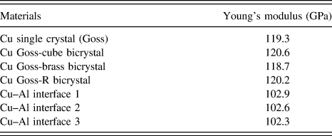
here, the variable E is the theoretical elastic modulus, which is proved to be a complicated function of single-crystal elastic constants C11, C12, and C44. It is also defined as indentation modulus by Wang and Lu.Reference Wang and Lu55 The simulated Young's moduli for Cu samples and Cu–Al bicrystals have been calculated and shown in the Table V. Clearly, the GB does not affect indentation Young's modulus of single-phase material significantly as the maximum difference between the Cu single crystal and Cu bicrystals is only ∼1.09%. However, the maximum difference between the Cu single crystal and Cu–Al bicrystals is ∼16.6%, which suggests that the PB affects indentation Young's modulus significantly.
Simulated Young's modulus for Cu samples and Cu–Al bicrystals.
Figure 3 shows the distributions of the Mises stress on the upper surfaces of Cu samples. The maximum difference in the maximum Mises stress between the Cu single crystal and the Cu bicrystal with Goss-Brass GB is only 3.53%. The difference between the Cu single crystal and Cu bicrystals is insignificant, which suggests that the GB does not become a barrier to block the plastic slip behavior. The former research revealed that there is little dislocation locking and little resistance to slip transfer across GBs for copper.Reference Britton, Randman and Wilkinson8 Soer and De HossonReference Soer and De Hosson56 concluded that slip transmission is unlikely to be observed directly during indentation tests of FCC metals.
The distributions of the Mises stress on the upper surfaces of Cu samples: (a) the Cu single crystal with Goss orientation; (b) the Cu bicrystal with Goss-Cube GB; (c) the Cu bicrystal with Goss-Brass GB and (d) the Cu bicrystal with Goss-R GB.
Figure 4 shows the distributions of Mises stress on the upper surfaces of Cu samples and Cu–Al bicrystals. For Figs. 4(b)–4(d), there is a noticeable dividing line on each upper surface and the Mises stress stops propagates there. The maximum difference in the maximum Mises stress between the Cu single crystal and Cu–Al bicrystals is 10.1%, approximately. Clearly, the PB works like a barrier which can resist the propagation of the Mises stress. It is consistent with the observations from Nilsen and SubramanianReference Nilsen and Subramanian19 who demonstrated that it is not easy to propagate slip through the PB by localized stress caused by indentation.
The distributions of the Mises stress on the upper surfaces of Cu and Cu–Al bicrystals: (a) the Cu single crystal with Goss orientation; (b) the Cu–Al bicrystal with Goss-Cube PB; (c) the Cu–Al bicrystal with Goss-Brass PB and (d) the Cu–Al bicrystal with Goss-R PB.
Figure 5 shows the distributions of the Mises stress on through thickness cross section of Cu samples and Cu–Al bicrystals. Figure 5(a) displays a symmetrical distribution of the Mises stress on the through thickness cross section of the Cu single crystal under the Berkovich indenter. Figure 5(b) shows that the pattern of the stress distribution is similar as Fig. 5(a). However, the pattern is not symmetrical at the vicinity of GB. Figure 5(c) shows that the pattern of the stress distribution is significantly different from Figs. 5(a) and 5(b) as the propagation of the Mises stress is completely resisted by PB, at where the diving line is quite noticeable.
The distributions of the Mises stress on the through thickness cross section of Cu samples and Cu–Al bicrystals: (a) the Cu single crystal with Goss orientation; (b) the Cu bicrystal with Goss-R PB and (c) the Cu–Al bicrystal with Goss-R PB.
Figure 6(a) shows the distribution of pile-up patterns on the upper surface of the Cu single crystal with a two-fold symmetry at the maximum indentation depth. It is consistent with the numerical and experimental observations from Wang et al.Reference Wang, Raabe, Kluber and Roters57 and Hollatz et al.Reference Hollatz, Bobeth, Pompe and Marx58 for Cu and NiAl single crystal on (011) oriented surfaces. Figures 6(b) and 6(c) show that pile-up patterns have been slightly changed due to the effect of GBs. However, the material still flows through the GB. Figure 7 shows the through thickness view of pile-up patterns at the maximum indentation depth.
The pile-up patterns made on the upper surfaces of Cu samples: (a) the Cu single crystal with Goss orientation; (b) the Cu bicrystal with Goss-Cube GB; (c) the Cu bicrystal with Goss-Brass GB and (d) the Cu bicrystal with Goss-R GB.
The pile-up patterns made on the through thickness cross section of Cu samples: (a) the Cu single crystal with Goss orientation; (b) the Cu bicrystal with Goss-Cube GB; (c) the Cu bicrystal with Goss-Brass GB and (d) the Cu bicrystal with Goss-R GB.
Figure 8 shows the comparison of pile-up between Cu–Al bicrystals and the Cu single crystal at the maximum indentation depth. Clearly, the pile-up patterns are significantly changed on the Cu–Al bicrystals due to the blocking of material flow by PB. Figure 9 shows the through thickness view of pile-up patterns at the maximum indentation depth.
The pile-up patterns made on the upper surfaces of Cu single crystal and Cu–Al bicrystals: (a) the Cu single crystal with Goss orientation; (b) the Cu–Al bicrystal with Goss-Cube PB; (c) the Cu–Al bicrystal with Goss-Brass PB and (d) the Cu–Al bicrystal with Goss-R PB.
The pile-up patterns made on the through thickness cross section of Cu single crystal and Cu–Al bicrystals: (a) the Cu single crystal with Goss orientation; (b) the Cu–Al bicrystal with Goss-Cube PB; (c) the Cu–Al bicrystal with Goss-Brass PB and (d) the Cu–Al bicrystal with Goss-R PB.
To analyze the effect of interface on the evolution in the crystallographic orientation during the indentation process, the “misorientation” of each node relative to the initial orientation is partitioned into three components representing the rotation angles around the X (RD), Y (TD), and Z (ND) axes, individually. This method was initially proposed by Wert et al.Reference Wert, Liu and Hansen59 In this study, the contour map of the crystallographic rotation angle around the Y axis is investigated for the cross section along the X axis of three individual indented samples, since the GB/PB is noticeable on the chosen through thickness cross section [refer to Fig. 1(d)]. Positive values represent counter-clockwise rotation and negative values represent the clockwise rotation.
Figure 10 shows the lattice rotation angles for the Cu single crystal, the Cu bicrystal with Goss-Brass GB and the Cu–Al bicrystal with Goss-Brass PB, respectively. For the Cu single crystal, lattices on the left-hand side of the indent rotate clockwise while the ones on the right-hand side rotate oppositely. The rotation angles on both sides of indent are opposite to make the whole sample remain stable. However, for the Cu bicrystal, lattices on the left-hand side of the indent change the rotation direction. It is because that the GB works like a barrier to turn around the lattice rotation angle even the material can flows through it. The lattices which are far away from the indent rotate counter-clockwise to remain the whole sample stable. The Cu–Al bicrystal has the same tendency as the Cu bicrystal, which suggests that the PB has the same effect on the lattice rotation angle as GB does.
Distribution of lattice rotation angles induced by nanoindentation for: (a) the Cu single crystal with Goss orientation; (b) the Cu bicrystal with Goss-Cube GB and (c) the Cu–Al bicrystal with Goss-Cube PB.
IV. CONCLUSIONS
(1) A CPFEM model combined with Bassani and Wu hardening law has been developed to investigate the nanoindentation behavior of Cu bicrystals and Cu–Al bicrystals with three different misorientations. The simulated load–displacement curve for the Cu single crystal with Goss initial orientation has been analyzed and compared with the result from the experiment to validate the parameters.
(2) The numerical results indicate that the interface does not affect the load–displacement curves of Cu bicrystals. However, it affects the load–displacement curves of Cu–Al bicrystals significantly. The effect on load–displacement curves from GBs/PBs with different misorientations is insignificant for both Cu bicrystals and Cu–Al bicrystals.
(3) The GB does not affect indentation Young's moduli of Cu bicrystals significantly as the maximum difference between the Cu single crystal and Cu bicrystal is only ∼1.09%. However, the maximum difference between the Cu single crystal and Cu–Al bicrystal is ∼16.6%, which suggests that the PB affects indentation Young's modulus of the Cu–Al bicrystal significantly.
(4) The maximum difference in the maximum Mises stress between Cu single crystal and Cu bicrystal with Goss-Brass GB is only 3.53%, which suggests that the GB does not block the plastic slip behavior as a barrier. However, the maximum difference in the maximum Mises stress between Cu single crystal and Cu–Al bicrystal is 10.1%, approximately. Clearly, the PB can resist the propagation of the Mises stress in Cu–Al bicrystals.
(5) The pile-up patterns have been slightly changed due to the effect of GB for the Cu bicrystals without blocking of the material flow. The pile-up patterns are significantly changed on the surfaces of Cu–Al bicrystals due to the blocking of the material flow by PB.
(6) The lattice rotation angles under the indent can be turned around by the GBs/PBs for both Cu bicrystals and Cu–Al bicrystals.
ACKNOWLEDGMENTS
The authors acknowledge the financial support from an Australia Research Council Discovery Grant (DP0773329).