I. INTRODUCTION
Organic light-emitting diodes (OLEDs) are a highly promising information display technology. Recently, tremendous progress has been made toward application of OLEDs in full color flat panel displays and other devices. However, with current technologies, OLEDs are still struggling with manufacturing costs that limit the size of OLED panels and with lifetime, especially differential aging of colors. In addition to the cost, there is still much development needed to make OLED displays truly flexible. Our goal is to create a display that is light weight, flexible, thin, extremely low cost, video capable, and provides brilliant color with low power consumption. We believe that roll-to-roll (R2R) manufacturing on plastic substrates will be the key to enabling this goal. Of course, a lot of components are required for fabricating a flexible OLED display. Hewlett–Packard Labs have developed the self-aligned imprint lithography methodReference Mei, Perlov, Jeans and Taussig1 so as to be the first to demonstrate low-cost fabrication of an amorphous silicon thin film transistor (TFT) backplane with submicron resolution and high aspect ratio with a fully R2R process. This has been accomplished on 50-μm-thick, 1-km-long plastic rolls. To be compatible with our highly flexible manufactured TFT backplanes, solution processing is very attractive for fabrication of the OLED frontplane due to its simplicity and highly reduced equipment costs relative to vacuum deposition of small molecules. Vacuum deposition production costs increase superlinearly with the area to be coated, especially for most advanced OLEDs using multilayer structures.Reference Müllen and Scherf2–Reference Kiebooms, Menon, Lee and Nalwa6
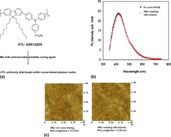
One of the important issues related to solution processing is multilayer capability. Therefore, it is of crucial importance that previously deposited layers are resistant to the solvents used to deposit subsequent layers. Two different approaches are currently applied to such device fabrication: (i) use of “orthogonal” solvents and a change in the polarity/solubility of the materials and (ii) introduction of reactive moieties. However, these approaches have their limitations, such as limited solvent selection or synthetic compatibility, and complication. Our approach is to develop a general method to create semi-interpenetrating polymer network (semi-IPNs) that contain an inert, low-cost polymer network and conjugated conducting polymers serving different purposes in OLED stacks. Our first development, embedding a hole transport material (HTM) into an inert cross-linked polymer network to protect the HTM while processing the subsequent layer, has been reported.Reference Zhou, Sheng, Nauka, Zhao, Gibson, Lam, Yang, Brug and Elder7, Reference Zhou, Sheng, Zhao, Gibson, Lam, Nauka and Brug8 We used ADS132GE, whose structure is shown in Fig. 1(a), as the HTM. It is semi-interpenetrated into a cross-linked polymer network to form semi-IPNs. This cross-linked polymer network mostly preserved the desired optical and electrical properties of the HTM and maintains the morphology of the embedded polymer film even after washing with the solvent that is used for additional layer deposition. This is verified by the corresponding photoluminescence (PL) measurements and atomic force microscopy images shown in Figs. 1(b) and 1(c). A number of OLED devices were fabricated and tested using HTM semi-IPNs as a hole transport layer (HTL) with a subsequent layer of poly(9,9-dioctylfluorenyl-2,7-diyl) (PFO; ADS129BE) as the emissive layer (EML) in the OLED stack. Advantages offered by this HTL included a greatly improved electroluminescence (EL) efficiency and a significant reduction of leakage current by more balanced electron and hole injection in the devices, clearly demonstrating the effectiveness of HTM semi-IPNs.Reference Zhou, Sheng, Zhao, Gibson, Lam, Nauka and Brug8
(a) Scheme of hole transport material semi-interpenetrating polymer networks (HTM semi-IPNs) synthesis; (b) photoluminescence (PL) spectra of HTM semi-IPNs before and after solvent washing; (c) atomic force microscopy images of HTM semi-IPNs.

Inspired by these research findings, this technique has now been expanded to the preparation of emissive semi-IPNs (referred as E-semi-IPN below) containing emissive conjugated conductive polymers and inert polymer networks, which can be easily incorporated into solution-processed multilayer OLED devices. Due to the nature of interpenetrating polymer networks in which polymer networks are at least partially interlaced on a molecular scale, the conductive polymer(s) included in these E-semi-IPNs can be protected from subsequent layer depositions where a solvent would otherwise attack the unprotected underlying film. In addition, the formation of these E-semi-IPNs avoids the complexity of introducing reactive moieties to OLED materials. The results included in this article demonstrate that this synthetic method, with its broad choices of monomers, cross-linkers, and semiconducting polymers for making the suitable semi-IPNs, provides great opportunities to incorporate state-of-the-art emissive polymeric material to achieve red–green–blue (RGB) and white OLEDs. In addition to fabricating bottom-emitting devices, these materials are suitable for manufacturing top-emitting device structures that are more easily integrated onto flexible R2R printed backplanes.
In addition to cost, another challenge facing OLEDs is differential aging of colors. Organic emitting materials including both small molecules and polymers for OLEDs not only emit light within a broad band but also age at different rates for different emissive colors. We have explored alternative materials to address this problem. Emissive colloidal quantum dots (QDs) are well-known for their good robustness by nature and great color purity, stability, and color tunability compared with organic emitting materials. Recently, hybrid nanocomposites based on QDs and conjugated polymers have attracted attention due to their applications in flexible electronics, light-emitting displays,Reference Colvin, Schlamp and Alivisatos9–Reference Chang, Musikhin, Bakueva, Levina, Hines, Cyr and Sargent11 and photovoltaic devices.Reference Huynh, Dittmer and Alivisatos12–Reference Liu, Tanaka, Sivula, Alivisatos and Frechet14 In most of the previous QD–polymer nanocomposite materials, the QDs are simply physically mixed with the polymer matrix rather than chemically attached (through chemical bonds or chemical complexes) to the polymer material. Physically mixing CdSe/ZnS QDs with the blue-emitting electroluminescent polymer PFO does not produce the homogenous dispersion required for good energy transfer from PFO to the QDs; therefore, the development of integrated polymer/QD composite systems by molecular engineering is essential. In the second part of this article, we first present in detail our design, synthesis, and characterization of hybrid QD–oligomer nanocomposites, where emitting oligomers are coordinately bonded to QDs’ surfaces, as a good analogue leading to successful development of nanocomposites of CdSe-/ZnS-based QDs and amine-functionalized poly(9,9-di-n-hexylfluorenyl-2,7-diyl) (PFH) derivatives. A series of characterization studies including PL, photoluminescence excitation (PLE), and EL measurements revealed that efficient Förster energy exchange from the PFH derivative to the QDs results in an efficient red emission purely from the QDs. Their use in hybrid QD–polymer LEDs promises to provide excellent color purity and stability as well as device robustness.
II. EXPERIMENTS
A. General
1H, 13C spectra were recorded at ambient temperature at 300 MHz and 75 MHz, respectively, using a Varian spectrometer (Santa Clara, CA). The data of 1H NMR and 13C NMR are reported as follows: chemical shift in parts per million referenced to the residual proton(s) of CDCl3 on the δ-scale, multiplicity (br = broad, s = single, d = doublet, t = triplet, q = quartet, m = multiplet), and integration. Analytical thin layer chromatography was performed using 0.25-mm-silica gel 60-F plates (EM Reagents, Darmstadt, Germany). Liquid chromatography was performed using forced flow (flash chromatography) with the indicated mobile phase on EM Reagents silica gel (SiO2) 60-F plates (230–400 mesh). All reactions were carried out under an inert atmosphere of nitrogen (N2) or argon (Ar) in oven-dried glasswares. Unless otherwise noted, all reagents and solvents were commercially obtained and used without further purification. CdSe/ZnS core–shell QDs with pyridine ligands were purchased from NN-Labs, LLC (Fayetteville, AR) with special request. Volatile solvents were removed under reduced pressure using a rotary evaporator and referred to as removing solvent in vacuo. Absorption spectra were recorded on Cary 6000i UV–vis–NIR spectrometer (Santa Clara, CA). PL and EL spectra were recorded on a JobinYvon Triax 550 spectrometer (Kyoto, Japan). PLE measurements were also taken on Cary 6000i UV–vis–NIR spectrometer with some customized modifications. Transmission electron microscopy (TEM) was performed on a Philips CM300 FEG (Eindhoven, Netherlands) operating at 300 keV using zero loss energy filtering with Gatan charge coupled device (Pleasanton, CA) for images. Scanning electron microscopy (SEM) was carried out using a Hitachi S-4500 cold field emission microscope (Pleasanton, CA).
B. Preparation of E-Semi-IPNs
For a proof-of-concept demonstration, we have formulated a mixture of N-vinylpyrrolidone (20%), ethoxylated bisphenol A dimethylacrylate (40%), trimethylolpropane trimethylacrylate (35%), and tert-butoxy-3,5,5-trimethylhexanoate as thermal initiator (5%). Toluene, as solvent, was added to the above mixture to form a solution with a concentration of 2%. All percentages are by weight.
Emissive polymers with many different emission colors (e.g., RGB and white) can be dissolved within the above formulated solution. For example, PFO (ADS129BE; American Dye Source, Quebec, Canada) is dissolved with a concentration of 6 mg/mL in the above formulation. The well-mixed solution undergoes polymerization to give a cross-linked network to provide E-semi-IPNs as expected.
C. Synthesis of functionalized oligofluorene, polyfluorene derivatives, and corresponding hybrid nanocomposites with CdSe/ZnS core–shell QDs
2-(4,4,5,5-Tetramethyl-1,3,2-dioxaborolane-2-yl)-7-trimethylsilyl-9,9-dioctylfluorene (TMS-DOF-Borate, 2) was synthesized from 2,7-dibromo-9,9-di-n-octylfluorene, n-butyllithium, chlorotrimethylsilane, and 2-Isopropoxy-4,4,5,5-tetramethyl-1,3,2-dioxaborolane in THF via two steps using the procedure described in the literature.Reference Jacob, Sax, Piok, List, Grimsdale and Müllen15 p-Bromobenzyl di-n-octylphosphine oxide (DOPO-Bn-Br, 3) was synthesized from diotctylphosphine oxide (DOPO) and 4-bromobenzyl chloride in TFH in the presence of NaH following the procedure described in the literature.Reference Skaff, Sill and Emrick16
1. p-(2-(7-Trimethylsilyl)-9,9-di-n-octylfluorene)benzyl-di-n-octylphosphine oxide (TMS-DOF-Bn-DOPO) 4
To a mixture of TMS-DOF-Borate 2 (0.310 g, 0.526 mmol), DOPO-Bn-Br 3 (0.235 g, 0.530 mmol), toluene (5 mL), and K2CO3 (aq, 1M, 2.5 mL), Pd(PPh3)4 (15 mg, 0.013 mmol) was added under argon (Ar) at room temperature. The reaction mixture was purged with Ar for 15 min and heated to 85 °C for 24 hours. After the reaction mixture was cooled to room temperature, water was added. The resulting mixture was extracted with CH2Cl2 twice, and organic layers were combined and dried over MgSO4. After removing solvent in vacuo, colorless oil was obtained as the crude material. The crude material was isolated and purified by column chromatography (10–20% EtOAc − 20% EtOAc + 2% MeOH in hexanes) to give the product 4 (0.405 g, 93%). 1H NMR (300 MHz, CDCl3): δ7.75 (d, J = 7.8 Hz, 1H), 7.69 (d, J = 7.5 Hz, 1H), 7.62 (d, J = 8.4 Hz, 2H), 7.55 (d, J = 7.8 Hz, 1H), 7.53 (s, 1H), 7.50 (d, J = 7.5 Hz, 1H), 7.47 (s, 1H), 7.32 (dd, J = 8.4, 2.1 Hz, 2H), 3.18 (d, J = 14.7 Hz, 2H), 1.98 (m, 4H), 1.62 (m, 8H), 1.40 (m, 24H), 1.05 (m, 20H), 0.87 (t, J = 6.9 Hz, 6H), 0.80 (t, J = 6.7 Hz 6H), 0.31 (s, 9H); 13C NMR (75 MHz, CDCl3): δ151.90, 150.35, 141.52, 140.68, 139.68, 139.29, 132.06, 131.54, 131.45, 130.12, 130.06, 127.80, 125.97, 121.58, 120.27, 119.23, 55.28, 40.36, 32.02, 31.98, 31.48, 31.30, 30.15, 29.38, 29.35, 29.32, 29.28, 23.96, 22.86, 21.91, 21.86, 14.33, 14.30, 0.63; 31P NMR (121 MHz, CDCl3): 47.81.
2. Key intermediate 5 [p-2-(7-Bromo-9,9-di-n-octylfluorene)benzyl-di-n-octylphosphine oxide (Br-DOF-Bn-DOPO)]
To a mixture of TMS-DOF-Bn-DOPO 4 (0.312 g, 0.375 mmol) in THF (11.5 mL) and NaOAc (61.5 mg, 0.75 mmol), Br2 was added (0.076 mL, 1.5 mmol) at 0 °C under argon. The resulting mixture was stirred for 1 hour. The reaction was quenched by addition of triethylamine (0.375 mL), followed by an excess of aqueous Na2SO3. The mixture was extracted with ethyl ether, and the ethyl ether layer was washed with Na2SO3 twice and dried over MgSO4. After removing solvent in vacuo, the residue was isolated and purified by column chromatography to give the product 5 as colorless oil (0.270 g, 86%). 1H NMR (300 MHz, CDCl3): δ7.71 (d, J = 7.8 Hz, 1H), 7.61 (d, J = 8.1 Hz, 2H), 7.57 (d, J = 8.6 Hz 1H), 7.55 (dd, J = 8.1, 1.5 Hz, 1H), 7.51 (s, 1H), 7.47 (s, 1H), 7.45 (dd, J = 6.6, 1.8 Hz, 1H), 7.33 (dd, J = 8.1, 1.8 Hz, 2H), 3.18 (d, J = 14.4 Hz, 2H), 1.96 (m, 4H), 1.65 (m, 8H), 1.30 (m, 24H), 1.0 5(m, 20H), 0.87 (t, J = 6.9 Hz, 6H), 0.80 (t, J = 6.9 Hz, 6H); 13C NMR (75 MHz, CDCl3): δ153.44, 151.30, 140.25, 140.21, 140.11, 139.96, 139.61, 131.72, 131.62, 130.21, 130.12, 127.79, 127.76, 126.39, 126.23, 121.50, 121.32, 121.27, 120.29, 55.72, 40.51, 32.02, 31.98, 31.48, 31.30, 30.16, 29.42, 29.40, 29.35, 29.27, 23.94, 22.86, 22.82, 21.92, 21.87, 14.34, 14.31; 31P NMR (121 MHz, CDCl3): 47.77.
3. Functionalized oligofluorene [trimer: Bis-DOPO-Bn-tri-Dioctylfluorene (BDBTFO, 6)]
To a flask charged with Br-DOF-Bn-DOPO (0.270 g, 0.324 mmol) and 9,9′-dioctylfluorene-2,7-bis(trimethylene borate) (0.082 g, 0.147 mmol), toluene (3 mL) was added and degassed in K2CO3 (0.082 g, 0.59 mmol) aqueous solution (1.5 mL H2O) under Ar at room temperature. The mixture was purged with Ar for 20 min, and Pd(PPh3)4 (8.5 mg, 0.074 mmol) was added. The resulting reaction mixture was heated and stirred at 85 °C under Ar for 48 h. After the reaction mixture was cooled to room temperature, CH2Cl2 (20 mL) was added to the mixture and extracted with H2O. The organic layer was washed with brine twice and dried over MgSO4. After removing solvent in vacuo, the residue was isolated and purified by column chromatography (EtOAc:hexane = 2:1 − 2% MeOH in EtOAc) to give the product BDBTFO as a white solid (0.140 g, 50%). 1H NMR (300 MHz, CDCl3): δ7.83 (d, J = 8.4 Hz, 2H), 7.81 (d, J = 7.8 Hz, 2H), 7.79 (d, J = 8.1 Hz, 2H), 7.69–7.58 (m, 16H), 7.35 (dd, J = 8.4, 1.8 Hz, 4H), 3.20 (d, J = 14.7 Hz, 4H), 2.06 (m, 8H), 1.67–1.64 (m, 16H), 1.39–1.10 (m, 116H), 0.88 (t, J = 6.9 Hz, 12H), 0.80 (t, J = 6.6 Hz, 18H); 13C NMR (75 MHz, CDCl3): δ152.02, 151.99, 140.77, 140.67, 140.49, 140.42, 140.24, 140.14, 139.58, 131.55, 131.45, 130.17, 130.11, 127.80, 127.78, 126.38, 126.12, 121.67, 121.59, 120.22, 55.56, 40.63, 32.03, 32.01, 31.50, 31.31, 30.26, 29.45, 29.41, 29.36, 29.29, 24.10, 22.88, 22.83, 21.93, 21.88, 14.35, 14.31; 31P NMR (121 MHz, CDCl3): 47.97.
4. Preparation of QD–BDBTFO 7 and QD–polymer nanocomposites
To a small Schlenk flask, a solution of pyridine-capped CdSe/ZnS QD (5 mg/mL) in THF (1 mL) was added under argon. THF and low boiling point materials in solution were evaporated off under high vacuum to give a brown solid. To the above flask was added a fresh THF (0.5 mL) and a solution of BDBTFO 6 in THF (1.5 mL) under argon. After stirring for 24 hours at 65 °C in the glovebox, MeOH was added to precipitate out QD–BDBTFO 7 nanocomposite. The collected precipitate was washed with MeOH and then redissolved into 1 mL of CHCl3. The resulting QD–-BDBTDO solution was used for characterization and photophysical properties. Amine-functionalized polyfluorene derivatives and corresponding QD–polymer nanocomposites were synthesized, fully characterized by 1H and 13C NMR, UV–vis and photoluminescent spectroscopy, gel permeation chromatography, elemental analyses and reported in our published article.Reference Guo, Zhao, Pei, Zhou, Gibson, Lam, Brug and Mao17
D. Device fabrication
For a proof-of-concept demonstration, we have chosen a very simple OLED device configuration of [Indium Tin Oxide-Polyethylene terephthalate (ITO–PET) or glass]/[Poly(3,4-ethylenedioxythiophene) poly(styrenesulfonate) (PEDOT:PSS) or DuPont Buffer® (DB)]/(HTM semi-IPNs as HTL, optional)/(polymer, E-semi-IPNs or hybrid nanocomposite)/Al. The ITO-coated glass or PET substrates were cleaned with O2 and CF4 plasma. PEDOT:PSS or DB was coated by spin casting and dried at 100 °C for an hour to give a smooth film of 45 nm. The films (60–80 nm) of polymers, HTM semi-IPNs, or hybrid nanocomposites were coated by spin casting from solutions on top of PEDOT or DB, respectively. Then an Al film (∼120 nm) cathode was thermally evaporated in a vacuum chamber under a pressure of <4 × 10⁻⁵ Torr through shadow masks to give a finished OLED stack. Emission spectra of OLED devices with common epoxy encapsulation were taken in air.
III. RESULTS AND DISCUSSION
A. Semi-interpenetrating polymer networks
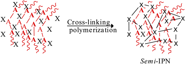
A general methodology for the synthesis of E-semi-IPNs is developed and shown in Fig. 2 via a sequential method. X is a mixture of the cross-linkable monomers, oligomers, or polymers containing cross-linking agent(s) and initiator or initiators. Cross-linking agents can be two-branched, three-branched, or four-branched cross-linkers that are initiated with energy appropriate to either thermal or photoinitiators. Conductive polymer(s) including HTMs and emissive materials with many different emission colors (e.g., RGB and white) (referred to herein as “A” based polymers) can be dissolved or swollen within the X-solution.
Formation of emissive semi-interpenetrating polymer network (E-semi-IPN) via sequential method.
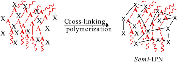
The resulting materials are used to serve as emitting layers in OLED devices. For a proof-of-concept demonstration, the formulated solution with PFO as emissive material undergoes thermally initiated polymerization to give a cross-linked network that provides E-semi-IPNs as expected. This set of materials does not necessarily represent the best formulation, but it suffices for demonstrating the advantages of E-semi-IPNs for OLED applications. PFO-only thin films and devices are used as controls for evaluating blue-emitting E-semi-IPNs.
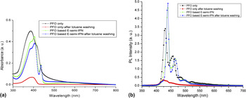
The solvent resistance of thin films of PFO-only and PFO-based E-semi-IPN on DB-coated ITO glass was tested by washing these thin films using common organic nonpolar solvents, such as toluene, dichlorobenzene, p-xylene, that dissolve PFO and also serve for spinning–casting. The representative results using toluene as an example are shown in Fig. 3 through UV–vis absorption and PL spectroscopy. After toluene washing, the UV–vis absorbance of the E-semi-IPN film retains over 85% of its original value, whereas the UV–vis absorbance of the PFO-only film decreases by over 95% [Fig. 3(a)]. Even more importantly, the PL intensity of the E-semi-IPN film remains the same as before toluene washing, compared with negligible emission from the toluene-washed PFO-only film. The nearly 15% loss of UV–vis absorption from PFO-based E-semi-IPN film after toluene washing may be attributed to the removal of PFO that was on the surface of interpenetrating polymer networks but not interlaced with those highly cross-linked polymer networks. Moreover, E-semi-IPN films show a higher PL intensity than PFO-only films even though the PFO absorbance (both peak and integral) of E-semi-IPN films is lower than PFO-only films [Fig. 3(b)]. This indicates that E-semi-IPNs have better internal emission efficiency, which is one of their important advantages over polymer-only emitters when used in OLEDs. Compared with PFO-only films, PFO-based E-semi-IPN films appear to have red-shifted absorption and emission, which result from the formation of a PFO β-phase component. Increased β-phase content has also been linked to an increase in the ratio of singlet to triplet excitons, a decrease in photobleaching, and improved hole mobility.Reference Peet, Brocker, Xu and Bazan18, Reference Ariu, Sima, Rahn, Hill, Fox, Lidzey, Oda, Cabanillas-Gonzalez and Bradley19
(a) UV–vis spectra; (b) PL spectra of poly(9,9-dioctylfluorenyl-2,7-diyl) (PFO)-only and PFO-based E-semi-IPN films before and after toluene washing.

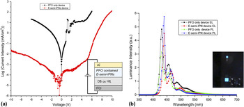
To determine if E-semi-IPNs as emission layers affect EL performance, OLED devices were fabricated with the simple configuration of ITO–glass/DB/PFO-only or PFO-based E-semi-IPN/Al. These simple structures do not represent the optimal situation for a best device performance, but they are sufficient to demonstrate the concept. These sample OLED devices were evaluated by current–voltage (I–V) characteristics and electroluminance (EL) spectroscopy shown in Fig. 4. Compared with the control device using PFO-only as the EML, the PFO-based E-semi-IPN OLED device showed a significantly reduced current leakage, and its luminance efficiency also improved as a factor of two. These results may be attributed to better energy transfer and charge trapping induced by β-phase content in E-semi-IPN films, leading to a better balance of charges and more efficient exciton formation.Reference Lu, Liu, Chang and Chen20 The EL spectrum of PFO-based E-semi-IPN OLED device, similar to the PL study discussed above, also showed a red shift of 10 nm compared with the EL spectrum of the PFO-only device, which further support the existence of PFO β-phase content in E-semi-IPN films and its influence on device performance. As shown in the inset of Fig. 4(b), the OLED device built with a toluene-washed PFO-based E-semi-IPN layer exhibited bright blue emission. This strongly indicates that the inert polymer networks introduced in E-semi-IPN-based OLED devices do not negatively impact device function but help improve the device performance with improved device robustness and solvent resistance. This provides opportunities to incorporate a broader pool of emissive polymers or even possible QD–polymer nanocomposites into the network, optimize the OLED device architecture by multiple layer structures, and build multicolor devices in the fashion of either bottom- or top-emitting device structures.
(a) I–V characteristics of PFO-only and PFO-based E-semi-IPN organic light-emitting diode (OLED) devices; (b) PL and electroluminescence (EL) spectra (Inset: EL images of sample E-semi-IPN OLEDs, which was built with the toluene-washed PFO-based E-semi-IPN layer).

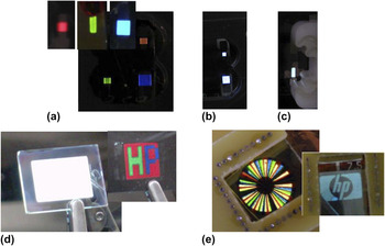
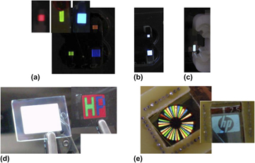
Preliminary results on multicolor E-semi-IPN-based OLED devices are shown in Fig. 5. RGB pixels built on the same chip and different chips [Fig. 5(a)] were achieved with poly[2-methoxy-5-(-ethylhexyloxy)-phenylene-vinylene], poly[9-dioctyl-fluorene-co-benzothiadiazole)], and PFO derivatives based E-semi-IPNs, respectively, deposited either directly on an ITO/DB surface or on top of other E-semi-IPNs layers, RGB on separated chips were also demonstrated, shown at up-left corner of Fig. 5(a). White emission OLED devices in a bottom-emitting structure [Fig. 5(b); glass/ITO/DB/E-semi-IPN/Al, emitting light through ITO glass] and a top-emitting structure [Fig. 5(c); glass/Al/E-semi-IPN/DB/Ag (15 nm), emitting light through semitransparent Ag film] were fabricated with an E-semi-IPN layer with a mixture of RGB polymers in the same polymer networks. Moreover, a white emission OLED panel (1 × 1.5 cm2) with an “HP” logo color filter presents a simpler way to achieve great RGB colors shown in Fig. 5(d); and two demo devices built on PET flexible substrates integrated with segmented backplane on plastic.
(a) Red–green–blue (RGB) pixels on the same chip and different chips prepared from E-semi-IPNs with R, G, B emissive polymer, respectively; (b) bottom-emitting white pixels from an E-semi-IPN with R, G, B emissive polymers; (c) top-emitting white pixels from the same material in (b); (d) bottom-emitting white panel with color filters; (e) demo devices on PET integrated with segmented backplanes on plastic.

B. Hybrid QD–oligomer/polymer nanocomposite
As we discussed above, the inert polymer networks introduced in E-semi-IPN-based OLED devices do not negatively impact device function but help improve the device performance with improved device robustness and solvent resistance. It is noteworthy that a similar scheme could be used to incorporate emissive species like, for example, semiconducting QDs or their mixtures with the appropriate polymer agents to form a multilayer structure since QDs as emitters provide unique properties including narrow emission band, which gives good color purity, great color tenability, and differential stability. In this part of the article, we describe our research findings in developing hybrid QD–OLED pixels where a QD–polymer hybrid nanocomposite is used as the emitter.
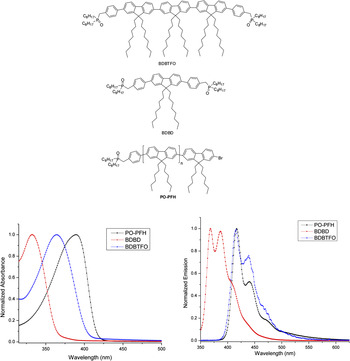
One critical challenge of QD–polymer hybrid nanocomposites is to develop compatible functionalized blue-emitting polymers that can chemically bind or attach to QDs so as to both achieve optimal distribution of emissive inorganic QDs within these polymers and enhance the efficiency of Föster energy transfer from polymers to QDs, thereby getting good device efficiency and improving color purity by quenching the remaining polymer emission. Our first design of these novel materials is to introduce functional groups such as organophosphine oxide into blue-emitting conductive oligomers or polymers to achieve direct attachment of QDs to oligomers or polymer matrix. A number of new organic building blocks have been designed, synthesized, and used either as capping agents or monomers to build novel functionalized oligomers/polymers shown in Fig. 6 via multistep organic syntheses. By reviewing normalized absorbance and emission spectra of our phosphine oxide-functionalized fluorene-based materials, it is seen that oligomer BDBTFO with three fluorene units and two possible binding sites has reasonable chromophore length that shows great photoluminance similarity to polyfluorenes and is also synthesized in a high purity that provides relatively easy control for preparing hybrid nanocomposites. Therefore, this trimer, BDBTFO, was selected as the first candidate to prepare hybrid nanocomposites QD–BDBTFO for a detailed study to prove the concept.
Normalized absorbance (left) and emission (right) spectra of phosphine oxide-functionalized fluorene-based materials.

1. Synthesis of oligofluorene BDBTFO and corresponding hybrid nanocomposite
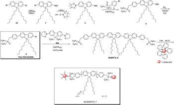
The synthesis of this new material is shown in Scheme 1. The key intermediate to synthesize the target trimer BDBTFO 6 is functionalized fluorene derivative p-2-(7-bromo-9,9-di-n-octylfluorene)benzyl-di-n-octylphosphine oxide (Br-DOF-Bn-DOPO, 5), which was synthesized from 2,7-dibromo-9,9-di-n-octylfluorene via four key steps with an overall yield of about 42%. First, 2,7-dibromo-9,9-di-n-octylfluorene was converted via the monosilyl compound 1 to the boronate 2,Reference Huynh, Dittmer and Alivisatos12 followed by Suzuki coupling of this with p-bromobenzyl di-n-octylphosphine oxide (DOPO-Bn-Br, 3) to give p-(2-(7-trimethylsilyl)-9,9-di-n-octylfluorene)benzyl-di-n-octylphosphine oxide (TMS-DOF-Bn-DOPO, 4) in a very high yield of 93%. The bromodesilylation of TMS-DOF-Bn-DOPO 4 with bromine in the presence of sodium acetate produced the key intermediate 5 in 86% yield without any overbromination. Palladium-mediated Suzuki coupling reaction of key intermediated 5 with 9,9′-dioctylfluorene-2,7-bis(trimethylene borate) in the presence of potassium carbonate afforded bis-functional oligofluorene trimer BDBTFFO 6 with a yield of 50%. Subsequently, oligofluorene BDBTFO reacted with pyridine-capped CdSe/ZnS core–shell QDs in THF via ligand exchange to form hybrid QD–BDBTFO 7 nanocomposite.
Synthesis of oligofluorene BDBTFO and QD–BDBTFO nanocomposite. QD, quantum dot; BDBTFO, Bis-DOPO-Bn-tri-Dioctylfluorene.

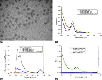
QD–BDBTFO nanocomposite was evaluated by TEM, UV–vis absorbance, and PL measurements. Resulting image and spectra are shown in Fig. 7. TEM image [Fig. 7(a)] shows that CdSe/ZnS core–shell QDs are very well separated without aggregation after BDBTFO ligand exchange process, and distances between QDs are within the range of oligomer BDBTFO’s chemical length. UV–vis, PL, and PLE characterization results indicated that the direct attachment of QDs with conducting oligomers dramatically improves the Föster energy transfer (close to 100%) from oligomer BDBTFO 6 to QDs and give a pure color from quantum-confined CdSe/ZnS nanoparticles. This interesting result provides strong theoretical support to EL devices with improved Föster energy transfer.
(a) Transmission electron microscopy (TEM) image of quantum dot–Bis-DOPO-Bn-tri-Dioctylfluorene (QD–BDBTFO) nanocomposite; (b) UV–vis spectra; (c) PL spectra; (d) photoluminescence excitation spectra of thin films of BDBTFO, QD–BDBTFO, and QD–BDBTFO with additional BDBTFO.

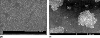
Even though hybrid OLED devices built with this material could not successfully give us convincing EL performance due to poor film formation of QD–BDBTFO nanocomposite, the research findings of QD–BDBTFO nanocomposite are still encouraging, which leads us to a further development on this subject. We have reported a few series of functionalized polyfluorene derivatives, which might have utility to prepare QD–polymer nanocomposite shown in Scheme 2.Reference Guo, Zhao, Pei, Zhou, Gibson, Lam, Brug and Mao17, Reference Guo, Pei, Zhou, Zhao, Gibson, Lam and Brug21, Reference Guo, Liu, Wang, Pei, Zhou, Zhao, Gibson, Brug, Lam and Mao22 As we know amino groups are relatively favored organic functional groups with a good binding property to common QDs such as CdSe/ZnS surfaces, introducing such functionality to conjugated polymer backbone may give us good hybrid nanocomposites. Five amine-functionalized conjugated PFH copolymers (P1–P5) were synthesized with different compositions, which were fully characterized and showed great thermal stability up to 220 °C. The detailed study of their photophysical and electrochemical properties has been reported.Reference Guo, Zhao, Pei, Zhou, Gibson, Lam, Brug and Mao17 From the electrochemical data, it was estimated that band gap of these functionalized polymers was around 2.70 to 3.07 eV for P1–P5, which made them good candidates as host materials for QD–polymer hybrid nanocomposites. However, only P1 showed a good reaction compatibility to form hybrid QD–polymer nanocomposite. Polymer PFH-NH2F-39-1 (P1) was mixed with CdSe/ZnS core–shell QDs with pyridine ligands, in which pyridine ligand was exchanged by the amine functional groups on P1 to form hybrid QD–polymer nanocomposite (QD–P1). Although there was no strong chemical information collected as evidence of polymers directly attaching to QDs, SEM images shown in Fig. 8 revealed that this amine-functionalized copolymer helps QDs well dispersed throughout the thin film, compared with an example of the simple physical mixture of trioctylphosphine oxide-covered CdSe/ZnS in PFO.
Scanning electron microscopy (SEM) images of QD–P1 composites and QD–trioctylphosphine oxide in PFO on Si substrates. Reprinted from Ref. Reference Guo, Zhao, Pei, Zhou, Gibson, Lam, Brug and Mao17 with permission from American Chemical Society.

Design and synthesis of QD–polymer hybrid nanocomposites.

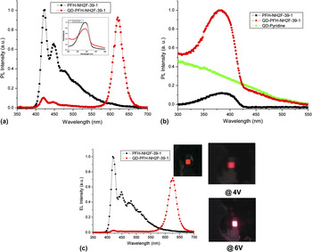
Thin films of QD–P1 nanocomposite were deposited by spin casting from chloroform solutions on quartz substrates for PL and PLE studies. The PL intensity of P1 in this nanocomposite shown in Fig. 9(a) significantly decreases (to <10% of the pure polymer’s emission). Note that the PL emission from the QDs may result not only from the expected energy transfer from the polymer but also from direct excitation. As illustrated in Fig. 9(b), PLE spectrum of the nanocomposite thin film recorded at the maximum of the QD emission (626 nm) exhibits the absorption characteristic features [as shown in Fig. 9(a) inset]. The correspondence between the absorption by the polymer and increased emission by the QDs confirms that when exciting at ∼380 nm, the majority of the QD emission results from energy transfer from blue-emitting polymer P1 to red-emitting QDs. Therefore, a simple proof-of-concept hybrid OLED device was fabricated with the simplest structure configuration of ITO–glass/DB/P1 or QD–P1/Al to learn how effective hybrid nanocomposite works in actual OLED devices. The EL behavior shown in Fig. 9(c) is very similar to their PL behavior, in fact EL spectrum of QD–P1 showed almost none of P1 emitting characteristics. The greatly QD-dominated emission with current efficiency of 0.36 Cd/A from such a simple structure was consistent with efficient energy transfer from P1 to QDs as shown in Fig. 9(c) inset. The QD-only device with the same device structure and fabrication technique was not even operated long enough for EL characterization. The use of hybrid QD–polymer nanocompsite in this simple hybrid OLED device shows a good promise in providing excellent color purity and stability as well as device robustness.
(a) PL spectra of P1 and QD–P1 nanocomposite thin films on quartz substrates (inset shows the absorption of both thin films); (b) PLE spectra of thin films of P1, QD–P1, and pure QDs on quartz substrate. (c) EL spectra of ITO/DB/P1/Al (black square) and ITO/DB/QD–P1/Al (red dot) collected at 6 V (EL spectra of devices were taken in air. Inset: EL picture when the device was operating at 3 V in glove box). DB, DuPont Buffer®. Reprinted from Ref. Reference Guo, Zhao, Pei, Zhou, Gibson, Lam, Brug and Mao17 with permission from American Chemical Society.

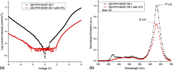
Optimization using more sophisticated device architectures, for example, including HTM semi-IPN as HTL described in the first part of the article and incorporating QD–P1 into semi-IPN to form QD–E-semi-IPNs so as to be able to deposit additional ETL layers, is in progress. Devices with a structure of ITO/DB/HTL/QD–P1/Al are built and gave promising optimization results, where HTM semi-IPNReference Zhou, Sheng, Zhao, Gibson, Lam, Nauka and Brug8 was applied in between DB and QD–P1 (emission layer) as HTL. Figure 10 shows current–voltage (I–V) characteristics and EL spectra of QD–P1-based devices with and without HTL. Compared with QD–P1-only device, the addition of such HTM semi-IPN layer as HTL helped reduce current leakage significantly so as to improve device performance. Through EL spectra [Fig. 10(b)], it can be seen that at 6 V, both devices showed dominated QD emission but with greatly different current density, which is consistent with current leakage improvement. In terms of the spectra, unlike the QD–P1 only device, the HTL/QD–P1 device had no emission peak below 450 nm. Therefore, it may be concluded that HTL is helping not only to balance electrons–holes to reduce the current leakage but also to facilitate energy transfer from polymer to QDs. Overall, the HTL/QD–P1 device showed better efficiency than the QD–P1-only device. More detailed characterization of optimized devices and the relationship of structure tuning and device performance are still needed and will be published in due course.
(a) I–V characteristics of devices ITO/DB/QD–P1/Al (black square) and ITO/DB/HTL/QD–P1/Al (red dot, HTL: HTM semi-IPNs); (b) Normalized EL spectra of these two devices, collected at 6 V (EL spectra of devices were taken in air). HTL, hole transport layer.

IV. CONCLUSIONS
In summary, we have overviewed our general method for developing semi-IPNs that contain an inert, low-cost polymer network and conjugated polymer(s) such as HTMs or emissive polymers. The E-semi-IPNs showed good solvent resistance and retaining of original photophysical properties. In addition, a PFO-based E-semi-IPN OLED device also showed good EL preservation without any negative impact from incorporated inert polymer networks. This may provide an environment for the formation of a β-phase of PFO, which helps improve the charge balance and device performance. We have also showed preliminary results of achieving E-semi-IPN-based multicolor devices with different device structures by a facile solution processing technique without complicated chemical modification or introduction of reactive moieties to OLED material. Hybrid nanocomposite materials have been developed to take advantages from both organic polymer and QDs region. Our research findings from QD–oligomer BDBTFO supported chemical bonding between QDs, and this functional oligomer provides good energy transfer (close to 100%) from oligomer BDBTFO to QDs and give a pure color from quantum-confined CdSe/ZnS nanoparticles. Such a chemical system served as a good analogue directly led to a development of functionalized conducting polymers and their corresponding hybrid QD–polymer composites. Our selected QD–P1 hybrid material showed good promise in providing excellent color purity and stability as well as device robustness. More detailed work on further understanding basics, optimizing materials formulation and device structures, and improving device performance are currently underway.
ACKNOWLEDGMENTS
This work was supported by Hewlett–Packard Company. The authors thank the colleagues of Information Surface Lab at HP Labs for great support and valuable discussions.