I. INTRODUCTION
The results of a predominantly experimental investigation of nanoindentation deformation and cracking of gallium arsenide (GaAs) single crystals are reported in two parent papers. In the first parent paper (part I),Reference Wasmer, Pouvreau, Breguet, Michler, Schulz and Giovanola1 we address the morphology and the kinetics of crack field formation for conical and wedge indenters using in situ instrumented nanoindentation and cross-sectioning techniques by cleavage. We find that the wedge geometry promotes the formation of well-defined half-penny cracks and we establish the kinetics of such cracks with the loading sequence. The observation of slip bands in the indented area suggests that deformation and cracking mechanisms are strongly related. In this paper (part II), we focus on the relationship between deformation mechanisms and crack nucleation.
The industrial production of GaAs laser diodes provides the framework for this study. During the industrial manufacturing process, the separation of laser devices is a critical step, since the active faces of the laser devices have to be atomically flat to guarantee optimal performances. Wafer dicing requires the formation of a precursor crack, obtained either by scratchingReference Wasmer, Ballif, Gassilloud, Pouvreau, Rabe, Michler, Breguet, Solletti, Karimi and Schulz2–Reference Wasmer, Ballif, Pouvreau, Schulz and Michler4 or by nanoindentation,Reference Wasmer, Pouvreau, Breguet, Michler, Schulz and Giovanola1,Reference Pouvreau, Wasmer, Giovanola, Breguet, Michler, Karimi and Gdoutos5 which is then propagated along preferential cleavage planes to separate devices. At present, scratching prevails since the process conditions and the geometry of diamond tools are well optimized to produce suitable precursor cracks. Therefore, deformation and cracking of GaAs during scratching have been well investigated.Reference Wasmer, Parlinska-Wojtan, Gassilloud, Pouvreau, Tharian and Michler6–Reference Wasmer, Parlinska-Wojtan, Graça and Michler8 In the case of nanoindentation, however, the process of forming a precursor crack differs in several ways from that during scratching and results in shorter cracks. It is therefore necessary to have a fundamental understanding of the crack formation mechanisms to optimize the process.
The deformation and cracking of GaAs under indentation/nanoindentation have been studied extensively.Reference Wasmer, Parlinska-Wojtan, Gassilloud, Pouvreau, Tharian and Michler6,Reference Parlinska-Wojtan, Wasmer, Tharian and Michler7,Reference Warren, Pirouz and Roberts9–Reference Largeau and Patriarche21 The dopant type, the doping level, and the indentation temperature are known to have a non-negligible influence on dislocation structures and might explain some of the differences in observations reported in the literature. Nonetheless, the crystallographic orientation seems to play a dominant role in the deformation process and, more interestingly, also seems to influence the cracking patterns around the imprint, as reported by several authors, when indenting (001) planes with a Vickers indenter.Reference Warren, Pirouz and Roberts9,Reference Lefebvre, Androussi and Vanderschaeve19–Reference Largeau and Patriarche21 Warren et al.Reference Warren, Pirouz and Roberts9 observed that cracks were present along the β-dislocation arm ([ $\overline {\rm{1}}$10] direction) and not in the α-arm ([110] direction) and correlated this behavior with the length of β (shorter) and α (longer) arms. They suggested that the different motilities of α- and β-dislocations are responsible for the rosette arm asymmetry and also proposed that dislocation mobility is a major factor in the cracking mechanisms. This correlation was confirmed by indentation experiments conducted by Fujita et al.Reference Fujita, Maeda and Hyodo11 and Maeda et al.Reference Maeda, Nishioka, Narita and Fujita22 on {111} planes at different temperatures. They monitored the brittle to ductile transition by measuring the crack lengths induced by Vickers indentations. By varying both temperature and loading rate, they showed that the cracking behavior of GaAs is controlled by dislocation mobility and governed by an Arrhenius kinetics relation. Several authors,Reference Wasmer, Ballif, Gassilloud, Pouvreau, Rabe, Michler, Breguet, Solletti, Karimi and Schulz2,Reference Bradby, Williams and Wong-Leung15,Reference Le Bourhis and Patriarche17,Reference Giuliani, LLoyd, Vandeperre, Clegg, McVitie and McCombe23,Reference Bradby, Williams and Swain24 indenting GaAs with different indenter geometries, reported that cracks form at the intersection of converging slip bands. Most of the experiments mentioned above were carried out with either Vickers or spherical indenters. In our opinion, studies with this choice of indenters have two main limitations:
(i) they do not investigate the influence of the indenter apex angle;
(ii) the three-dimensional shape of the indenter makes identifying the relationship between the indenter geometry and the dislocation microstructures more complex.
The purpose of the present paper is to investigate differences in the deformation mechanisms as a function of indenter apex angle and to evaluate the influence of these differences on crack nucleation. The wedge geometry was chosen because of (i) the approximate state of plane strain present in the middle of the indenter, which simplifies the characterization and interpretation of dislocation microstructures and (ii) the relevance of the geometry for our study of laser dicing.
Section II of this paper describes the experimental techniques used for the investigation. Section III reports on the results and observations made for wedge indenters with 60, 90, and 120° apex angle. These results are discussed and interpreted in Sec. IV with the help of cathodoluminescence (CL) and transmission electron microscopy (TEM) observations. Finally, Sec. V summarizes the main findings and conclusions of this work.
II. MATERIAL TESTED AND EXPERIMENTAL PROCEDURES
In this work, we investigated commercially available GaAs wafers with a thickness of 350 μm. All wafers were Si-doped (doping level: 1 to 2 × 10⁻¹⁸ cm−3 Si atoms) and electrochemically polished on the (001) plane. Experiments were performed using wedge indenters with 60, 90, and 120° apex angles (see details in part IReference Wasmer, Pouvreau, Breguet, Michler, Schulz and Giovanola1).
We used two different techniques to gather information about the microstructure in the zones under the wedge nanoindenter: CL imaging and TEM. In the case of CL imaging, nanoindentations were performed with a MTS Nanoindenter XP (MTS Instruments, Oak Ridge, TN) with maximum loads in the range of 50–400 mN and at a loading rate of 5 mN/s. Indented samples were prepared using the transverse cross-sectioning technique described in the parent paper (part IReference Wasmer, Pouvreau, Breguet, Michler, Schulz and Giovanola1). They were observed in a Cambridge S-360 Electron Microscope (Leica Cambridge, Cambridge, UK) equipped with an Oxford CL detector and a monochromator.
For TEM observations of transverse cross-sections, the nanoindentation experiments were also conducted on the MTS Nanoindenter XP with a maximum load of 200 mN and at a loading rate of 5 mN/s. We also attempted to characterize deformation at constant penetration depth for wedge indenters with different apex angles. However, the threshold for plastic deformation and cracking is very different for indenters with 60 and 120° wedges, so that the common range of penetration for having sufficient plastic deformation without cracking for both indenter geometries was very small. As a consequence, we could not perform any comparative TEM investigation for the two types of indenters under conditions of equal depth of penetration.
In all cases, the indentation loads were chosen to avoid large extension of the half-penny crack with the 60° wedge indenter.
A first sample of around 1 × 1 cm2 was taken from the wafer. Four sets of nanoindentations were performed on the (001) plane of the sample with:
(i) the 60° wedge indenter with its main edge aligned with the [110] direction of the wafer;
(ii) the 120° wedge indenter with its main edge aligned with the [110] direction;
(iii) the 90° wedge indenter with its main edge aligned with the [110] direction;
(iv) the 60° wedge indenter with its main edge aligned with the [1
 $\overline {\rm{1}}$0] direction.

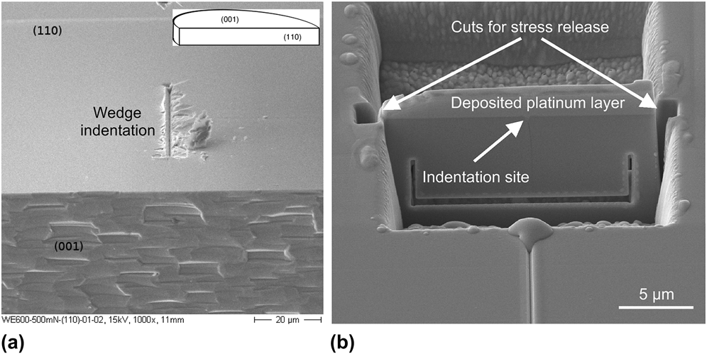
Additional nanoindentation experiments were performed with the 90° wedge indenter on a (110) plane of a second wafer. To obtain a (110) plane, this sample was cleaved using the scribe and break method to obtain a nearly atomically flat (110) surface for indentation. Figure 1(a) shows a nanoindentation performed in the SEM with the 90° wedge indenter at 500 mN. The inset indicates the position of the (110) and (001) planes in the complete GaAs wafer.
(a) In situ SEM nanoindentation performed on a (110) plane with the 90° wedge indenter at 500 mN and (b) preparation of a TEM lamella by FIB milling.

TEM lamellae were prepared by focused ion beam (FIB) milling of the indents using a FEI Strata DB235 FIB (FEI, Hillsboro, OR), as shown in Fig. 1(b). The areas of interest were first covered with a ≈1 μm platinum layer to avoid ion implantation. Then, the lamellae were obtained by ion milling and deposited on a copper grid for TEM observations. Micrographs were obtained with a Philips CM300 TEM (Philips, Eindhoven, Netherlands) operated at an accelerating voltage of 300 kV.
III. RESULTS
A. CL experiments
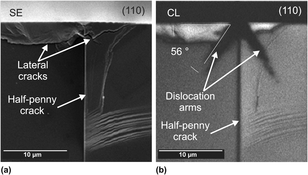
Figure 2 presents two micrographs of the same cross-section of a nanoindentation performed with the 60° wedge indenter. The first image [Fig. 2(a)] was taken in the secondary electron (SE) mode, whereas the second image [Fig. 2(b)] was taken in the CL mode.
SEM micrographs showing the cross-section of a 60° wedge nanoindentation taken with (a) SE and (b) CL.
The SE mode allows us to clearly identify the different crack systems that develop around the nanoindentation, whereas the CL mode provides additional information about the dislocation structure. In the SE image in Fig. 2(a), we clearly identify lateral and half-penny cracks. We note that lateral cracks have reached the surface to form chips. In contrast, the CL images in Fig. 2(b) show an additional feature due to dislocations accumulated in {111} slip planes, while also exhibiting lateral and half-penny cracks. The presence of dislocations is supported by the fact that the angle between the dark contrast band and the surface is approximately 56° which corresponds to the angle between {111} slip planes and the (001) surface plane (54.74°).
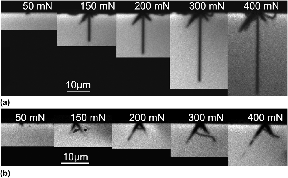
Figure 3 compares the crack and dislocation fields resulting from indentation loads ranging from 50 to 400 mN, for both 60 and 120° wedge indenters on a (001) plane. In Fig. 3(a), for nanoindentations with the 60° wedge indenter, the dislocation arms extend in diverging {111} planes and grow progressively as the load increases, even after nucleation of the half-penny crack. The half-penny crack nucleates at a load of 150 mN and then grows deeper as the load rises. Lateral cracks become visible when the load reaches 300 mN (right side of the nanoindentation). Figure 3(b) shows cross-sections of nanoindentations with a 120° wedge indenter. In contrast to the case of the 60° wedge, and although the figure exhibits a seemingly diverging pattern, dislocation arms extend in converging {111} planes. The convergent structure, revealed by TEM analysis, will be shown in Sec. III. B. No half-penny crack is visible, whereas lateral cracks (visible in SE mode) intersect the {111} planes. Our CL observations confirm the strong interaction between the angle of the wedge, the deformation pattern and the cracking process.
Dislocation and crack fields under (a) 60° and (b) 120° wedge nanoindentations revealed by CL imaging.
B. TEM experiments
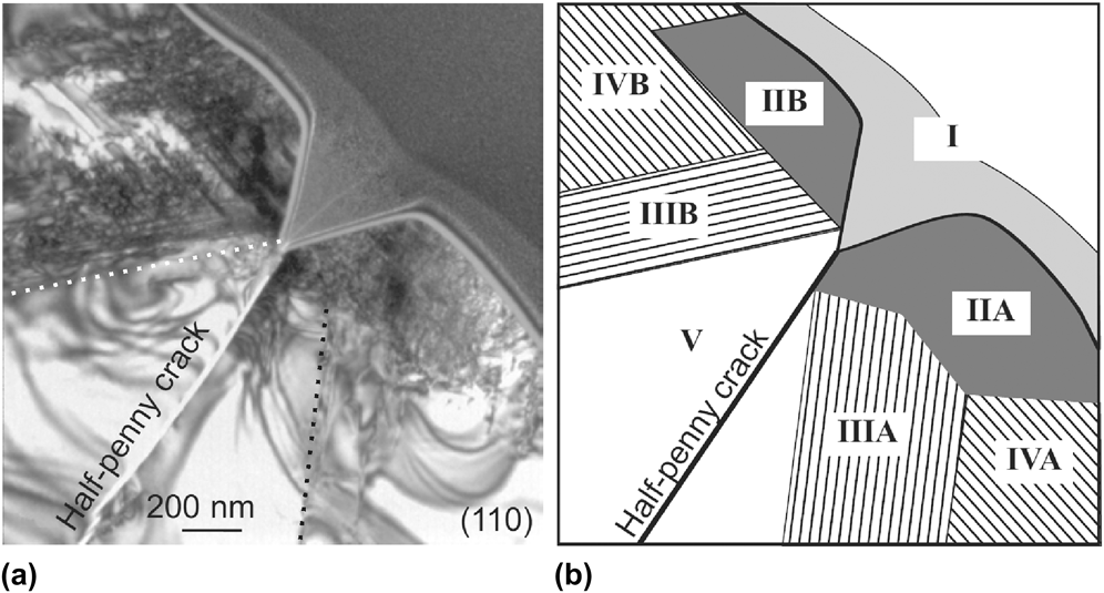
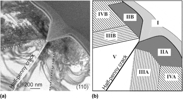
Figure 4 shows a bright-field image and a schematic view of the area beneath an indentation made at 200 mN with the 60° wedge indenter with its elongated edge along the [110] direction. The deposited platinum layer is labeled I on the schematic view. A highly deformed zone extends on both sides of the nanoindentation (areas IIA and B) but not deeper than the residual imprint. The lateral extension of this zone corresponds to the dimension of the pile-up measured at the surface. This zone undergoes the highest deformation and contains a large amount of disordered dislocations. In this area, diverging, converging, and also horizontal portions of dislocations are observed, but no characteristic pattern really emerges. In zone III (A and B), dislocations arrange in a diverging pattern (i.e., the “virtual source” of dislocations is above the indentation surface) following ( $\overline {\rm{1}}$11) (area IIIB) and (1
 $\overline {\rm{1}}$1) (area IIIA) slip planes. These diverging dislocations extend a few micrometers under the indentation area. Area IV is located on both sides of areas II and contains mainly dislocations parallel to the surface, up to a few microns away from the residual imprint of the indentation. Zone V, located directly beneath the apex of the imprint and bounded by the (
 $\overline {\rm{1}}$11) and (1
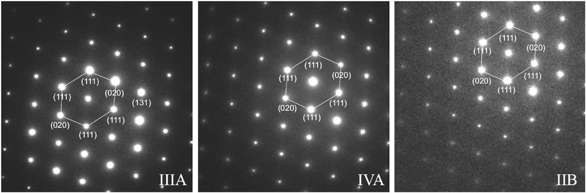
 $\overline {\rm{1}}$1) planes (dashed lines), is free of dislocations. Finally, the 60° wedge indenter is the first indenter geometry allowing a half-penny crack to extend from the apex of the imprint, in a dislocation-free area, rather than from converging slip bands. The crack goes through the entire lamella separating it into two pieces. Note that both parts are only linked together by the deposited platinum layer. Selected area electron diffraction (SAED) patterns taken in the different deformation zones of Fig. 5 (IIIA, IVA, and IIB) exhibit no double spot, an observation indicating that no microtwins are visible.Reference Edington25
(a) TEM micrograph and (b) schematic view of a nanoindentation made with a 200-mN peak load. The main edge of the 60° wedge indenter is along the [110] direction.
Series of SAED patterns taken in different zones under a wedge 60° nanoindentation. The zone axis is [110].
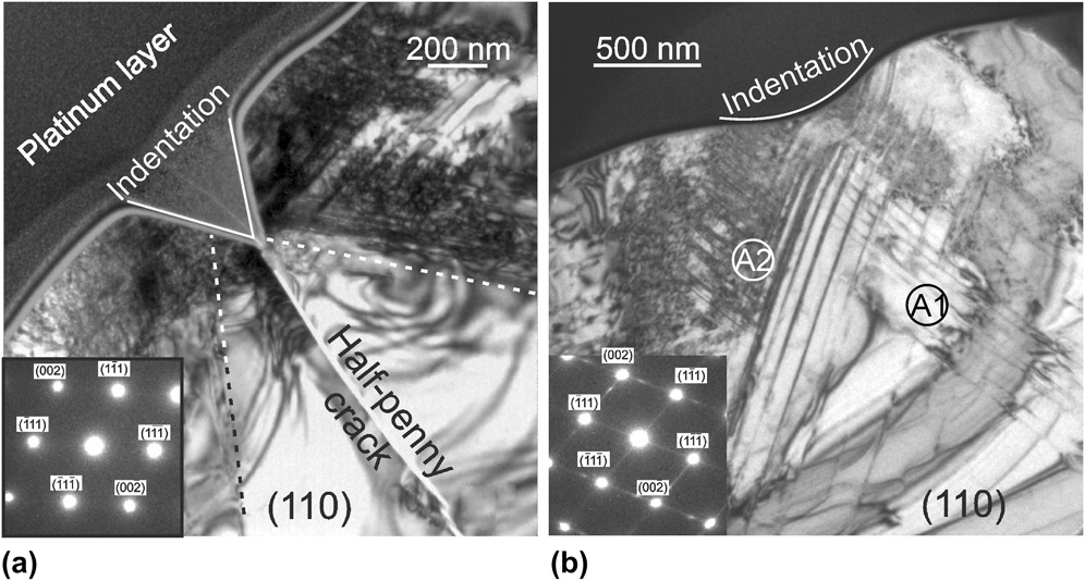
Figure 6 compares the bright-field micrographs of the area beneath two nanoindentations made at a load of 200 mN with the 60 and 120° wedge indenters, respectively. Both indenters have their elongated edge oriented along the [110] direction. The SAED pattern in the inset in Fig. 6(a) is taken under the imprint. As previously observed for the 60° indenter, a highly deformed zone extends under the wedge 120° nanoindentation [Fig. 6(b)], and slip bands in this area are curved. Because the lamella is strongly deformed, convergent beam electron diffraction cannot be performed to estimate the thickness of the lamella and the dislocation density cannot be quantified. Nevertheless, we believe that the curvature of the slip bands is due to interaction forces associated with the high density of dislocations, as demonstrated by Hirth and Lothe.Reference Hirth and Lothe26 In contrast to wedge 60° nanoindentations, the slip bands associated with wedge 120° nanoindentations converge and intersect below the apex of the imprint; no half-penny crack is present. The SAED pattern, taken under the imprint, exhibits double spots and indicates the presence of twinned areas. Figures 7 and 8 present high-resolution TEM (HRTEM) images taken in the areas A1 and A2, respectively. SAED patterns taken in these areas are also shown in these figures. In both figures, the SAED patterns show double spots revealing the presence of microtwins, (in the figures, T stands for twin and M for matrix). The twinning planes are indicated by the dashed lines in the HRTEM. In Fig. 7 (area A1), the twinning planes are (1 $\overline {\rm{1}}$1) planes and the pattern of diffracted beams is rounded due to a slight misalignment of the beam with the [110] zone axis. In contrast, in Fig. 8 (area A2), the SAED pattern reveals two twinning planes, the (1
 $\overline {\rm{1}}$1) and (1
 $\overline {\rm{1}} \,\overline {\rm{1}}$) planes, even though only one twinning plane is visible in the HRTEM image (Fig. 8) taken in the same area.
TEM bright-field micrographs of nanoindentations made with a 200-mN peak load for (a) 60° wedge indenter and (b) 120° wedge indenter. The main edges are along the [110] direction. The insets show the SAED taken under the imprints.
(a) HRTEM micrograph and (b) SAED pattern of area A1 in Fig. 6 (zone axis [110]). The two (1 $\overline {\rm{1}}$1) micro-twinning planes have been highlighted with dashed lines on the HRTEM pictures (T stands for twin and M for matrix).
(a) HRTEM micrograph and (b) SAED pattern of area A2 in Fig. 6 (zone axis [120]). The HRTEM picture shows one of the two existing microtwinning planes [(1 $\overline {\rm{1}}$1) and (1
 $\overline {\rm{1}} \,\overline {\rm{1}}$)]. The microtwinning planes have been highlighted with dashed lines (T stands for twin and M for matrix).
When we indent with the 60° wedge indenter with its main edge aligned with the [1 $\overline {\rm{1}}$0] direction (load 200 mN), as illustrated in Fig. 9, the main deformation and cracking characteristics such as areas of high dislocation density, diverging slip planes, dislocation free area, and half-penny crack are similar to the one observed when the edge is aligned in the [110] direction. However, in this specific case, two main differences emerge. First, the observed slip lines contain either micro-twins or perfect dislocations, as demonstrated in Fig. 9(b). Second, an additional crack (crack 1) runs in a (111) plane propagating from the near apex area of the imprint. Figure 10 is a higher magnification HRTEM micrograph of Fig. 9 showing details of the microtwin labeled T1. For convenience, the (111) twinning planes have been highlighted by dashed lines (T stands for twin and M for matrix).
TEM bright-field micrograph of a wedge 60° nanoindentation at 200 mN made with its main edge aligned with the [1 $\overline {\rm{1}}$0] direction. (a) Overview of the indentation zone and (b) magnified view showing convergent microtwins stopped at the interface with a divergent one.
(a) HRTEM micrograph and (b) SAED pattern of area AI in Fig. 9 (zone axis [1 $\overline {\rm{1}}$0]). The HRTEM picture shows two (111) microtwinning planes that have been highlighted with dashed lines (T stands for twin and M for matrix).
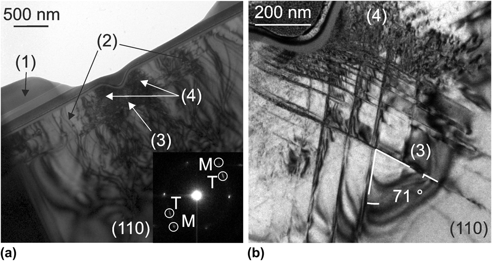
Figure 11 shows a TEM bright-field micrograph of the area beneath a 90° wedge nanoindentation on the (001) plane with its main edge aligned with the [110] direction. The deposited platinum layer (i) has been thinned during the polishing process. Horizontal segments of dislocations (ii) are observed 1–2 μm from the indentation site. An array of converging dislocations (iii) is present just below the imprint. As was the case for wedge 60 and 120° indentations, a zone of high dislocation density (iv) is found on each side of the imprint. The bright-field micrograph in Fig. 11(b) presents a magnified view of the area just below the imprint. The angle between slip planes is about 71°, which confirms the {111} orientation of these slip planes. A few double spots are visible on the corresponding diffraction patterns [see inset in Fig. 11(a)], which demonstrate the presence of microtwins.Reference Edington25
TEM bright field micrograph of a wedge 90° nano-indentation at 200 mN made with the main indenter edge aligned with the [110] direction. The inset is a SAED taken in the left hand side area (T stands for Twin and M for Matrix). (a) area beneath a wedge nanoindentation and (b) presents a magnified view of the area just below the imprint.
Figure 12 shows the dislocation microstructure under the 90° wedge indenter on the (110) plane with the main edge aligned with the [1 $\overline {\rm{1}}$0] direction. It reveals a highly deformed area (A1) located below the nanoindentation and bounded by the dotted line. Both diverging and converging slip planes are activated. The diverging slip bands (red lines) extend from the walls of the imprint, whereas the converging ones (black lines) extend from the free surface on both sides of the imprint. The angle measured between the slip bands and the surface is approximately 109° which corresponds to the angle between {111} slip planes for (011) indented plane (109.47°). A vertical line (noted A2 in Fig. 12) extends below the apex of the imprint. This line could represent the early stage of formation of the half-penny crack. Finally, Table I summarizes the TEM observations presented in this section for various test conditions carried out at a peak load of 200 mN and a loading rate of 5 mN/s.
(a) TEM bright-field micrograph of a wedge 90° nanoindentation at 200 mN on a (110) plane with the main indenter edge aligned with the [1 $\overline {\rm{1}}$0] direction and (b) schematic view of (a) TEM bright-field.
Summary of the results obtained from TEM observations. For each case, the maximum load used is 200 mN and the loading rate is 5 mN/s.
IV. DISCUSSION
In the first part of the discussion, we focus on the effect of apex angle of the indenter on dislocation structure and crack initiation. We then address the deformation process in terms of microtwinning.
A. Effect of wedge apex angle on dislocation structure and crack initiation
The first key observation of our investigation of wedge nanoindentation is the strong interaction between the apex angle of the indenter and the crystallographic structure of GaAs. The different results detailed in the previous sections indicate that dislocations nucleate from the surface of the wafer on both sides of the nanoindentations and not in the bulk, below the apex of the indenter. This result may be surprising, if we consider a perfect atomically flat surface in conjunction with contact mechanics. In such a configuration, it is known that (i) the maximum shear stress is the parameter responsible for the nucleation of dislocations and (ii) the maximum shear stress is located at a depth of more or less ¾ of the tip radius.Reference Johnson27 These stress considerations thus argue in favor of dislocation nucleation sites underneath the indenter. Nevertheless, the view of having dislocations nucleating at the surface is consistent with the literatureReference Wasmer, Parlinska-Wojtan, Gassilloud, Pouvreau, Tharian and Michler6–Reference Wasmer, Parlinska-Wojtan, Graça and Michler8,Reference Mann and Pethica28,Reference Mann and Pethica29 and is supported by 4 observations:
(i) although the GaAs wafers were of excellent quality, the crystal and surface finish quality was not atomically prefect. This implies that some nanometric-size surface asperities existed and significantly affected the initial contact stiffness and the yield point.Reference Mann and Pethica28 Hence, if we take into account nanometric surface inhomogeneities and small impact phenomena (at a velocity of approximately 150 nm/s obtained from the MTS) during initial contact, we may argue that some dislocation lines can be generated even at loads close to zero. Such dislocations may not be stable after unloading unless they have multiplied or have been pinned in some way.Reference Mann and Pethica29
(ii) Under 60° wedge nanoindentations, no dislocations are visible below the apex of the indenter [see Figs. 4 and 6(a)].
(iii) When the apex angle of the indenter is smaller than the angle between {111} planes (the case for the sharp indenter with a 60° apex angle), dislocations initiated in the immediate vicinity of the indenter faces cannot move through the material/indenter interface and the only {111} planes where dislocation motion is possible are diverging ones as already shown by Parlinska-Wojtan et al.Reference Parlinska-Wojtan, Wasmer, Tharian and Michler7 In our experiments, we show in addition that far from the indentation site, motion of dislocations in converging {111} planes becomes possible for specific conditions; but since the stress at that distant location is significantly lower than in the immediate vicinity of the indenter, only small converging dislocations are visible.
(iv) Conversely, when the apex angle of the indenter is larger than the angle between {111} planes (the case for the obtuse indenter with a 120° apex angle), it is geometrically possible for dislocations to propagate in converging {111} planes without crossing the material/indenter interface.Reference Parlinska-Wojtan, Wasmer, Tharian and Michler7 In this case, only converging slip patterns are found.Reference Wasmer, Ballif, Gassilloud, Pouvreau, Rabe, Michler, Breguet, Solletti, Karimi and Schulz2,Reference Parlinska-Wojtan, Wasmer, Tharian and Michler7,Reference Bradby, Williams and Wong-Leung15,Reference Le Bourhis and Patriarche17,Reference Giuliani, LLoyd, Vandeperre, Clegg, McVitie and McCombe23,Reference Bradby, Williams and Swain24
The wedge 60° indenter used, combined with low load levels, as in our experiments, is the only set of conditions, so far, allowing the nucleation of a half-penny crack in a dislocation free region, where only diverging slip systems are activated. This result implies that the general explanation for the nucleation of the half-penny crack in terms of high stress concentrations caused by dislocation pile-upsReference Wasmer, Ballif, Gassilloud, Pouvreau, Rabe, Michler, Breguet, Solletti, Karimi and Schulz2,Reference Bradby, Williams and Wong-Leung15,Reference Le Bourhis and Patriarche17,Reference Bradby, Williams and Swain24,Reference Edington25 is not valid and that another explanation is required.
Under sharp indenters such as the 60° wedge indenter, the lack of plastic deformation by movement of dislocations in the area just beneath the apex of the indenter must create a zone of intense tensile stress, sufficient to break bonds between atoms and initiate a crack. There is a tendency for the tensile stress values to decrease with increasing apex angle of the wedge indenter. This decrease in stress was confirmed by FE calculations (not presented here), where for a fix penetration depth of 1 μm, the peak loads were 530 mN for the wedge 60° and 860 mN for the wedge 120° while the maximum tensile stress values were 1.24 and 0.93 GPa, respectively. Hence, increasing the apex angle of the wedge indenter requires a much higher load for nucleating the half-penny crack, which is consistent with our experimental results. As already mentioned, this result differs from the observations of several authorsReference Wasmer, Ballif, Gassilloud, Pouvreau, Rabe, Michler, Breguet, Solletti, Karimi and Schulz2,Reference Bradby, Williams and Wong-Leung15,Reference Le Bourhis and Patriarche17,Reference Bradby, Williams and Swain24,Reference Edington25 who stated that crack initiation was caused by high stress concentrations coming from dislocation pile-ups. However, this assertion is based on observations for experiments with conical or three-sided indenter geometries such as Vickers, cube corner, or Berkovich indenters. These indenter geometries produce a complex stress field capable of activating three or more {111} planes simultaneously. This geometrical configuration allows dislocations sliding from different {111} planes and pilling-up at one specific location under the tip. The resulting high stress concentration then leads to crack initiation. In contrast, the wedge geometry investigated in this work induces an approximate state of plane strain in the middle of the indenter so that only two {111} planes can be activated at the same time. Considering the case of nanoindentations on the (001) plane with the main indenter edge aligned with the [110] direction, the only possible sliding planes are (111) and ( $\overline {\rm{1}} \,\overline {\rm{1}}$1). This fundamental difference in stress field between previous studies and the present one could be at the origin of the difference in dislocation nucleation sites and cracking mechanisms.
B. Microtwinning
Wasmer et al.Reference Wasmer, Parlinska-Wojtan, Gassilloud, Pouvreau, Tharian and Michler6 found that twinning is the main deformation process of GaAs during indentation, whereas only slip bands and perfect dislocations are seen after scratching. This behavior was explained by the fact that the low indentation velocity allows twins to nucleate and propagate from surface inhomogeneities, whereas in scratching, plastic deformation occurs first in front of the indenter, and the scratching speed allows only α-perfect dislocations to propagate. In our experiments, the indentation velocity was very similar to that in Wasmer et al. (<150 nm/s), but in contrast to these authors, we observed several deformation mechanisms including dislocation motion, slip, and microtwinning. Therefore, a factor other than deformation speed has to play a role to explain the differences in deformation processes observed during indentation. On the basis of observations of nanoindentations made on the (001) plane with the main edge along the [110] orientation, we find that 90 and 120° wedge indenters favor the formation of microtwins, whereas the 60° wedge indenter favors the formation of perfect dislocations. Furthermore, comparison of the SAED patterns taken under 90 and 120° wedge nanoindentations reveals that double spots are more difficult to observe for the 90° angle than for the 120° angle. This observation suggests that the apex angle of the indenter also influences the number of microtwins that are nucleated. As a result, we conclude that for wedge nanoindentations made with the main edge aligned with the [110] direction, a decrease in apex angle induces a transition in deformation mechanisms from mainly microtwinning for large apex angle (i.e., 120°) to mainly nucleation and propagation of perfect dislocations for small apex angles (i.e., 60°).
The second important result of the present study is both the apex angle of the indenter and the crystallographic orientation affects the deformation process. In the case of Vickers indentations, Levade and VanderschaeveReference Levade and Vanderschaeve30 or Koubaïti et al.Reference Koubaïti, Levade, Vanderschaeve and Couderc31 have observed microtwins in the [110] direction and perfect dislocations in the orthogonal [1 $\overline {\rm{1}}$0] arm. The results of these authors have been chosen among many other results since their studies with Vickers nanoindentations were performed under similar conditions as ours (temperature and semiconductor doping type). The presence of microtwins along the [110] direction in the case of 90 and 120° wedge indenters is consistent with the observations of these authors. However, our results with 60° wedge nanoindenters differ, since we observe microtwins forming in the [1
 $\overline {\rm{1}}$0] direction and not in the orthogonal [110] direction. Based on the previous results and keeping in mind that the apex angle of the 60° wedge indenter is much sharper than the apex angle of the Vickers indenter (136°), the influence of the apex angle of the indenter and the crystallographic orientation on the deformation process becomes evident. Though, the fundamental laws explaining completely the deformation process in terms of the apex angle of the indenter and the crystallographic orientation are still not fully understood.
V. SUMMARY AND CONCLUSIONS
The deformation and crack initiation mechanisms under wedge indenters with different apex angles have been investigated by means of CL imaging and TEM observations of thin cross-sections.
In the case of GaAs single crystal, we demonstrate a strong interaction between the crystallographic structure of the material and the apex angle of the indenter. A sharp wedge indenter with an apex angle smaller than the angle between {111} planes (around 71°) generates a diverging structure of dislocations, a dislocation-free area just beneath the indenter apex and a half-penny crack initiating in this dislocation-free area. On the other hand, obtuse indenters (i.e., indenters with an apex angle greater than the angle between {111} planes) generate a convergent pattern of dislocations. For a given indentation depth, the values of the induced tensile stress increase with decreasing apex angle of the wedge indenter. In addition, for large apex angles, the possibility of accommodating large strains beneath the apex of the indenter by movement of dislocations in converging slip planes delays the initiation of cracks.
The formation of microtwins depends on both the orientation of the indenter with respect to crystallographic planes and the apex angle of the indenter. 90 and 120° wedge indenters favor the formation of microtwins, whereas under 60° wedge indenters, deformation occurs essentially by the nucleation and propagation of perfect dislocations.
The principal motivation of this study was the replacement of scratching tools by indentation tools in dicing GaAs laser diodes. In part I of the paper, we demonstrated that the wedge geometry was the most appropriate one to generate a controlled half-penny crack, while minimizing undesirable lateral cracks. In the present article, we have shown that for dicing of GaAs wafers, the opening angle of the indenter must be smaller than 70° to ensure a diverging dislocation structure and to favor the initiation of a half-penny crack. The present conclusions should be valuable for dicing of other single crystal semiconductors with a similar zincblende structure.
ACKNOWLEDGMENT
The authors would like to thank the Commission for Technology and Innovation of the Swiss Government for funding of this work under Grant No. 6025.2.