Introduction
Many wireless communication systems for various working frequencies and communication protocols have been developed and deployed globally in recent years, and the demand for mobile devices operating under various wireless services has increased exponentially. All of these applications operate at a specific frequency, and each would necessitate the use of a separate antenna. A separate antenna for each application will consume a lot of space on the RF boards, making handheld devices bulky. As a result, modern wireless communication systems are evolving toward multifunctionality [Reference Ullah, Ullah, Ahmad, Khan, Ahmad, Habib, Aibreem, Alsharif and Uthansakul1, Reference Bhartia and Bahl2]. Nowadays, multifunctional antennas are in high demand because conventional antennas fail to meet such a multifunctionality requirement, necessitating advanced designs to meet such functionality demands. The reconfigurable antenna is well-known for its ability to change the polarization, frequency, and pattern of wireless communication systems based on current or future demand [Reference Ghaffar, Li and Awan3, Reference Naqvi and Lim4]. The frequency reconfigurable antennas can operate under a variety of standards. According to user end requirements, their ability to handle the same operation as multiple antennas without increasing overall size makes them an excellent choice for handheld devices, and as a result, much effort has been invested in new designs of reconfigurable antennas.
Using two varactor diodes, [Reference Mahlaoui, Antonino-Daviu, Latif and Ferrando-Bataller5] designed a dual-band frequency reconfigurable patch antenna to cover WLAN bands at 2 GHz and a second band ranging from 5.3 to 5.8 GHz. For WLAN and WiMax applications, a new miniaturized switchable band microstrip patch antenna array with eight PIN-diodes was presented [Reference Pandhare and Abegaonkar6]. A triband slot antenna designed to cover the bands of 2.4, 5, and 3.5 GHz for WLAN and WiMAX applications using two PIN diodes was reported in [Reference Younus and Sayidmarie7], with a gain of less than 5 dBi for all operating frequencies. Reference [Reference Ellusamy and Balasubramanian8] describes a quad-band frequency tunable antenna for 5G sub-6 GHz applications that uses three PIN diodes. Although the gain is only 2.3 dBi, this antenna covers 3.31–6.03 GHz in sensing mode and three bands in communication mode, namely 3.31–4.32, 3.78–4.98, and 4.98–5.96 GHz. Reference [Reference Shanmugam9] proposed a simple and compact penta-band frequency-reconfigurable antenna. The patch antenna presented here employs a single PIN diode connected between two rectangular strips to achieve the five frequency bands of 2.4, 3.3, 5.3, 5.9, and 4 GHz. The antenna, however, is only suitable for WLAN and 5G applications, and the gain varies from 2.6 to 5 dBi depending on the operating band. A reconfigurable hexa-band, low-profile monopole antenna designed to cover Wi-Fi, WiMAX, WLAN, and C-Band communications was reported in [Reference Ullah, Ahmad, Khan, Ali, Tahir and Bashir10], with the antenna working efficiently above 90% of the time and an adequate gain of less than 2 dBi. Using three PIN diodes, [Reference Jenath Sathikbasha and Nagarajan11] presented a novel multi-band frequency reconfigurable antenna with a defected ground structure that operated in 12 dissimilar resonant frequency bands centered at 1.36, 1.8, 3.0, 3.9, 5.0, 6.2, 6.4, 7.4, 7.9, 8.2, 8.4, 8.6 GHz. The proposed antenna, however, is only suitable for Wi-Fi, WLAN, and WIMAX applications.
Although the antennas multiband frequency reconfigurable operations have been achieved using various switching techniques and novel concepts, the majority of the antennas cover only Wi-Fi, WLAN, WiMAX, and 5G applications, and the remaining obtained bands do not have very specific wireless communication applications. Furthermore, the use of switching elements in the design increases the reflection loss and complexity of the design, reducing the antenna's gain and bandwidth. However, advancements in modern wireless communication necessitate high performance antenna radiators in terms of bandwidth and gain, as well as reconfigurable operation. As a result, new research on ultra-wideband high-gain reconfigurable antennas has been conducted. Despite the fact that no work had been done to improve the antenna's gain, [Reference Mayuri and Rani12] reported a compact reconfigurable UWB antenna operating at WiMAX and WLAN bands with significant gain reduction at notch band frequencies. Reference [Reference Yang, Yu, Wu and Shen13] described a novel frequency reconfigurable antenna that operated in two single bands, WiMAX and WLAN, and one dual band, WiMAX/WLAN. The gain was reduced in both single and dual bands in this work, resulting in a decrease in overall antenna performance. Reference [Reference Cleetus and Josemin Bala14] described an ultra-wideband and multiband reconfigurable antenna. The antenna structure employs six switches that allow the antenna to reconfigure across seven different frequency bands, the first of which allows the antenna to operate in the band 3.14–10.6 GHz, and the remaining six configurations are found to cover the various narrow bands. However, none of the operating bands have very specific applications for wireless communication, and gain enhancement has also been overlooked. Finally, [Reference Saraswat and Kumar15] reported on a collaborative work on a reconfigurable UWB antenna, in which an octagonal-shaped patch antenna with switchable inverted L-shaped slotted ground was designed using RF switching element PIN diodes. A circular loop frequency selective surface (FSS) was used to improve the fall in antenna gain. However, gain enhancement using FSS has only been studied for the UWB range and not for all switching states. Based on the literature review, it was discovered that combining work on wideband reconfigurable antennas with gain enhancement for all operating bands has yet to be reported.
In recent years, the demand for a single antenna that can support multiple standards such as GSM900, GSM1800, LTE, GPS, 4G LTE, WLAN, WiMAX, and UWB has skyrocketed. This paper proposes a wideband and multi-band on-demand reconfigurable antenna for modern wireless applications in order to provide an advanced on-demand service to the public. A wideband monopole antenna with a switchable slotted ground structure is proposed for use in a variety of wireless applications. Using RF PIN diodes, the proposed antenna operates in six different states, making it suitable for UWB, GSM, GPS, 4G LTE, WLAN, and WiMAX applications. To achieve the desired frequency band state, seven PIN diodes were placed in a slotted ground structure. A multilayer FSS reflector is designed and implemented to improve the gain of the proposed reconfigurable antenna. The FSSs are installed beneath the antenna to act as a reflector [Reference Kushwaha and Kumar16] and improve gain not only for the wideband frequency range but also for all other operating modes. The proposed antenna is designed and investigated in terms of the antenna's various parameters, including impedance bandwidth characteristics, radiation patterns, antenna gain, and radiation efficiency evaluation, using the CST-EM software package.
Antenna design configuration
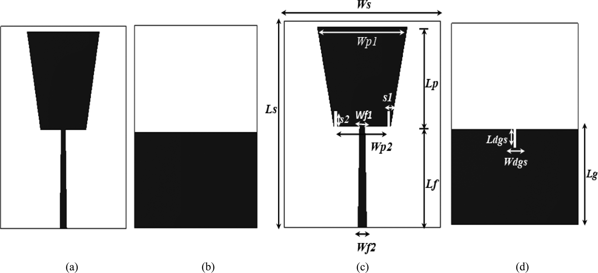
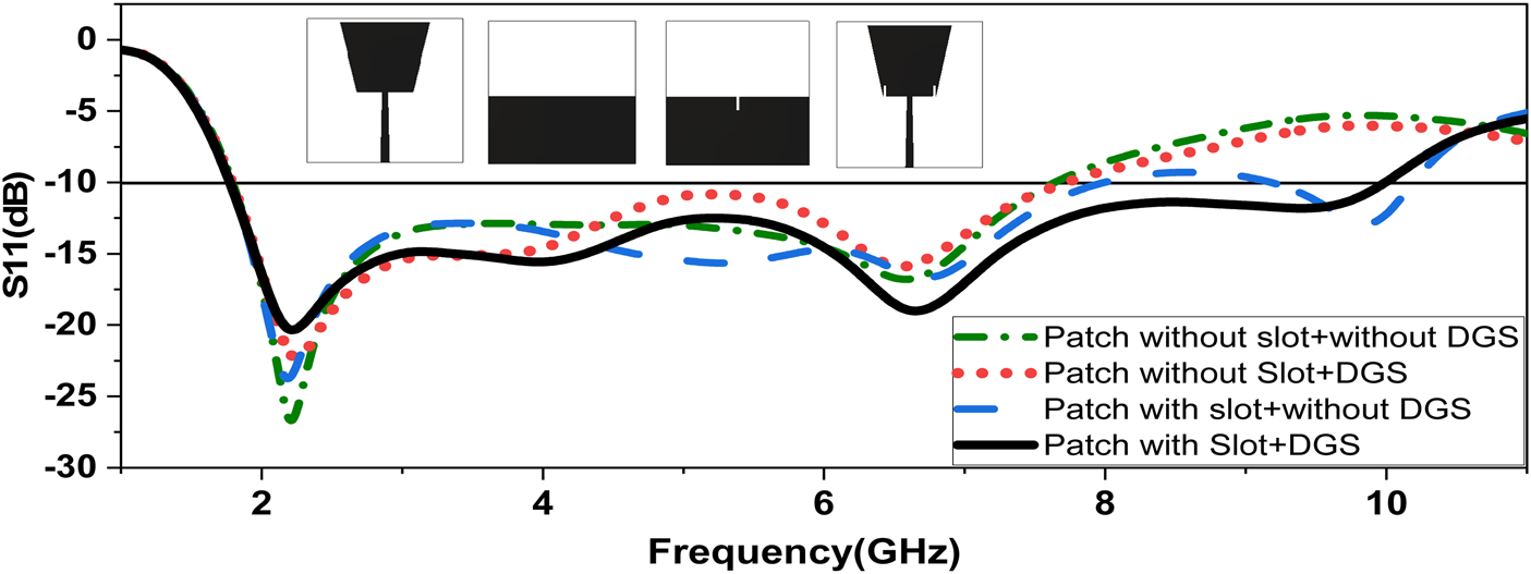
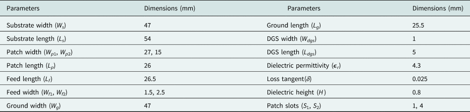
The configuration of the proposed trapezoidal-shaped monopole antenna is shown in Fig. 1. The proposed antenna is fabricated on an FR-4 substrate with a thickness of 1.6 mm, a relative permittivity (εr) of 4.3, and a loss tangent (tanδ) of 0.025. The width (Ws) and length (Ls) of the dielectric substrate material are 47 and 54 mm, respectively. The dimensions of the radiating element patch are Wp 1 = 27 mm, Wp 2 = 17 mm, and Lp = 26 mm. A tapered connection is applied between the feed line and the main radiating patch to improve the antenna performance and achieve 50 ohm impedance matching. The microstrip feed line is a triangular tapered shape with dimensions of Wf 1 = 1.5 mm, Wf 2 = 2.5 mm, and Lf = 26.5 mm. An antenna patch without a slot with a partial ground structure, as shown in Figs 1(a) and 1(b), covers a wide band range from 1.7 to 7.7 GHz. An antenna with two symmetrical slots on a patch without any DGS, as shown in Figs 1(c) and 1(b), covers the 1.7–8 GHz frequency band. Finally, the antenna with symmetrical slots on the patch with DGS, as shown in Figs 1(c) and 1(d), covers an ultra-wideband range from 1.7 to 10 GHz with a percentage bandwidth of 141.8%. In order to improve the wide impedance bandwidth, two symmetrical slots (S 1 × S 2) and a DGS slot (Wdgs × Ldgs) are etched out from the patch and ground plane, respectively. The achieved impedance bandwidth is 141.8% (1.7–10 GHz).
Configuration of the proposed antenna with top and bottom view. (a) Antenna front view. (b) Antenna back view. (c) Antenna front with slotted patch. (d) Antenna back view with defected ground.

Table 1 depicts the optimized design parameters of the proposed antenna and the comparison reflection coefficient plot are shown in Fig. 2.
Simulated return losses of antenna with respect to patch and ground modification.

Design parameters of the proposed antenna

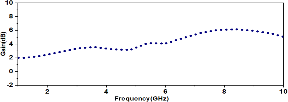
Figure 2 depicts the simulation result of an antenna in terms of patch and ground modification. The proposed antenna has a 141.8% impedance bandwidth (1.7–10 GHz) with a return loss of less than −10 dB and a peak gain of 6 dBi over the entire operating band, as shown in Fig. 3.
Antenna gain versus frequency plot.

Reconfigurable antenna design
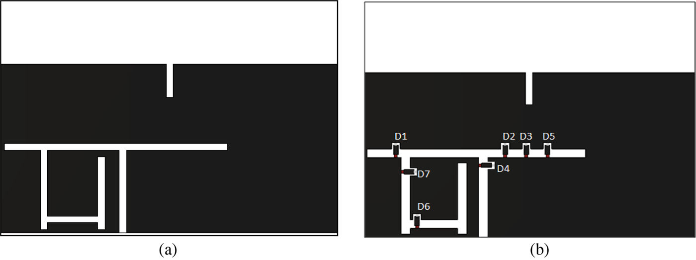
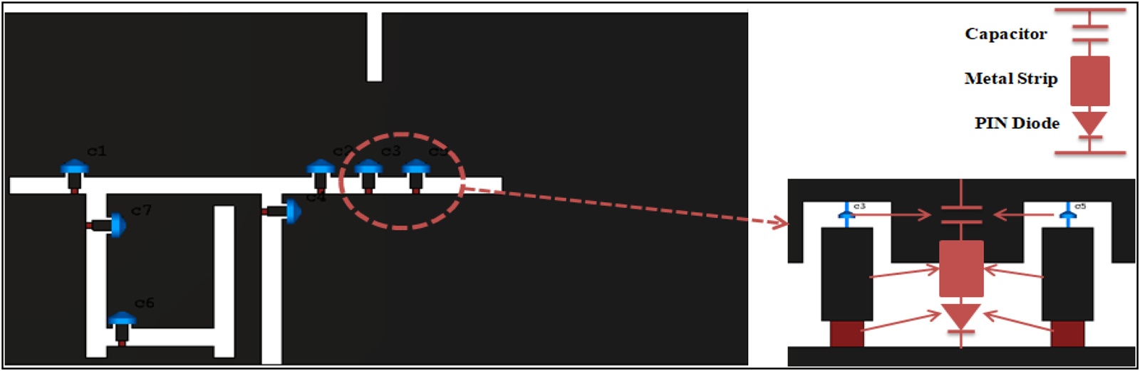
An antenna's basic structure can be reconfigured to achieve other frequency bands by using a slotted structure placed on the ground plane, as shown in Fig. 4(a). A wideband antenna has been reconfigured to the other six different frequency band states by locating the DGS structure at the ground plane. Each slot functions as a filter, producing various resonating bands. The effective length of the slot is optimized to obtain the desired resonating frequency bands. As a result, the positions of seven switches, designated D1–D7, have been optimized to obtain the desired frequency bands by varying the effective length of the slots, as shown in Fig. 4(b). To implement the electronic reconfigurable switching operation in the simulation, an initially ideal PEC strip (0.2 × 0.4 mm2) was used as a switching element, and each PEC strip was replaced by an RF PIN diode in practical conditions. To carry out the tuning operation, a total of seven PIN diodes (PEC strip in ideal condition) labeled D1–D7 were used, as shown in Fig. 4(b). The presence and absence of the PEC strip represent the ON and OFF states of the PIN diode, respectively. As shown in Fig. 5, the capacitor has been connected with each PIN diode (D1–D7) as a lumped element of 1 PF to block the DC and pass the RF signal.
(a) Slotted ground plane. (b) Reconfigurable at ground plane with diodes (D1–D7).

Reconfigurable biasing circuit with DC blocking capacitor at the ground plane.

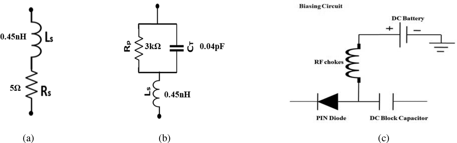
The biasing circuits for each PIN diode are depicted in Fig. 5. Figures 6(a)–(c) show the equivalent circuit of the diode in ON, OFF, and biasing conditions, which includes a PIN diode, a DC block capacitor with RF chokes, and a DC battery.
PIN diode equivalent circuit. (a) ON condition. (b) OFF condition. (c) Biasing circuit.

In the RF (radio frequency) range, the PIN diode functions as a variable resistor for switching purposes. In its OFF and ON states the PIN diode provides an open and short circuit, respectively. In the RLC equivalent circuit, the PIN diode's ON and OFF states represent its forward and reverse bias conditions. In the forward bias, the PIN diode is made up of an inductor (Ls) connected in series with a resistor (Rs), while in the reverse bias, the inductor (Ls) is connected in series with the parallel connection of a capacitor (CT) and a resistor (Rp) [Reference Iqbal, Smida, Mallat, Ghayoula, Elfergani, Rodriguez and Kim17]. In the ON state (forward bias), the equivalent circuit of the PIN diode has a series resistance (Rs) of 5 Ω and a low inductance (Ls) of 0.45 nH. The reverse parallel resistance (Rp) is 3 kΩ in parallel with a total capacitance (CT) of 0.04 pF when the switch is turned off (reverse bias). In the ON state, the forward bias voltage is 0.9 V and the reverse bias voltage is 0 V.
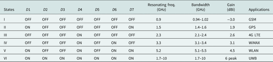
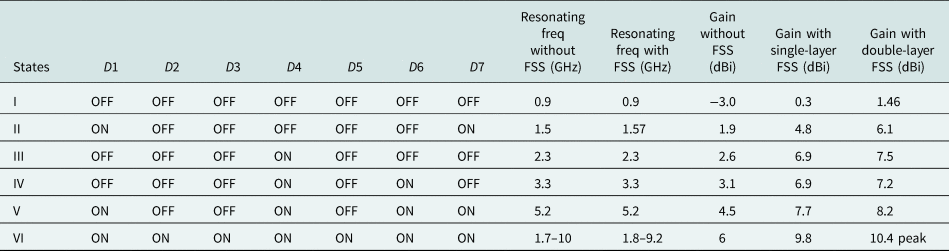
For switching purposes, the MACOM PIN diode model MA4SPS402 was used in the proposed antenna. According to the model's datasheet, it has a lower parasitic inductance of 0.45 nH and an excellent RC constant of 0.23 pS (https://www.macom.com/products/product-detail/MA4SPS402). Table 2 displays the six frequency bands and their corresponding gains and bandwidths in relation to the states of seven PIN diodes.
All frequency bands and corresponding gain with respect to all six states of diodes

The proposed antenna can be reconfigured by electrically controlling the ON and OFF states of the PIN diodes. The following are the operating principles of all six operating states:
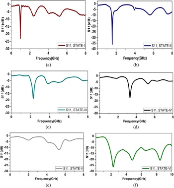
When all of the PIN diodes are turned OFF in state I (no PEC strip during simulation), the length of the resonating structure increases and the antenna resonates in the lower frequency band. For GSM applications, the antenna resonates at 0.9 GHz. However, due to the reduction in gain, an insignificant degradation in antenna performance is observed at this lower frequency. In state II, when PIN diodes D1 and D7 are turned ON (presence of PEC strip during simulation condition) and diodes D2–D6 are turned OFF, the length of the resonating structure decreases as compared to state I, and as a result, the antenna resonates at a trivial higher frequency band. For GPS applications, the antenna resonates at 1.5 GHz. However, as the S-parameter shifts slightly upward, the gain improves. In state III, the PIN diode D4 is turned ON, while the other six diodes are turned OFF, which eventually disconnects the vertical slot with respect to D4 and has a significant impact on antenna performance. As a result, the antenna resonates at a higher frequency band than in states I and II. For 4G LTE applications, the antenna resonates at 2.3 GHz. In addition, as the S-parameter shifts slightly upward in comparison to states I and II, gain improves. In state IV, the PIN diodes D4 and D6 are turned ON, while the other five diodes are turned OFF. This disconnects the vertical slot with respect to D4 and D6, resulting in a significant reduction in the length of the resonating structure. When compared to states I through III, this antenna resonates in a higher frequency band. For WiMAX applications, the antenna resonates at 3.3 GHz. When the PIN diodes D1, D4, D6, and D7 are turned ON and the diodes D2, D3, and D5 are turned OFF in state V, only one horizontal slot up to length D1 is subsequently affected. The single horizontal slot will significantly shorten the length of the resonating structure when compared to the other states, causing the antenna to resonate at a higher frequency band than in states I–IV. For WLAN applications, the antenna resonates at 5.2 GHz. When all of the PIN diodes are turned on, only the trapezoidal-shaped monopole antenna is excited, which has a wide impedance band and a peak gain of 6 dBi as shown in state VI. Figures 7(a)–(f) depict the reflection coefficient (S 11) plot for all six different states (states I–VI) of the proposed antenna.
Reflection coefficient (S 11) plots of all operational states (I–VI), (a) to (f).

FSS design configuration
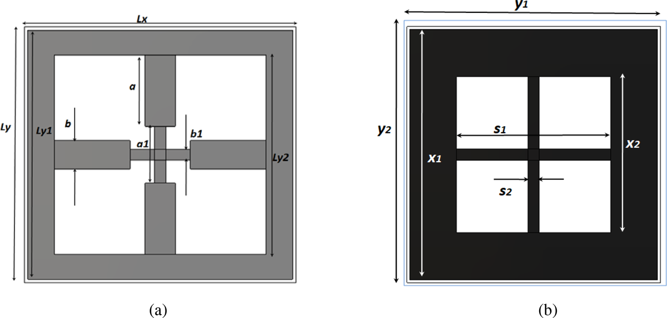
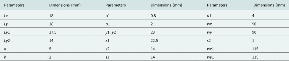
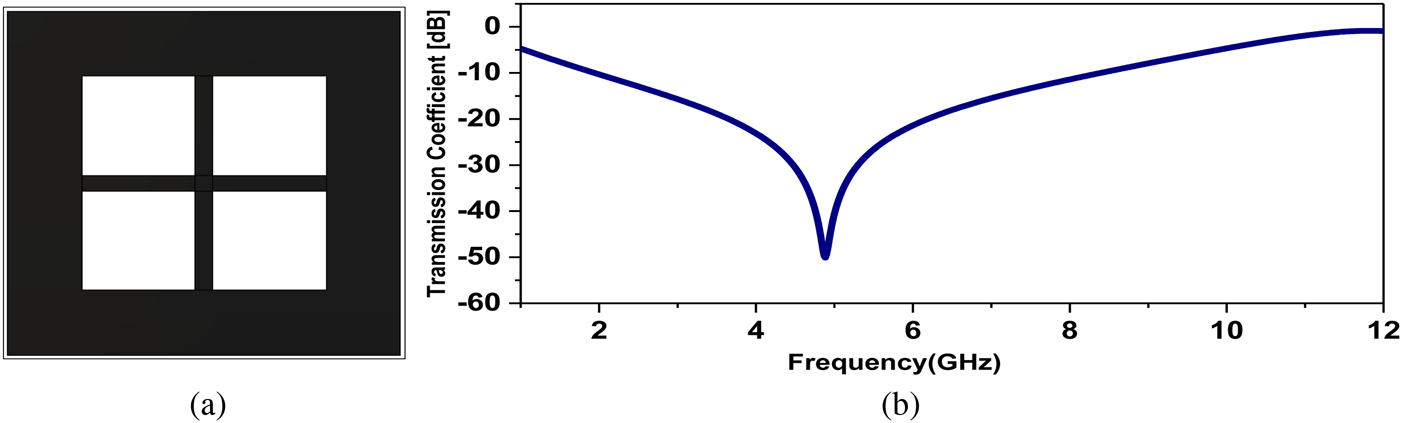
An FSS array has been incorporated as a reflector behind the antenna to improve antenna performance. The unit cell elements of FSS-1 and FSS-2 are depicted in Figs 8(a) and 8(b), respectively. Table 3 depicts all of the FSS-1 and FSS-2 design parameters. The FSS-1 and FSS-2 unit cell elements are designed, simulated, and analyzed using the FEM and the Floquet mode port (finite element method).
(a) Unit cell FSS-1. (b) Unit cell FSS-2.

Parameters of proposed FSS unit cell

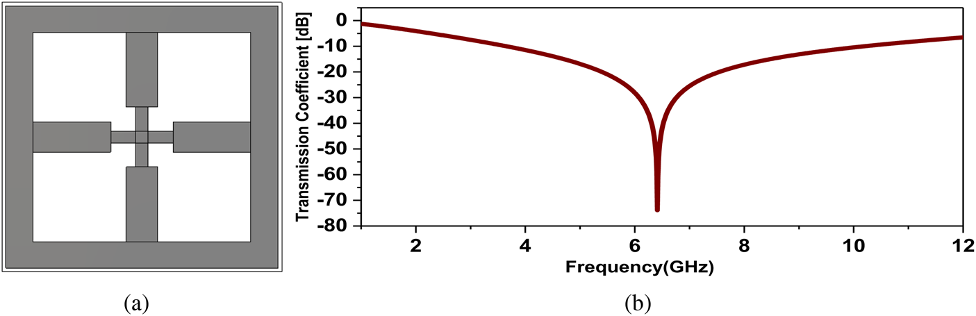
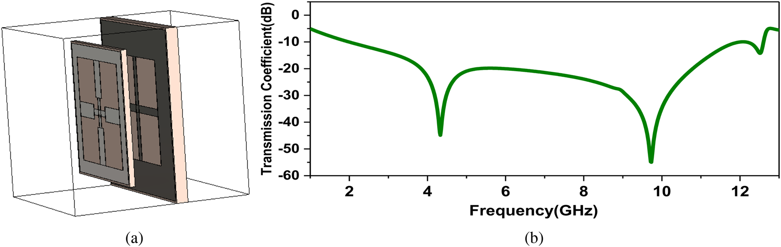
FSS-1 is constructed on the RT 5880 dielectric material having a relative permittivity (εr) of 2.2 and a loss tangent (tanδ) of 0.0009 with an overall size of 18 × 18 × 0.76 mm3. FSS-1 was able to achieve a wide frequency band of 3.6–10.1 GHz. Similarly, FSS-2 is printed on FR-4 dielectric material having a dielectric constant (εr) of 4.3 and a loss tangent of 0.025 with an overall dimension of 23 × 23 × 1.6 mm3. It is designed and optimized in such a way that it achieves a wide frequency band ranging from 1.8 to 8.3 GHz. Further with the aim to achieve a wider bandwidth in UWB range, both the FSS layers (FSS-1 and FSS-2) are cascaded and optimized with a gap of 4.4 mm and obtained the large frequency band range from 1.9 to 12.6 GHz. The unit cell structure and transmission characteristics of the FSS-1, FSS-2, and the cascaded FSS layer are represented in Figs 9–11, respectively.
(a) Unit cell FSS-1. (b) Transmission coefficient of unit cell FSS-1.

(a) Unit cell FSS-2. (b) Transmission coefficient of unit cell FSS-2.

(a) Cascaded form of unit cell FSS-1 and FSS-2. (b) Transmission coefficient of cascaded FSS-1 and FSS-2.

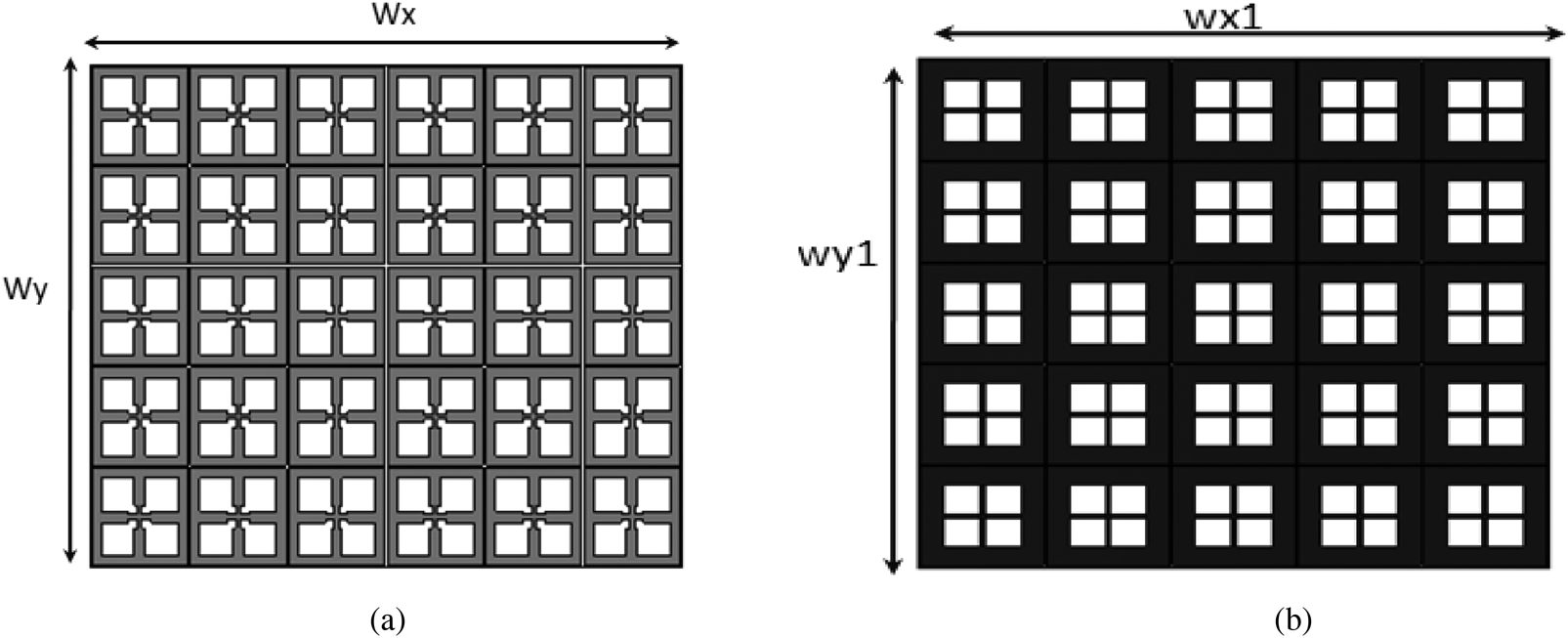
Figures 12(a) and 12(b) show the 6 × 6 and 5 × 5 arrays of the FSS-1 and FSS-2 layers, respectively, and further integrate them with the proposed antenna as a reflector surface. For FSS-1, the vertical and horizontal spacing between two consecutive FSS unit cells g 1 is 0.384λ (here λ is corresponding to the transmission coefficient frequency 6.4 GHz). For FSS-2, the vertical and horizontal spacing between two consecutive FSS unit cells d 1 is 0.377λ (here λ is corresponding to the transmission coefficient frequency 4.9 GHz).
(a) Array of unit cell FSS-1. (b) Array of unit cell FSS-2.

Antenna with FSS superstrate
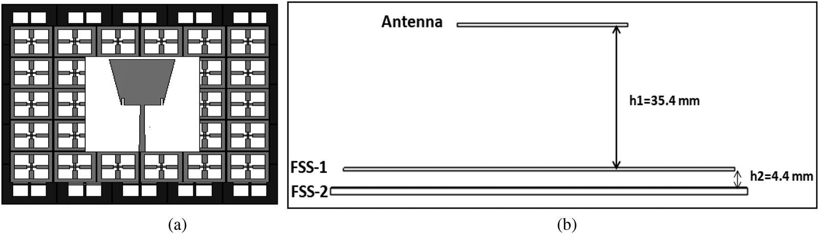
An array of unit cell FSS elements, FSS-1 and FSS-2, is incorporated at the rear of the proposed antenna to achieve the gain increase. Figures 13(a) and 13(b) show the front and side views of an antenna with a double-layer FSS array, respectively. To achieve the gain enhancement, the FSS is placed behind the antenna and optimized so that the transmitted wave from the antenna and the reflected wave from the FSS are in phase. As a result [Reference Kushwaha and Kumar18] represents the state in which the transmitted and reflected waves should be in phase.

(a) Front view of antenna integrated with FSSs. (b) Side view of antenna with double-layer FSSs.

In equation (1), ϕ FSS is the FSS reflection phase, β is the propagation constant (β = 2π/λ), and h 1 is the optimal height between an antenna and FSS.
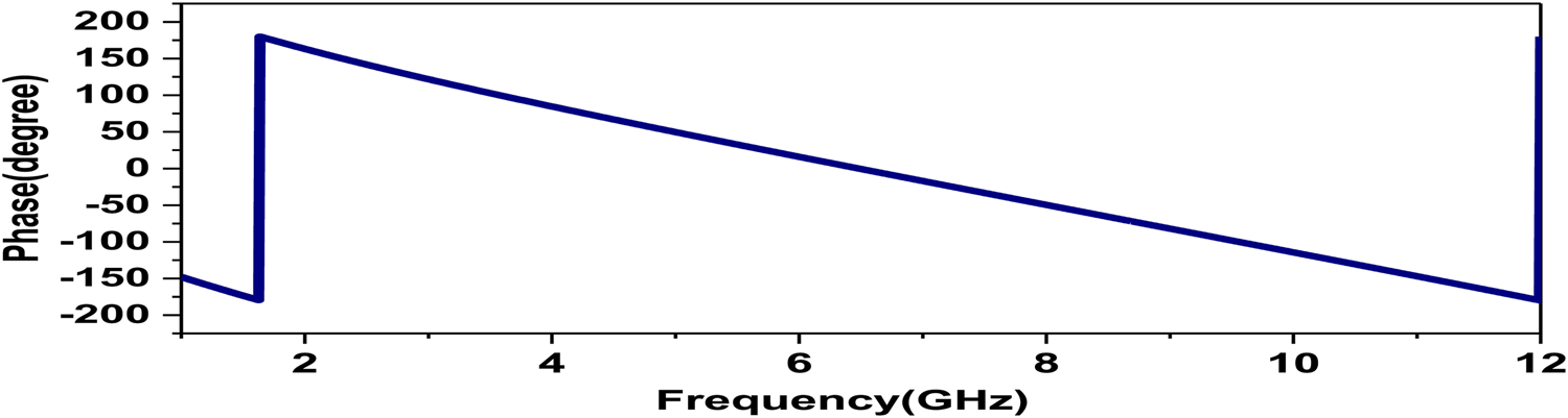
In Fig. 14, the zero degree reflection phase frequency is found to be 6.4 GHz and the optimal height between the FSS and the antenna is calculated to be h 1 = 23.4 mm. However, to achieve the desired bandwidth and reflection coefficient below −10 dB, the height ‘h 1’ needs to be optimized.
Reflection phase of FSS in degree.

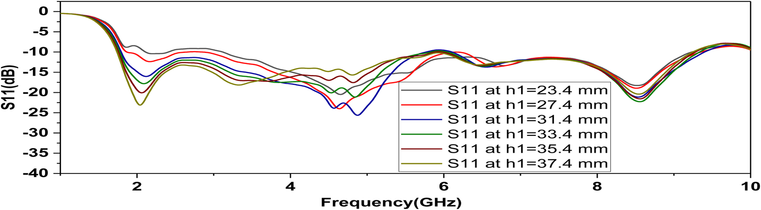
Figure 15 shows the comparison of the simulated reflection coefficient with FSS for the calculated and optimized height at h 1 = 23.4, 27.4, 31.4, 33.4, 35.4, and 37.4 mm.
Parametric analysis of height (h 1) between antenna and FSS for S 11.

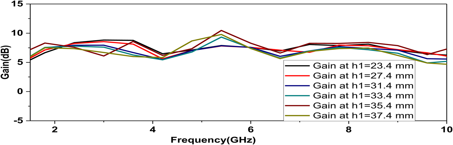
It can be observed that the impedance bandwidth is intact even after the application of FSS. However, to achieve a reflection coefficient of less than −10 dB, the height h 1 must be optimized and found to be 35.4 mm. Similarly, the comparison of the simulated gain of the UWB antenna with FSS at calculated to optimized height at h 1 = 23.4, 27.4, 31.4, 33.4, 35.4, and 37.4 mm has been observed. Figure 16 shows the comparison. It has been observed that when an antenna is placed at an optimized height of h 1 = 35.4 mm with an FSS reflector, then the gain of the antenna is significantly increased by around 3–6 dBi over the complete UWB range.
Parametric analysis of height (h 1) between antenna and FSS for gain.

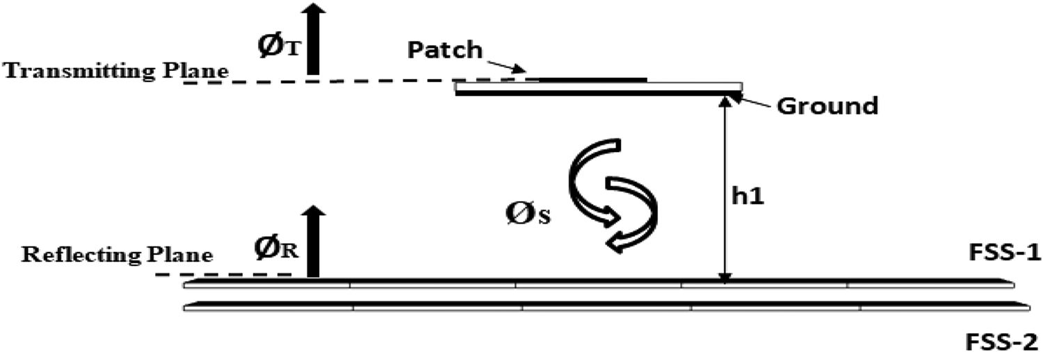
Finally the multilayer FSSs are positioned h 1 = 35.4 mm below the patch antenna. The upper layer functions as a band stop filter, reflecting higher frequency bands while passing lower frequency bands. The lower layer is in charge of reflecting the wave that passes through the upper layer. The working principle of FSS after integration with the antenna is depicted in Fig. 17.
Operation mechanism of multilayer FSS reflector with antenna.

The reflection phases of the upper layer and lower layer are denoted by Ø1 and Ø2 respectively. The overall reflecting phase of multilayer FSS is denoted by ØR. The wave transmitted from the antenna is reflected back by FSS and would combine with the direct wave radiated from the antenna in the opposite direction of FSS. Hence, it results in excellent enhancement of gain after the combining of two components, which gives constructive interference.
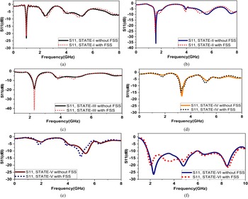
The electromagnetic performance is hampered by the FSS, which is located behind the antenna. Figures 18(a)–(f) compare the simulated reflection coefficient with and without FSS for each of the six states. Even after the application of FSSs, the impedance bandwidth remains intact, but a trivial increase in gain is observed at height (h 1) of 35.4 mm.
(a–f) Comparison of reflection coefficient with and without FSS for all states (I–VI).

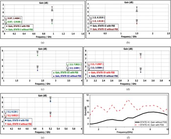
Figures 19(a)–(f) show the antenna gain versus frequency 1D plots for all six states of different frequency bands with and without FSS. It can be seen that the integration of FSS as a reflector behind the antenna results in excellent gain enhancement across all operating bands.
1D plots gain versus frequency with and without FSS for all states (I–VI), (a) to (f).

Table 4 shows the peak gain of the proposed antenna for all single bands and wide bands with and without FSS. It demonstrates gains for all antenna states (I–VI) after FSS application. On the other hand, all of the antenna's frequency bands, with and without FSS, are very similar, and there is no difference. The proposed antenna with FSS exhibits excellent gain enhancement across all operating frequency bands, including wideband.
Comparison of S 11 and gain of all frequency bands with and without FSS

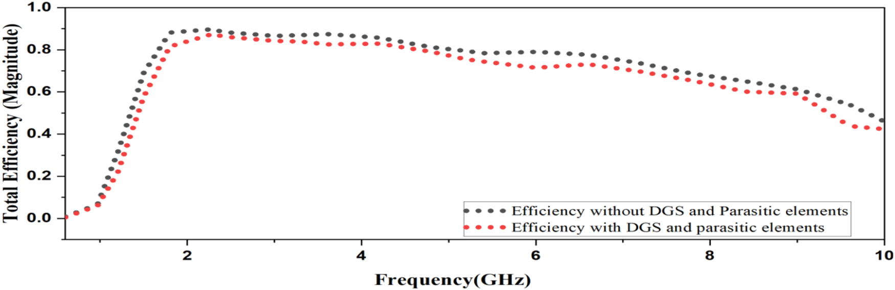
Figure 20 depicts the total efficiency of the proposed antenna with and without DGS and parasitic elements. According to the graph, the efficiency of the proposed UWB antenna alone, when compared to DGS and parasitic elements, was reduced with the integration of DGS and parasitic elements. However, the reduction is only 2–8%, making the proposed antenna suitable for a variety of wireless applications even after the addition of DGS and parasitic elements.
Simulated total efficiency of antenna with and without DGS with parasitic elements.

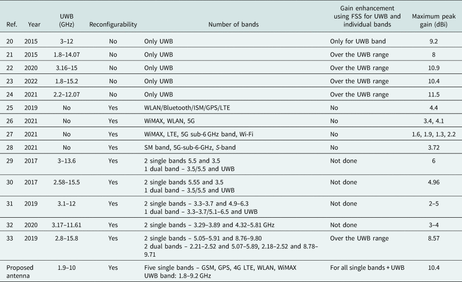
Table 5 compares the proposed work to previously published work in the open literature. References [Reference Yahya, Nakamura and Itami19–Reference Al-Gburi and Ibrahim23] show only UWB antennas that use FSS for gain enhancement, whereas references [Reference Dharani, Rajesh, Madhav and PrudhviNadh24–Reference Ghaffar, Li, Awan, Iffat Naqvi, Hussain, Falcone and Limiti27] show only reconfigurable operation of a low gain antenna that does not even operate in the UWB range. Reconfigurability for UWB antennas is represented by references [Reference Kakhki and Rezaei28–Reference Saraswat, Kumar and Kheir31]. However, no work has been done to improve an antenna's gain. Gain enhancement has been demonstrated in reference [Reference Mayuri and Rani12] only for the UWB range and not for other reconfigured frequency bands. As shown in Table 4, reconfigurability is used in the proposed work to achieve five single bands and one wide frequency band, and an FSS reflector is used to increase the gain of all frequency bands. According to a review of previous published work available in the open literature, no such work has yet been reported in which gain enhancement has been done not only for the wideband antenna but also for all reconfigurable bands using an FSS structure or any other gain enhancement technique.
Comparative analysis of the proposed antenna with few published research works

Measurement test setup and results discussion
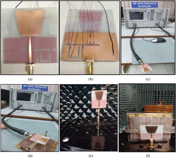
The proposed antenna and FSS structure have been built and tested. The fabricated antenna and measurement test setup for a fabricated prototype antenna assembled with FSS are shown in Fig. 21. The Keysight Vector Network Analyzer (N9918A) is used to test the reflection coefficient (S 11), and the radiation patterns are measured inside an anechoic chamber with an antenna measurement system.
Fabrication and measurement setup of proposed antenna assembled with FSS. (a) and (b) Antenna top and back view. (c) and (d) S 11 measurement of antenna alone and with FSS using VNA. (e) and (f) Radiation pattern measurement inside anechoic chamber.

Reflection coefficient (S 11) characteristics
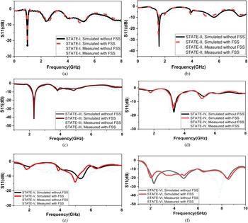
Figure 22 depicts a comparison of the simulated and measured reflection coefficients (S 11) of the proposed antenna with and without FSS for all six switching states (a–f). For all switching configuration states, there is close agreement between the simulated and measured results. The minor variations are due to fabrication tolerances and assembly errors.
(a–f) Comparison of simulated and measured reflection coefficient with and without FSS for all six states (I–VI).

Radiation patterns
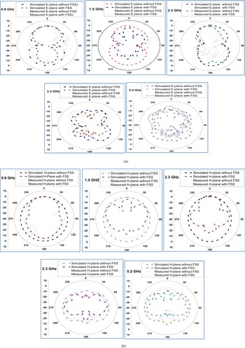
Figure 23 depicts the simulated radiation patterns in the E and H-planes of the proposed wideband antenna with and without FSS at 0.9, 1.5, 2.3, 3.3, and 5.2 GHz. Over the entire ultra-wideband bandwidth, the antenna alone has almost stable radiation patterns with omnidirectional characteristics in the H (X–Z)-plane (φ = 0°) and bidirectional in the E (Y–Z)-plane (φ = 90°). At higher frequencies, the FSS antenna exhibits unwanted side lobes with the main lobe due to higher-order mode excitation and suppresses the back lobes due to the FSS reflector.
Comparison plot of simulated radiation patterns (E-plane and H-plane) of antenna with and without FSS at different frequencies 0.9, 1.5, 2.3, 3.3, and 5.2 GHz. (a) E-plane. (b) H-plane.

Peak gain
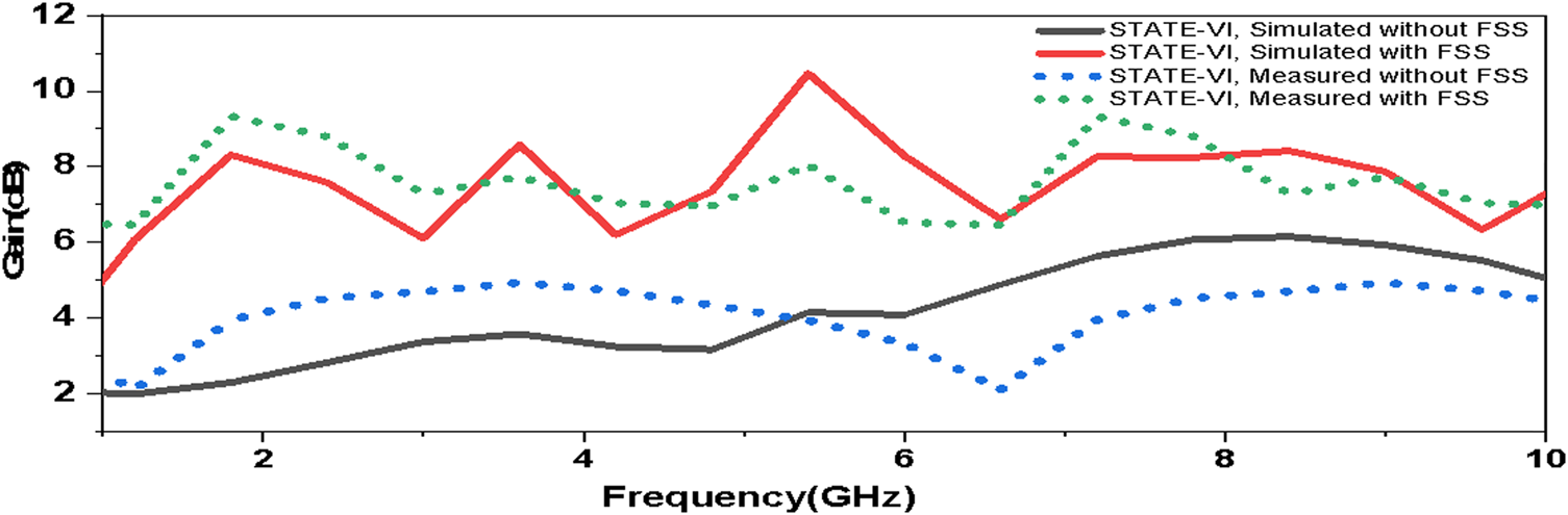
Figure 24 depicts a comparison of simulated and measured gain for state-VI with and without FSS. It can be seen that when an antenna is combined with FSS, its gain improves by about 3–6 dBi when compared to the antenna alone. There is a high degree of agreement between the simulated and measured results.
Comparison of simulated and measured gain with and without FSS.

Conclusion
This paper presents an ultra-wideband reconfigurable antenna with a multilayer FSS reflector to improve the gain across all operating bands. The proposed antenna covers all application bands between 0.9 and 10 GHz. The proposed antenna can be used for GSM, GPS, 4G LTE, WLAN, WiMAX, and UWB applications, providing the public with advanced on-demand service for modern wireless applications. The proposed single UWB antenna can replace five different narrowband antennas while also meeting the requirements of a wideband antenna, resulting in a reduction in the total number of antennas. This work provides more antenna functionality at a lower cost and in a significantly smaller size and space. The proposed antenna with FSS prototype model was constructed, and a good agreement of simulated results with experimental results was observed, making the proposed antenna suitable for integration in portable electronic devices as well as useful for 5G and multiple wireless applications.
Acknowledgements
The authors would like to thank The Science and Engineering Research Board (SERB), Department of Science and Technology, Government of India, for their assistance and support with this work (Grant File No. EMR/2016/007229/EEC).
 Rashmi A. Pandhare completed her Ph.D. in antenna for wireless applications from the University of Nagpur, India in 2018. She has joined Indian Institute of Information and Technology (IIIT) Nagpur in 2019, where she is currently working as an Assistant Professor. She has more than 14 years of teaching experience. She is currently working on one SERB-funded project on ‘High gain reconfigurable antenna for wide band application’ and another DST-funded project on ‘Design and Development of a Mobile App Interface and a Smart Wearable Device for awareness, Tracking and Alerting the Citizens to inculcate Improved Risk Understanding’. She has completed two minor research projects on antenna with DGS for wireless applications. She has published more than 20 papers on antenna for wireless communication in reputed journals. Her research interests include reconfigurable antennas, antennas for biomedical applications, antennas for 5G technology, high gain and UWB antennas, FSS structures and antenna radome.
 Mahesh P. Abegaonkar completed his Ph.D. in microwave sensors from the University of Pune, India in 2002. He worked as a Post-Doctoral Researcher and an Assistant Professor (Contract) in the School of Electrical Engineering and Computer Science, Kyungpook National University, Daegu, South Korea during June 2002–January 2005. In February 2005, he joined the Centre for Applied Research in Electronics (CARE), Indian Institute of Technology (IIT) Delhi where he is currently an Associate Professor. He is a Senior Member of IEEE and Young Associate of Indian National Academy of Engineering (INAE) since 2013. He was Secretary and Treasurer of IEEE MTT-S Delhi Chapter during 2008–2017 and Vice-chairman during 2017–18. He was National Coordinator of Virtual Laboratories under ECE vertical, an initiative of MHRD, Govt. of India under the National Mission on NMEICT. His research interests include microwave and millimeter-wave metamaterial, millimeter-wave antennas for 5G communications, MIMO, printed antennas reconfigurable, broadband, high gain, etc.
 Chandresh Dhote received his B.E. degree in electronics and communication engineering from Radharaman Engineering College (R.E.C.) Bhopal, MP, India in 2014 and the M.E. degree in electronics and telecommunication from Shri. G.S. Institute of Technology and Science (SGSITS), Indore, MP, India in 2017. He has more than 2 years of working experience as an Application (Technical Support) Engineer of CST EM simulation Software. He has given technical support for strategic key accounts to ISRO, DRDO, R&D, key educational institutes and industries. Currently he is working as a JRF (Junior Research Fellow) on high gain reconfigurable antenna for wide band application in IIIT Nagpur since November 2020. His research interests include microstrip antennas, FSS, EBG, filters, waveguide components, radar, and radome. He has published quite a few papers in international conference and journals of repute.