


I. INTRODUCTION
Recently, there has been a steadily growing interest, among the scientists, in developing high-power semiconductor devices for applications in mm-wave systems [Reference Trew1]. The wide band gap semiconductor materials have attracted much attention for possible insertion in military power electronic device applications such as high-power switching devices, high-frequency, high-power amplifiers for electronics communication [Reference Buniatyan and Aroutiounian2]. For realizing higher RF power (P RF) from an IMPATT device, one should choose a semiconductor material that has high value of electric field (E c) and saturated carrier velocity (V s), since the P RF of an IMPATT device is proportional to E c2V s2. Although the conventional IMPATT diodes fabricated on GaAs, InP, and Si are found to be reliable, these are limited by power and operating frequencies due to the fundamental limitations of the material parameters. In addition, the other properties of GaN such as large energy band gap, high carrier saturation velocity, and relatively small dielectric constants make them suitable for high-power, high-frequency oscillators [Reference Shur3, Reference Mishra, Wu, Kellar, Kelar and Baars Den4]. On the other hand, silicon carbide (SiC) is now been accepted as an attractive semiconductor material for realization of high-power, high-temperature, and high-frequency electronic devices because of its favorable properties such as wide band gap, high breakdown field, high thermal conductivity, and high saturation electron drift velocity [Reference Elasser and Chow5]. The high-temperature tolerance for SiC helps in device processing technology [Reference Casady and Johnso6]. The nature provides SiC in more than 100 poly-type structures. The most common poly-types of SiC currently being developed for the realization of electron devices are the cubic 3C-SiC, the hexagonal 4H-SiC, and 6H-SiC crystals. It is also well known that heat generation and dissipation in IMPATT diodes can severely limit the performance of IMPATT diodes. SiC is, therefore, an ideal semiconductor for IMPATT diodes because SiC offers (i) a 10 times higher critical field, (ii) twice the carrier saturation velocity, and (iii) three times the thermal conductivity, in comparison with the low band gap materials such as Si and GaAs. These properties can lead to good-performance IMPATT diodes for microwave and millimeter-wave applications [Reference Neudeck7]. Further, the RF power produced and the efficiency realized in these cases fall to sufficiently small values. Recent reports indicate realization and characterization of wide band gap semiconductor materials made of p–n junctions (such as SiC) which suppose to give a boost in high-power semiconductor device design [Reference Brandt and Park8, Reference Pattanaik, Dash and Mishra9]. With this motive behind, the authors have simulated and studied the DC, small signal, and noise behavior of a DDR (n+npp+ type) SiC-based IMPATT diode suitable for operation at mm-wave frequency.
The wide direct band gap of GaN particularly may become useful in short-wavelength optoelectronic device applications. In addition, the other properties of GaN high carrier saturation velocity and relatively small dielectric constants make them suitable for high-power, high-frequency oscillators. GaN appears in different poly-types. The two most common types of GaN are zinc blended and wurtzite type. These two poly-types have different material parameters such as different ionization rates [Reference Oguzman10], different mobility of the charge carriers, and different velocity-field characteristics [Reference Albrecht11, Reference Oguzman12]. GaN is mostly grown in the wurtzite phase [Reference Peatron, Zolper, Shul and Ren13]. A complete theoretical study of GaN-based IMPATT accounting of both the poly-types is of interest at this point to evaluate their potential and most promising designs in support of ongoing and future experimental attempts [Reference Peatron14]. The intensity of RF power generation along the depletion zone of the junction depends on the magnitude of RF negative resistance that can be increased manifold through high input voltage i.e. high value of avalanche break down electric field and voltage associated with high saturated drift velocity and thermal conductivity. The mm-wave as well as noise properties of IMPATT diode at D-band are efficiently computed, with SiC and GaN as base materials, using our computer simulation scheme. The results are quite helpful in determining the best-suited material for IMPATT operation at mm-wave applications.
II. COMPUTER SIMULATION METHOD
The authors have presented a stepwise process for analysis and solution of device equations, optimum design consideration, and framing of computer simulation experiment that would be suitable for each and every situation of operation of IMPATT diodes. The methods of analysis and the associated computer simulation program involving DC, high frequency, and avalanche noise analysis are generalized and realistic to achieve high degree of accuracy. The equations involved in these analyses are non-linear in nature and thus their solution involves complexity. So we have first considered the diode to be consisting of small space points. The diode active layer width is divided into several space points with a space step of 0.1 nm. Figure 1 represents the schematic structure of double drift IMPATT diode with noise generating source γ and x′.
Schematic diagram of IMPATT Diode with noise generating source γ and x′.

A) DC computation technique
The DC analysis is done by solving simultaneously three non-linear device equations namely Poisson's equation, the carrier continuity equation, and the space charge equation using a double-iterative field extremism-initiated DC simulation program [Reference Tripathy, Panda and Pati15]. The DC electric field and current density profiles in the depletion layer of the device are obtained from simultaneous numerical solution of fundamental device equations i.e. Poisson's equation (equation (1)), combined carrier continuity equation in the steady state (equation (2)), current density equations (equations (3) and (4)), and mobile space charge equation (equation (5)) including the effects of noise and tunneling, subject to appropriate boundary conditions. A double-iterative, field maximum simulation method described elsewhere [Reference Tripathy, Panda and Pati15] is used to solve these equations and obtain the field and current density profiles. The above-mentioned device equations are given by:


The parameter K is given by

G T is the tunneling generation rate given by [Reference Tripathy, Panda and Pati15, Reference Loh16]

where

Material parameters such as ionization rate of electron and hole for both the materials have been taken from the recent experimental reports for SiC [Reference Loh16, 17] and GaN [Reference Oguzman10–Reference Oguzman12, Reference Reklaitis and Reggiani18, 19], respectively. The computer method framed for DC analysis is initiated from the location of field maximum point E 0 at x = x 0 within the p–n junction, where ∂E/∂x = 0, the value of the field maximum E 0 and its location x 0 are suitably chosen for the diode and then it is used to obtain the value of the mobile space charge φ(x 0) at the starting point. Then Poisson's equation and the carrier continuity equations are solved simultaneously through a numerical approach [Reference Dash and Pati20]. Iterations over E 0 and x 0 are carried out till boundary conditions are satisfied at both the edges of the depletion layer. The space step width is taken to be very small i.e. of the order of 0.1 nm. The depletion layer width of the diode is obtained as W = |x L| + |x R|, as shown in Fig. 1. The avalanche layer width x A can be determined from the condition |P(x)| = 0.95 i.e. 95% growth of carrier current. The voltage drop across different zones i.e. breakdown voltage (V B) and avalanche voltage drop (V A) are determined by integrating the electric field over the respective zone layer. The drift voltage drop is then taken as V D = V B − V A. The qualitative value of diode efficiency (η) can be obtained from the expression η = V D/πV B. The data obtained from the DC analysis are used as input for the small-signal analysis of the diode.
B) Small-signal computation technique
The high-frequency analysis of the diode is carried out using a small-signal simulation method developed by our group [Reference Mukherjee, Tripathy and Pati21]. The small-signal model takes into account the contribution from each space point and effectively determines the device parameters such as negative conductance (−G), susceptance (B), and negative resistance (−Z R) of the diode. The variations of these values with frequency are also computed with the help of a double-iterative computer program [Reference Mukherjee, Tripathy and Pati21]. In the small-signal analysis, it is possible to find out the spatial variation of negative resistance (R) and reactance (X) in the depletion layer which would provide a clear idea regarding intensity of microwave oscillation along different regions of the diode. The unperturbed diode impedance Z 0 (without considering diffusion current) is separated into its real and imaginary components (i.e. Z 0 = R 0 + iX 0) to obtain the second-order non-linear implicit differential equation in small-signal resistance (R 0) and reactance (X 0) as
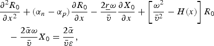
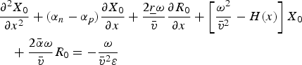
with
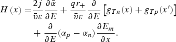
The integrated values of resistance and reactance give Z R and Z X using the relation

Using the values of Z R and Z X, the diode conductance (G), susceptance (B), and the quality factor (Q) are calculated using the relation

The expected RF power delivery from the diode can be computed using the relation

The power density, P A, is taken as P RF/A, where “A” is area of cross section of the device and has taken 10−10 m2 for the design frequency. V RF can be approximated as V B/2 for 50% modulation. G p is the device negative conductance at peak frequency [Reference Eisele, Haddad and Sze22]. The programs have been modified to incorporate diffusion/tunnel currents following methods reported elsewhere by our group.
C) Simulation technique for studying the avalanche noise
The fundamental avalanching process, involved in the IMPATT diode operation, leads to sufficient avalanche noise generation in the device. So noise is an important aspect of the present study and the noise characteristics of the diode structure are also computed using a generalized noise simulation program [Reference Pati, Tripathy and Dash23–Reference Reklaitis and Reggiani25]. The noise characteristics such as mean square noise voltage per bandwidth (<v 2 >/df) and noise measure of the device are computed from this analysis. The noise generation rate of the individual sources can be calculated by using the equation

The exact values of n, p, α n, and α p are determined from static analysis of the diode under avalanche breakdown condition, which also gives the distribution of electric field and the carrier concentration along the depletion layer of the diode [Reference Pati, Tripathy and Dash23].
The noise source α n(x′) is located at x′ in the avalanche region giving rise to noise electric fields (x, x′) at every point in the depletion region of the diode. The noise electric field (e(x, x′) = e R(x, x′) + ie X(x, x′)) contribution from each space point is calculated with the help of a double-iterative simulation program [Reference Pati, Tripathy and Dash23], which solves the following two second-order differential equations for the real e R(x, x′) and imaginary e X(x, x′) part of the noise electric field at each space point subject to the boundary conditions.
Now the following notations have been introduced:

Using the values of n and p and applying the above notation in equation (9), one can arrive at the following equation:

Now under small-signal condition, a small AC electric field  is super imposed on the DC electric field E m and let
 be the corresponding AC total current density.
Thus, applying small-signal condition and removing DC parts and neglecting higher-order terms in the small-signal part, the following equation is obtained:

with

separating equation (19) into real/imaginary components, we obtain

and

In a similar way, separating the real and imaginary parts, the boundary conditions on e R and e X are obtained as


Equations (18) and (19) on e R and e X are solved simultaneously subject to the boundary conditions (20) and (21), using a double-iterative computer developed on the basis of modified Runge–Kutta method [Reference Scarborough26]. The process is repeated by shifting the noise source to next space point progressively till the other edge point. The noise profile generated for particular location of the noise element can be obtained from the final solution through use of a self-converging double-iterative computer algorithm. Similarly, noise profiles are obtained by shifting the noise source to other points (x′) along the depletion zone. The total noise generated in the device can be computed through double integration (x and x′′).
The transfer impedance (Z T) of the diode is defined as the ratio of open circuit incremental voltage to the injected current at x′. Taking the injected current at x′ as dI N = qγN(x′)A dx′ [Reference Scarborough26, Reference Gummel and Blue27] with A being the area of cross section, one can obtain the real and imaginary parts of transfer impedance using the relation

The transfer impedance, mean square noise voltage, and noise measure are determined from the relations


where K is the Boltzmann constant, T is the junction temperature (taken to be 473 °K), and −Z R is the total negative diode resistance. The method is made free from numerical instability and is less time consuming through incorporation of a fast-converging logic.
III. RESULTS AND DISCUSSIONS
A) Comparison of high-frequency performances of SiC and GaN IMPATTs
Material and physical parameter of both the materials i.e. SiC and GaN of different poly-types are presented in Table 1. The design parameters of both SiC and GaN-based IMPATT diodes at 140 GHz are obtained through the optimization process. The other device properties such as breakdown voltage, efficiency, device negative conductance, expected RF power, mean square noise voltage per bandwidth, etc. at 140 GHz are presented in Table 2. The breakdown voltage (V B) for 4H-SiC IMPATT diode is found to be 180 V as compared with 170, 158, and 160 for 6H-SiC, ZB-GaN, and Wz-GaN, respectively. Since the breakdown voltage is indicative of input power of the device, the SiC and GaN are promising IMPATT diode materials for high-power operation. The breakdown electric field has been computed to be more i.e. 3.96 × 10⁸ V/m for Wz-GaN as compared with all materials. Figure 2(a) shows the electric field profile for both the material (SiC and GaN)-based DD IMPATTs. The estimated I–V plots of the designed diodes are shown in Fig. 2(b). The variation of negative conductance with frequency is plotted for hexagonal SiC (Fig. 3) and both the poly-types GaN (Fig. 4) IMPATT diode. On the other hand in ZB-GaN-based devices, the negative resistance is twice the Wz-GaN IMPATT diode. The negative resistivity profile of both the materials (Wz- and ZB-GaN) is shown in Fig. 5.
(a) Electric field profiles for SiC and GaN DD IMPATTs. (b) Estimated I–V plots of SiC and GaN DD IMPATTs.

Variation of negative conductance with frequency for SiC IMPATT diodes.

Variation of negative conductance with frequency for GaN IMPATT diodes.

Negative resistivity profile of GaN-based IMPATT diode.

Material parameters of SiC and GaN.

Mm-wave and noise properties of IMPATT diodes, with SiC and GaN as base materials, designed for operation at 140 GHz.

The negative conductance for both SiC and GaN diodes peaks at around 140 GHz that can be regarded as optimum frequency of operation of the diodes. The negative resistance contribution from individual space step is computed by taking the ratio e~/i~ in every individual space step in the final computer run. It is seen that the negative resistance profile along the depletion zone is of double peak nature with one peak remaining in each of the drift regions. The peak of negative resistance together with its spread along the active zones indicates contribution of negative resistance by individual space step. The avalanche zones, however, in the case of both the diodes produce positive RF resistance. The magnitude of peak of the negative resistance profile is higher in 4H-SiC diode than that for Wz-GaN diode. This leads to higher RF power generation from 4H-SiC device. These facts are reflected from Table 2 and Fig. 6, which indicate that the 4H-SiC DDR shows high-power density and thus 4H-SiC may have an advantage for being chosen as a base material for IMPATT diode. Recent study reported that as-grown Mg doped GaN layer has p-type conductivity with a concentration of ~3 × 1019 cm−3 [Reference Mukherjee, Mazumder and Roy28, Reference Usikov29]. This is much more improvement than the conventional values (1017–1018 cm−3). The highly doped p2+ cap layer is used to lower the contact resistance that in turn improves the high-power performance of IMPATTs. The authors have considered p2+ concentration ~1019 cm−3 and p-doping ~1017 cm−3, so these are realistic considerations, as far as present experimental observations are concerned. The authors have realistically estimated the parasitic resistances in the device, following Adlerstein's approach, including the effects of contacts [Reference Mukherjee, Mazumder and Roy28]. The contribution from un-depleted epitaxial layer, p, and n ohmic contacts are taken into account. The values of series positive resistance including ohmic contact are shown in Table 2.
Variation of RF power with frequency for SiC and GaN IMPATT diodes.

In order to draw a comparison, the authors also have studied the properties of silicon IMPATT DDR for the same frequency of 140 GHz. The RF power from silicon diode remains only around 0.32 W, which is nearly lower by a factor of around 25 than its 4H-SiC and Wz-GaN counterparts. The loss of power estimated owing to positive resistance also has been shown in Table 2. However, Wz-GaN has the advantage of producing low noise of about 0.74 × 10⁻¹⁵ V2 s as compared with 4H-SiC (5.16 × 10⁻¹⁵ V2 s) for IMPATT operation at 140 GHz. This can be inferred from Fig. 7, where the authors have plotted the variation of mean square noise voltage per band width versus frequency for IMPATT diodes based on both the poly-type SiC and GaN materials. This graph shows the transition frequency where the plots show peak. Based on a trade-off between the power output and noise from the device, it reveals that Wz-GaN would be a suitable base material for high-power application of IMPATT diode with moderate noise.
Variation of mean square noise voltage per bandwidth with frequency for SiC and GaN IMPATT diodes.

B) Fabrication issues related to GaN- and SiC-based IMPATTs
The computer simulation results show the importance and superiority of both the wide band gap materials (SiC and GaN) for high-power source at mm-wave regime. Special efforts have been made for the material growth, doping and device processing, oscillator performance, characterization of the device by taking the SiC and GaN as base materials for fabrication of the diode. Owing to the lack of experimental data on wide band gap semiconductor-based mm-wave devices, simulation results could not be compared. However, the authors have proposed the practical issues related to the fabrication of GaN and SiC IMPATT devices.
Considerable progress in the growth of nitrides during the last five years makes this material suitable for fabrication of various electronic devices [Reference Peatron, Zolper, Shul and Ren13, Reference Peatron14]. Recent experimental study [Reference Lee, Shin, Kim, Oh and Lim30] reveals the growth of high-quality GaN films on Si substrate by MOCVD technique by using a SixNy inserting layer. GaN p–n junction can be obtained by using the molecular beam epitaxy (MBE). In order to form a p–n junction, first, the MBE growth process can be carried out using Si donor impurity to form the n-type layer of GaN on an n+ substrate, and after that, a p+-type cap layer can be grown on the n-layer by the MBE process by doping high concentration of Mg impurity. In order to activate p-type conductivity, high-temperature post-growth anneal in a nitrogen atmosphere may be required. Because Mg requires large energy for ionization, in general, it is difficult to obtain heavily doped p+-type GaN with Mg. Beryllium (Be) may be used to achieve p+-type GaN because the ionization energy of Be is low (~60 meV). Recently, Pastor et al. [Reference Pastor, Ibáñez, Cuscó, Artús, González-Diaz and Calleja31] assessed the crystal damage of Be+-implanted GaN by UV Raman scattering and found a correlation between implantation dose and the extent of lattice damage caused to the target. GaN may be grown from the vapor phase using metal-organic gases as sources of gallium and nitrogen. For example, trimethylgallium can be used as a gallium source, and ammonia can be used as a nitrogen source. Growth of a GaN semiconductor may take place in a reactor chamber on a substrate. During the growth, the substrate may be kept at growth temperature ranging from 800 to 1100°C. Hence, in the light of the maturity of the fabrication technology and the unique material properties, GaN appears to be one of the best choices for the development of semiconductor devices for RF power, especially in THz region, in the coming decade for electronics communication.
A SiC IMPATT device can be fabricated on the epiwafer by following the process steps briefly described below [Reference Mukherjee, Mazumder and Roy28]. In order to assist p-type ohmic contact formation, the p+ SiC layer can be grown on top of the n-type film by Al2+ ion implantation. The post-implantation annealing may be performed at a very high temperature in an argon atmosphere. The power dissipation of IMPATT devices strongly depends on the contact resistance. The samples may be cleaned by a “piranha” solution. After rinsing in deionized water, the samples may be dipped in dilute hydrofluoric acid solution and dried for nearly 15 min. Through the lithographic process, windows can be opened inside the oxide layer. Using lithography and lift-off techniques, contact metals (Al/Ti/Al) can then be deposited in the oxide windows by an electron beam evaporator. In order to obtain ohmic contacts, the samples may be annealed for 3–5 min in a Rapid Thermal Anneal (RTA) furnace in nitrogen atmosphere at around 950°C. The post-deposition annealing at high temperature is generally preferred to reduce the specific contact resistance. For an n+- type contact, a Ni layer of 200-nm thickness may be evaporated on the backside (n+ side) of the wafer, followed by the RTA treatment for 3 min at 950°C [Reference Konishi, Yasokuchi, Nakatsuka, Koide, Moriyama and Murakami32]. The choice of the metallic composition is based on the formation of Ni2Si alloy. As mentioned in several publications [Reference Carter33], the higher the concentration of the Ni2Si in the contacts is, the lower the specific contact resistance is. The specific contact resistance can be determined from transmission line measurement data. The oxide layer from the p+ side can then be removed by a buffered oxide etch. Formation of a diode mesa using reactive ion etching (RIE): Si–C bonds show high chemical inertness; hence, wet etching is not efficient for reaching deep trenches. The more appropriate dry plasma etching, RIE, may be used in separating a diode mesa. A titanium/nickel (Ti/Ni) bilayer metal can be evaporated onto the sample. The depth and etch rate of the mask may be determined by profilemetry measurements with a Tencor Alpha Step. After finishing the fabrication process, on-wafer DC testing is performed before the diodes are packaged. DC testing may serve as the initial screening step of the devices, and the test results can be used for process evaluation. The packaging should provide a low thermal resistance between the SiC diode chip and waveguide mount and should be mechanically rugged and hermetically sealed. The device may be bonded to a pill-type package. Several experimental attempts have been taken for the development of SiC material for device fabrication [Reference Vassilevski, Zekmtas, Constantidis and Stel'chuck34–Reference Mukherjee, Mazumder and Dasgupta36].
However, experiments are in progress to realize SiC- and GaN-based high-power solid-state devices, the fabrication techniques should mature more to realize high power (Watts level) from those devices. Owing to the defects in epilayer growth of SiC and GaN devices, recombination of minority carrier may take place and it increases the leakage current and destroys the sharp nature of I–V characteristics, which in turn reduces power and efficiency. Again the unavailability of native substrate in GaN devices may form strain at the junction. This may generate a spontaneous strain field and that may degrade the value of peak electric breakdown field and consequently the IMPATT mode behavior of the devices.
IV. CONCLUSION
A detailed comparative analysis of both SiC- and GaN-based IMPATT diode at D-band has been reported by studying the DC, small-signal and avalanche noise analysis through the computer simulation technique, developed by the authors. It may be concluded that both SiC and GaN are potential materials for high-power IMPATT application. Wide gap associated with high breakdown voltage in both cases with tolerance to high operating current density would help in possible realization of high RF power. Both SiC and GaN diodes may yield an RF power 25–30 times higher than its Si counterpart. It is observed that for high-power operation the 4H-SiC is a suitable base material for IMPATT diode whereas Wz-GaN is a better material than 4H-SiC for high-power operation with moderate noise. To the best of authors' knowledge this is the first report on the comparative analysis of mm-wave characteristics and avalanche noise analysis of both hexagonal-type SiC and both poly-types GaN IMPATTs at an important window frequency of 140 GHz. This study will be useful for practical realization of high-power, low-noise IMPATT in the mm-wave region used for electronics communication.
ACKNOWLEDGEMENTS
Moumita Mukherjee is grateful to Defence Research and Development Organisation (DRDO), Ministry of Defence, Govt. of India for providing her “Research associateship” to carry out this research work. Prof Pati wishes to express his sincere thanks to AICTE, New Delhi for grant of Emeritus Fellowship in his favor.
 Pravash Ranjan Tripathy completed Master Degree in Electronics from Sambalpur University in the year 2001. Presently he is working as an Assistant Professor and Head of the Department of Electronics and Telecommunication Engineering, Purushottam Institute of Engineering & Technology (PIET), Rourkela, Odisha. He has published more than 40 research papers in international Journals/conferences proceeding. He is the Member of IEEE (USA), IEEE-ED society, IEEE-MTTs and Life member of OPS. His research interests include development of computer models for high-frequency millimeter- and Sub-millimeter-wave devices, design and modeling of high-performance IMPATT oscillators for RF communication.
 Moumita Mukherjee is attached with Centre for Millimeter wave Semiconductor Devices and Systems (CMSDS, a centre of DRDO, Ministry of Defence, Govt. of India, and University of Calcutta), as Scientist – B (Senior Assistant Professor grade). Her research interests include the design and fabrication of millimeter- and submillimeter- (Terahertz) wave high-power devices based on wide-band gap semiconductors and the study of photo irradiation effects on high-power MM-wave and Terahertz IMPATT oscillators. She is presently working on the modeling of nanoscale transit time devices for generation of THz oscillations. She has published more than 100 peer-reviewed research papers and 8 books/invited book chapters on semiconductor devices in several reputed international journals and IEEE- proceedings.
Ms. Mukherjee is a member of IEEE (USA) and IEEE-ED society (USA).
 Shankar Prasad Pati was a former professor in the Department of Physics/Electronics, Sambalpur University, Odisha and is now working as an Emeritus professor (AICTE) in NIST Berhampur, Odisha. He has published more than 120 International Journals and more than 250 International and National conferences. He is a Fellow member of IETE, IMS and Orissa Physical Society. He has received Samanta Chandra Sekhara award for his outstanding contribution in Science & Engineering from Government of Odisha. His research interest is Microwave Semiconductor Devices.



