Introduction
π-conjugated polymers have gained great significance over the past two decades as solution-processable semiconductors in the next generation optoelectronics.[ Reference Facchetti 1 – Reference Himmelberger, Duong, Northrup, Rivnay, Koch, Beckingham, Stigelin, Segalman, Mannsfeld and Salleo 7 ] Unlike inorganic-based materials currently used in mainstream optoelectronic devices, polymeric semiconductors offer advantageous rheological properties, which allows the fabrication of electro-active ink formulations for high-throughput manufacturing process by printing on light-weight, large-area, and flexible plastic substrates.[ Reference Kumar, Kaushik and Negi 8 – Reference Baeg, Khim, Kim, Kang, You, Kim and Noh 16 ] In addition, the chemical structure of the polymer π-backbone and substituents can be easily tuned via synthetic organic chemistry. This offers considerable flexibility for device fabrication and functionalities by tuning opto-electronic responses and processing characteristics.[ Reference Fukutomi, Nakano, Hu, Osaka and Takimiya 17 , Reference Sinha, Lee, Kong, Swift and Katz 18 ] Therefore, with the aim of realizing a new generation of low-cost, large-area, flexible electronics, polymeric semiconductors have been extensively studied in organic thin-film transistors (OTFTs),[ Reference Li, Sonar, Singh, Soh, van Meurs and Tan 19 – Reference Ryu, Park, Park, Kim and Noh 22 ] organic light-emitting diodes (OLEDs),[ Reference So and Kondakov 23 – Reference Aizawa, Pu, Chiba, Kawata, Sasabe and Kido 25 ] and organic photovoltaic cells (OPVs),[ Reference Dang, Hirsch, Wantz and Wuest 26 – Reference Yasuda, Kuwabara, Han and Kanbara 29 ] and have recently emerged in organic light-emitting transistors (OLETs).[ Reference Ullah, Tandy, Yambem, Aljada, Burn, Meredith and Namdas 30 – Reference Usta, Sheets, Denti, Generali, Capelli, Lu, Yu, Muccini and Facchetti 32 ] Since the initial report on electrochemically grown polythiophene as the active layer in OTFTs,[ Reference Tsumura, Koezuka and Ando 33 ] the development of semiconducting polymers with a high charge-carrier mobility has dramatically progressed by design and synthesis of new π-backbone architectures, and improvements on polymer thin-film microcrystallinity/morphology.[ Reference Lee, Lee, Shin, Cho and Choi 34 ] In principle, charge transport in a semiconducting polymer thin-film relies on two processes: intra-chain charge transport through polymer π-backbone, and interchain charge hopping between π − π stacked adjacent chains.[ Reference Pan, Li, Wu, Liu, Ong, Zhu and Xu 35 ] Typically, both processes operate although film morphology tuning can alter the major transport characteristics. Therefore, optimized π-extended/delocalized polymer backbone architectures, and favorable thin-film texturing and morphology are crucial to achieve high charge-carrier mobilities. To this end, a large number of semiconducting polymers embedding various π-electron-rich and -deficient monomers have been developed, and OTFT charge-carrier mobilities reliably reaching commercially relevant values (~0.5–1.0 cm2V−1s−1) have been achieved.[ Reference Lei, Dou and Pei 36 , Reference Mei, Kim, Ayzner, Toney and Bao 37 ] Furthermore, very recently, breakthrough OTFT performances with mobilities more than 3.0 cm2V−1s−1 have been achieved.[ Reference Li, Zhao, Tan, Guo, Di, Yu, Liu, Lin, Lim and Zhou 14 , Reference Yuan, Giri, Ayzner, Zoombelt, Mannsfeld, Chen, Nordlund, Toney, Huang and Bao 21 , Reference Gao and Zhao 38 – Reference Tseng, Phan, Luo, Wang, Perez, Patel, Ying, Kramer, Nguyen, Bazan and Heeger 43 ] Our group has previously demonstrated an air-stable solution processable n-channel polymer, P(NDI2OD–T2) (Polyera ActivInk™, N2200), consisting of a naphthalenediimide (NDI) acceptor unit and a bithiophene donor moiety, which can exhibit excellent electron mobilities in ambient up to ~0.45–0.85 cm2V−1s−1 in conventional top-gate/bottom-contact (TG/BC) device architectures,[ Reference Yan, Chen, Zheng, Newman, Quinn, Dötz, Kastler and Facchetti 44 ] and ~3 cm2V−1s−1 for Ba-modified electrical contacts.[ Reference Kim, Khim, Xu, Lee, Kang, Kim, Facchetti, Noh and Kim 45 ] The ambient stability of these OTFTs was attributed to polymer's stabilized lowest unoccupied molecular orbital (LUMO) energy level (−3.96 eV) and to the encapsulation effect of the top dielectric layer.[ Reference Chen, Zheng, Yan and Facchetti 46 ] Following our initial report, numerous studies have been performed either on further optoelectronic characterization of P(NDI2OD–T2) or on the development of different NDI-based polymer semiconductors.[ Reference Chen, Guo, Mao, Yu, Huang, Zhao and Liu 47 , Reference Kim, Amegadze, Kang, Yun, Noh, Kwon and Kim 48 ] In these studies, excellent semiconductor performances have been achieved in OTFT and OPV devices, and key structure–property–function relationships have been elucidated to provide the basis for fundamental understanding of electron transport in polymer thin films.[ Reference Guo, Facchetti and Marks 49 ] These results indicate that P(NDI2OD–T2) and its derivatives are very promising in the field of polymer optoelectronics, where stable and efficient electron transport is required, and they should be explored more in terms of structural modification and device optimization.
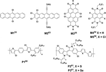
To a first approximation, the stability of injected/induced electrons in semiconducting polymers during n-channel transport is governed by the LUMO energy level through which charge transport occurs,[ Reference Usta, Kim, Wang, Lu, Huang, Facchetti and Marks 50 , Reference Jones, Facchetti, Wasielewski and Marks 51 ] with several strudies suggesting that a LUMO energy level <−4.0 eV is required to stabilize n-channel transport against ambient/surface traps.[ Reference Anthopoulos, Anyfantis, Papavassiliou and de Leeuw 52 ] In this regard, we envision that further functionalization of the P(NDI2OD–T2) polymer backbone with chlorine substituents may afford novel physicochemical and optoelectronic properties, and further extend its application in optoelectronic devices. Rational chlorination on the π-backbone of P(NDI2OD–T2) should further stabilize π-energy levels and improve ambient-stability. Although, in recent years, a number of chlorinated small molecules, including dichloropentacene M1 and tetrachlorotriisopropylsilyl (TIPS)-acetylene pentacene M2, tetrachloroperylenediimide M3, and dichloro (M4) and tetrachloro (M5) naphthalene diimides (Fig. 1) have been reported as high mobility p/n-channel semiconductors in OTFTs,[ Reference Wang, Li, Zhao, Wu, Huang, Hu, Gao, Li and Zhu 53 – Reference Yamada, Okujimaa and Ono 58 ] chlorination strategy has not been broadly applied to polymer semiconductors.[ Reference Li, Meng, Tong, Xie and Wang 59 ]
Structures of representative chlorinated π-conjugated small molecules (M1–M5) and polymers (P1–P3) for OTFTs.

For example, P1 is one of the early examples of chlorinated π-conjugated polymers, and isoindigo-based polymers P2 and P3 (Fig. 1) are the only examples of chlorinated semiconductors reported in the literature with good OTFT performance in ambient.[ Reference Xu, Ng and Chan 60 , Reference Lei, Dou, Ma, Liu, Wang and Pei 61 ] Since the Cl atom has a relatively lower electronegativity compared with the well-studied F atom [Pauling electronegativity[ Reference Allred 62 ] = 3.16 (Cl) and 3.98 (F)], the LUMO energy reduction of π-conjugated systems has been attributed to the delocalization of π-electrons into the unoccupied 3d orbitals of Cl.[ Reference Tang, Oh, Reichardt and Bao 63 ] Similar π-delocalization is not energetically favorable for other electron-withdrawing functionalities such as fluorine (–F) and cyano (–CN). Furthermore, when π-backbones of polymers are substituted with chlorine, their solubilities in common organic polar solvents should increase due to enhanced polarizability of –Cl compared with those of –H and –F.[ Reference Oh, Suraru, Lee, Könemann, Höffken, Röger, Schmidt, Chung, Chen, Würthner and Bao 56 ]
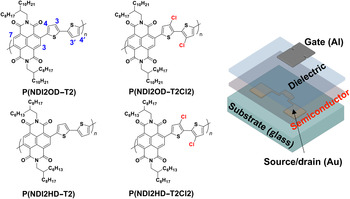
To the best of our knowledge, an NDI-based polymer with chlorine substituents on the π-backbone has never been reported in the literature. In this study, we designed, synthesized, and characterized two new chlorinated polymeric semiconductors, P(NDI2HD–T2Cl2) and P(NDI2OD–T2Cl2), embedding the NDI acceptor unit with 2-hexyldecyl (2HD) or 2-octyldodecyl (2OD) N-substituents, and a 3,3′-dichloro-2,2′-bithiophene (T2Cl2) co-monomer. We also compared their optoelectronic and OTFT device properties to the corresponding chlorine-free analogs of similar molecular weights (Fig. 2). Our results suggest that the electronic structure of the new polymers are affected by chlorine substitution, resulting in far larger band gap (1.69 versus 1.45 eV), and lower highest occupied molecular orbital (HOMO) (−5.73 eV versus −5.34 eV) and LUMO (−4.04 versus −3.89 eV) energy systems. TG/BC thin-film transistors fabricated with the new polymers exhibit n-channel behavior in ambient with electron mobilities up to 0.06 cm2V−1s−1 and current on/off ratios of up to 106–107. Compared with those fabricated with non-chlorinated P(NDI2OD–T2), the new devices exhibit largely improved thin-film transistor (TFT) device stabilities when stored under high humidity (RH ~ 60%), and they function in water, opening possibilities for further implementation of these polymers into new device structures and functions.
Chemical structures of the polymers and schematic of a TG/BC TFT architecture used in this study.

Experimental section
Materials and methods
All reagents were purchased from commercial sources and used without further purification unless otherwise noted. The reagents 3,3′,5,5′-tetrachloro-2,2′-bithiophene, 2,6-dibromonaphthalene-1,4,5,8-tetracarboxydianhydride (NDA-Br2), N,N′-bis(2-hexyldecyl)-2,6-dibromonaphthalene-1,4,5,8-bis(dicarboximide) (NDI2HD-Br2), N,N′-bis(2-octyldodecyl)-2,6-dibromonaphthalene-1,4,5,8-bis(dicarboximide) (NDI2OD-Br2), 2-hexyldecylamine,2-octyldodecylamine, 5,5′-bis(trimethylstannyl)-2,2′-bithiophene and the non-chlorinated polymers P(NDI2HD–T2), and P(NDI2OD–T2) were prepared according to literature procedures.[ Reference Kim, Kang, Dutta, Han, Shin, Noh and Yang 39 , Reference Letizia, Salata, Tribout, Facchetti, Ratner and Marks 64 – Reference Chaignon, Falkenström, Karlsson, Blart, Odobel and Hammarström 66 ] 1H NMR spectra were obtained using an Inova 500 (500 MHz) NMR spectrometer. Elemental analyses were performed by Midwest microlab, LLC. Polymer molecular weights were determined on a Polymer Laboratories PL-GPC 220 using trichlorobenzene as eluent at 150 °C versus polystyrene standards. Electrochemical measurements were carried out using Epsilon Electrochemical Workstation equipped with BAS Epsilon software (Bioanalytical Systems, Inc., Lafayette, IN) in a 3-electrode cell configuration (VC-2 voltammetry cell), using 1.0 mm diameter platinum disk working electrode and a platinum wire counter electrode, and Ag wire was used as the pseudo-reference electrode. Polymer sample films were deposited onto the working electrode by drop-casting. Cyclic voltammetry measurements were performed in 0.1 m tetrabutylammonium hexafluorophosphate (Bu4N+PF6 –) acetonitrile solution at a scan rate of 50 mV/s. Ferrocene/Ferrocenium (Fc/Fc+, 0.54 V versus SCE) was used as an internal reference for all measurements. Optical absorption spectra were obtained on thin films (~30 nm on glass) with a Cary 50 Scan UV-Visible Spectrometer. E LUMO is calculated as:—(E red−1 + 4.44 eV) assuming that Koopmans' theorem holds (EA red ≈ −E LUMO). SCE energy level is taken to be −4.44 eV below the vacuum level. E HOMO is calculated from: HOMO = LUMO − E g (estimated from optical absorption spectra).[ Reference Bard and Faulkner 67 ]
Synthesis of T2Cl2 (1)
Under argon, a mixture of 3,3′,5,5′-tetrachloro-2,2′-bithiophene (3.04 g, 10.0 mmol), zinc powder (1.95 g, 30.0 mmol), isopropylalcohol (50 mL), and acetic acid (15 mL) was refluxed for 24 h. After thin-layer chromatography test indicated the incompletion of reaction, more zinc powder (1.44 g, 22.2 mmol) and acetic acid (12 mL) was added and the reaction mixture was stirred under nitrogen for an additional 38 h. Upon cooling to room temperature, the reaction mixture was precipitated in methanol, and the crude product was subject to column chromatography on silica gel to afford a white solid as the product (0.27 g, 11.5%). 1H NMR (CD2Cl2, 400 MHz): δ 7.43–7.44 (d, J = 5.2 Hz, 2H), 7.04–7.05 (d, J = 5.2 Hz, 2H).
Synthesis of 5,5′-bis(trimethylstannyl)-T2Cl2 (2)
Under argon, a solution of T2Cl2 (0.26 g, 1.1 mmol) in anhydrous tetrahydrofuran (THF) (15 mL) was cooled to −78 °C, and a solution of n-BuLi in hexane (0.90 mL, 2.24 mmol) was then added dropwise. The resulting solution was stirred at this temperature for about 30 min and at room temperature for an additional 1 h. The reaction mixture was then cooled to −78 °C again, and a solution of trimethyltin chloride (4.5 mL, 1 m in hexane, 4.5 mmol) was added slowly. This mixture was allowed to warm to room temperature and stirred at room temperature overnight. After the reaction was diluted with hexane (~100 mL), it was washed with water (3 × 30 mL), dried over anhydrous sodium sulfate, and concentrated in vacuo. The residue was recrystallized from isopropyl alcohol, leading to a pale solid as the product (0.39 g, 63.2%). 1H NMR (CDCl3, 400 MHz): δ 7.03 (s, 2H), 0.40 (m, 18H).
Synthesis of P(NDI2HD–T2Cl2)
Under argon, a mixture of NDI2HD-Br2 (669.1 mg, 0.77 mmol), 5,5′-bis(trimethylstannyl)-T2Cl2 (2) (430.5 mg, 0.77 mmol), Pd2dba3 (14.1 mg, 0.015 mmol), and P(o-tol)3 (37.5 mg, 0.12 mmol) in anhydrous chlorobenzene (60 mL) was stirred at 90 °C for 18 h. Bromobenzene (0.5 mL) was then added, and the resulting mixture was stirred for an additional 6 h. After cooling to room temperature, the reaction mixture was poured into methanol (200 mL). The resulting suspension was stirred for 20 min, before the precipitate was collected by filtration and washed with methanol. This crude product was then subjected to Soxhlet extraction under nitrogen with methanol, acetone, and hexane. Finally, it was extracted with chlorobenzene (about 200 mL). Upon cooling to room temperature, the chlorobenzene extract was precipitated into methanol (400 mL). The precipitate was collected by filtration, washed with methanol, and dried under vacuum, leading to a dark solid (675.0 mg, 93.1%). 1H NMR (CDCl2CDCl2, 500 MHz, 120 °C): δ 8.91 (s, 2H), 7.40 (s, 2H) , 4.22 (s, br, 4H), 2.12 (s, br, 2H), 1.25–1.56 (m, br, 48H), 0.89–0.97 (m, br, 12H).GPC: M n = 20.4 kDa, PDI = 2.2. Elemental Analysis (calc. C, 68.55; H, 7.46; N, 2.96): found C, 68.44; H, 7.41; N, 3.01.
Synthesis of P(NDI2OD–T2Cl2)
Under argon, a mixture of NDI2OD-Br2 (655.3 mg, 0.67 mmol), 5,5′-bis(trimethylstannyl)-T2Cl2 (2) (373.0 mg, 0.67 mmol), Pd2dba3 (12.2 mg, 0.013 mmol), and P(o-tol)3 (32.4 mg, 0.11 mmol) in anhydrous chlorobenzene (60 mL) was stirred at 90 °C for 20 h. Bromobenzene (0.5 mL) was then added, and the resulting mixture was stirred for an additional 5 h. After cooling to room temperature, the reaction mixture was poured into methanol (150 mL). The resulting suspension was stirred for 20 min, before the precipitate was collected by filtration and washed with methanol. This crude product was then subject to Soxhlet extraction under nitrogen with methanol, acetone, and hexane. Finally, it was extracted with chlorobenzene (about 350 mL). Upon cooling to room temperature, the chlorobenzene extract was precipitated into methanol (500 mL). The precipitate was collected by filtration, washed with methanol, and dried under vacuum, leading to a dark solid (687.2 mg, 96.9%).1H NMR (CDCl2CDCl2, 500 MHz, 130 °C): δ 8.92 (s, 2H), 7.41 (s, 2H) , 4.23 (s, br, 4H), 2.13 (s, br, 2H), 1.26–1.58 (m, br, 64H), 0.88–0.99 (m, br, 12H). GPC: M n = 17.0 kDa, PDI = 1.8. Elemental Analysis (calc. C, 70.36; H, 8.19; N, 2.65): found C, 70.59; H, 8.28; N, 2.81.
TFT device fabrication and measurements
OTFTs with TG/BC architecture were fabricated on Corning Eagle 2000 glass substrates. The source–drain (S/D) electrodes were thermally evaporated Au contacts (40 nm thick) with L = 50 µm and W = 1 mm (for the devices of Table II) or photolithography-defined Ni (3 nm)/Au (13 nm) with L = 2–60 µm and W = 1 mm (for contact resistance measurements and devices presented in Table III). The defined substrates were cleaned in an ultrasonic bath with acetone, isopropanol, and de-ionized water, respectively (10 min each), and then post-baked at 110 °C for 30 min. N-channel polymer semiconductor formulations of P(NDI2HD–T2Cl2) and P(NDI2OD–T2Cl2) were prepared by dissolving the corresponding polymers in anhydrous dichlorobenzene at 1, 5, and 10 mg/mL concentrations. The non-chlorinated parent polymers, P(NDI2HD–T2) and P(NDI2OD–T2) (Polyera ActivInk™ N2200) were dissolved in p-xylene to obtain 10 mg/mL reference semiconductor solutions. The semiconductor solutions were filtered through 0.2 µm polytetrafluoroethylene syringe filter, and spin-coated at 2000 rpm for 60 s in an N2-filled glove box. The spin-coated P(NDI2HD–T2Cl2) and P(NDI2OD–T2Cl2) films were thermally annealed at 150 °C for 30 min and 110 °C for 20 min, respectively, in a glove box with a N2 atmosphere to remove residual solvents. Poly(methyl methacrylate) (PMMA) (Aldrich, M W = 120 kDa) or a CYTOP solution (Asahi) ware used as the dielectric material. PMMA was dissolved in n-butylacetate to obtain 80 mg/mL dielectric solution, and it was spin-coated at 2000–3000 rpm for 60 s on the semiconducting polymer film. Afterwards, the devices were baked at 80 °C for 2 h to remove residual solvent under N2. The OTFTs were completed by depositing Al TG electrodes via thermal evaporation with the aid of metal shadow mask. The fundamental OTFT electrical characteristics were measured using a Keithley 4200 semiconductor characterization system in an N2-filled glove box. The conventional saturation mobility (μ sat) and corresponding V Th were extracted at the saturation region (at a drain voltage V DS of +80 V) using gradual channel approximation equation for a standard metal oxide semiconductor TFT (MOSFET): μ sat = (2I DS L)/[WCi(V G−V Th)2], where I DS is the S/D saturation current, C i is the gate dielectric capacitance (per area), and V G is the gate voltage.
Results and discussion
Computational modeling
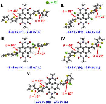
Chlorine incorporation into the parent polymers P(NDI2HD–T2) and P(NDI2OD–T2) was motivated by the aforementioned electronic and solubility advantages. However, the regiochemistry of the substitution must take into account the synthetic strategy and the far larger Van der Waals radius of Cl (1.75 Å) versus H (1.20 Å) and F (1.47 Å) to avoid sterically congested π-backbone distortions between NDI acceptor and bithiophene donor units. Thus, geometry optimizations and molecular orbital (MO) computations on several polymer segments (model structures I–V) incorporating chlorine atoms at different locations were performed at the DFT level to guide the polymer design. Figure 3 and S1 collect the computed structures, MO topologies and energies, and relevant torsional angles (θ) for the model units I–V. The computed MO energies (E H = 5.43 eV and E L = −3.31) and θ values (θ NT = 46° and θ TT = 19°) for the unsubstituted system (structure I) are in agreement with previous computations on similar backbones. Note, it was found experimentally that NDI-based polymers such as P(NDI2OD–T2) exhibit a torsional angle of ~35° between the NDI and the T2 units, which does not prevent efficient electron transport.[ Reference Zhan, Facchetti, Barlow, Marks, Ratner, Wasielewski and Marder 68 , Reference Jones, Ahrens, Yoon, Facchetti, Marks and Wasielewski 69 ] Our geometry optimizations indicate that chlorine functionalization at both NDI 3,7- (structure II) and thiophene 4-positions (structure III) considerably increases the NDI-T interring torsional angles (θ NT) to 68° and 64°, respectively. In all cases, the interring torsional angles between the two adjacent thiophene units (θ TT) are similar (18–23°). However, when the chlorine atoms are introduced at the 3-positions of the thiophenes on both sides of NDI (structure IV) or at the 3,3′-positions of the bithiophene moiety (structure V), θ NT values are identical to those of the unsubstituted systems (45–46°), which is critical to maintain a good donor–acceptor (D–A) electronic communication in the polymer backbone. The thiophene–thiophene torsional angle, θ TT, is unaffected for the structure IV having one chlorine at either side (22°), whereas it increases to ~63° in the case of the head-to-head 3,3′-dichloro substituted structure V. It is noteworthy that the addition of chlorine substituents into the polymer π-backbone may induce intrachain (thienyl)Cl···S(thienyl) and interchain (thienyl)Cl···O(imide), non-covalent interactions,[ Reference Ji, Xia, Ren, Wang, Wang and Diao 70 , Reference Adhikari and Scheiner 71 ] which could promote rigidification and solid state stacking. Chlorine incorporation also affects the frontier MO energies of the structures I–V. Considering the MO topologies (Fig. S1) with the LUMO localized on the NDI acceptor and the HOMO more delocalized along the thiophene units, Cl insertion on the NDI unit generally more effectively reduces the LUMO energy (−3.53 eV) versus the parent structure I (−3.31 eV), whereas this effect is weaker for structures III and V. On the other hand, the HOMO level is found to be effectively stabilized (Δ = 0.23 eV) in structure V since chlorine substitution is on the donor bithiophene moiety. Considering the synthetic accessibility, acceptable NDI-Thiophene interring torsional angle, and regioregularity of the monomers, structure V was selected for the synthesis of the new chlorinated polymers.
Computed molecular structures of polymer model structures I–V based on NDI-thiophene.

Synthesis of monomers and polymers
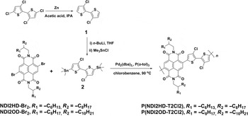
Scheme 1 shows the synthesis of the chlorinated bithiophene monomer 2, and the corresponding copolymers P(NDI2HD–T2Cl2) and P(NDI2OD–T2Cl2). The building block 2 was prepared from 3,3′,5,5′-tetrachloro-2,2′-bithiophene via a sequence of reactions involving selective dehalogenation and lithiation/stannylation. Although enough amount of 2 was obtained in high purity, it is noteworthy that the yield over two steps was found to be <10%, which may be attributed to poor selectivity of dechlorination and the formation of decomposition products.[ Reference Chan, Ng, Seowa and Moderscheimb 72 ] The syntheses of N,N-dialkylated 2,6-dibromonaphthalene diimides, NDI2HD-Br2 and NDI2OD-Br2,were performed according to literature procedures (see Supporting Information), and they were purified by column chromatography. Two different alkyl substituents, 2HD and 2OD, were used to record the effects of alkyl substituents on polymer processibility and optoelectronic properties. The chlorinated polymers, P(NDI2HD–T2Cl2) and P(NDI2OD–T2Cl2) were synthesized via conventional Stille polycondensation protocols by reacting the chlorinated bithiophene monomer 2 with NDI2HD-Br2 and NDI2OD-Br2, respectively, in chlorobenzene using Pd2(dba)3/P(o-tol)3 as the catalyst/ligand system. The new polymers were found to be soluble in common non-protic organic solvents including THF, toluene, xylenes, chloroform, and chlorobenzene, and they were purified by sequential soxhlet extractions and multiple dissolution–precipitation processes (93–97% yields). The observed high yields for the polymerization reactions are consistent with the previous reports on different NDI polymerizations, and it indicates the favorable structural/electronic properties of the present monomers for effective Pd-mediated coupling reactions.[ Reference Guo, Kim, Seger, Jenekhe and Watson 73 ] The final polymer structures and purities were characterized by 1H NMR spectroscopy, elemental analysis, and gel permeation chromatography. The number average molecular weights (Mn's) of the new chlorinated polymers were determined to be 20.4 kDa (PDI = 2.2) for P(NDI2HD–T2Cl2) and 17.0 kDa (PDI = 1.8) for P(NDI2OD–T2Cl2). To better understand the effects of chlorination on NDI-based polymers without any contribution from molecular weight differences, the non-chlorinated polymers, P(NDI2HD–T2) and P(NDI2OD–T2), were also synthesized with comparable number average molecular weights of 18.5 kDa (PDI 1.9) and 28.6 kDa (PDI = 2.2), respectively.
Synthesis of chlorinated bithiophene monomer 2, and the corresponding chlorinated polymers, P(NDI2HD–T2Cl2) and P(NDI2OD–T2Cl2).

Optical and electrochemical properties of polymers
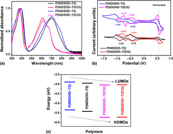
The optical absorption and electrochemical redox properties of the new chlorinated polymers along with the non-chlorinated parent polymers were investigated by thin-film UV–vis absorption and cyclic voltammetry measurements. The optical spectra and voltammograms are shown in Fig. 4, and data are collected in Table I. P(NDI2HD-T2Cl2) and P(NDI2OD–T2Cl2) exhibit two main absorptions corresponding to the π − π* and D–A intramolecular charge transfer (ICT) transitions of the naphthalene diimide–dichlorobithiophene backbone, which are located at λ max = 376/613 nm and λ max = 371/607 nm, respectively (Fig. 4(a)).
(a) Optical absorption spectra of spin-coated P(NDI2HD–T2Cl2) (magenta), P(NDI2OD–T2Cl2) (red), P(NDI2HD–T2) (blue), and P(NDI2OD–T2) (black) films (~30 nm thick) on glass. (b) Thin-film cyclic voltammetries of (NDI2HD–T2Cl2) (magenta), P(NDI2OD–T2Cl2) (red), P(NDI2HD–T2) (blue) and P(NDI2OD–T2) (black) thin films on a Pt working electrode [Fc/Fc+ (0.54 V versus SCE) as an internal standard]. (c) HOMO/LUMO energy levels for the present chlorinated and non-chlorinated NDI-based copolymers.

Physicochemical properties [molecular weight (Mn, kD), polydispersity (PDI), film optical absorption maxima (λ max film, nm), energy gaps (Egopt, eV), electrochemical reduction potentials (E 1/2 red,V), and HOMO/LUMO energy levels (eV)] of polymers P(NDI2HD–T2Cl2), P(NDI2OD–T2Cl2), P(NDI2HD–T2), and P(NDI2OD–T2).

a From optical absorption as spin-coated thin film on glass, optical band gap is estimated from the low-energy band edge of the UV–vis spectrum.
b As thin film with 0.1 m Bu4N+PF6 − in acetonitrile (versus SCE).
c E HOMO is calculated from E g opt = E LUMO − E HOMO.
d Estimated from the equation E LUMO = −4.44 eV − E 1/2 red−1.
Both the low-energy and high-energy maxima are shifted to shorter wavelengths by ~13–92 nm versus those of their parent non-chlorinated polymers P(NDI2HD–T2) (λ max = 389/700 nm) and P(NDI2OD–T2) (λ max = 392/699 nm). The corresponding optical band gaps (E g's) are estimated from the low-energy band edges as 1.69 eV for P(NDI2HD–T2Cl2), 1.69 eV for P(NDI2OD–T2Cl2), 1.45 eV for P(NDI2HD–T2) and 1.47 eV for P(NDI2OD–T2). The observed band gap increases for the present chlorinated NDI polymers is consistent with the hypochromic shifts in the absorption maxima. However, the absorption shifts upon chlorination on the lower energy maxima are more profound (∆λ max = 87–92 nm) compared with those of high energy maxima (∆λ max = 13–21 nm). This result may be attributed to the different origin of these transitions, and how they are affected by the chlorine substitutions. Since ICT band is affected by the strength of D–A coupling in the polymer backbone, the weaker donor character of the T2Cl2 unit versus T2 reduces D–A interactions.[ Reference Anthopoulos, Anyfantis, Papavassiliou and de Leeuw 52 ] On the other hand, the π − π* transition is mostly governed by the extent of π-conjugation. Since the polymer backbone in NDI-bithiophene polymers is already twisted, the larger steric demand of Cl versus H may slightly reduce the backbone planarity on the bithiophene moiety, as supported by the MO computations. This reduces the π-conjugation length and increases the π − π* transition energies.[ Reference Li, Vamvounis and Holdcroft 74 – Reference de Oliveira, Camilo, da Silva-Filho and Lavarda 76 ] Although the nature of the N-alkyl substituent (2HD versus 2OD) is found to have negligible effects on the polymer absorption maxima and band gap, slight differences were observed in peak vibronic features, which are possibly due to different polymer chain packings in the solid-state.
Cyclic voltammetry measurements provide further insights into the redox properties and energy level changes of the new chlorinated polymers. Two reversible reductions [Fig. 4(b)] are observed for both P(NDI2HD–T2Cl2) and P(NDI2OD–T2Cl2) with the first/second reduction potentials located at −0.40/−0.73 V and at −0.41/−0.75 V, respectively. The reversibility of both reductions demonstrates the redox stability of the new chlorinated polymer backbone. The reduction potentials exhibit anodic shifts compared with those of non-chlorinated polymers [P(NDI2HD–T2) = −0.55/−1.04 V and P(NDI2OD–T2] = −0.49/−0.96 V) when measured in the same electrochemical set-up. This is consistent with the stronger electron-withdrawing characteristics of –Cl compared with –H (vide supra), which facilitates the reduction processes. In addition, chlorine functionalization at NDI-T2 backbone decreases the voltage gap between the first two reductions (E 1/2 red−1 − E 1/2 red−2) by 0.2 V, further supporting the more electron-accepting nature of these derivatives, which renders the second reduction more facile.
Based on solid-state optical and electrochemical data, the HOMO/LUMO energies are estimated as −5.73/−4.04 eV for P(NDI2HD–T2Cl2) and −5.72/−4.03 eV for P(NDI2OD–T2Cl2). The HOMO and LUMO energy levels of the new chlorinated polymers are ~0.1–0.4 eV lower than those of parent non-chlorinated polymers, P(NDI2HD–T2) (−5.34/−3.89 eV) and P(NDI2OD–T2) (−5.42/−3.95 eV).[ Reference Lei, Dou and Pei 36 ] The reduction of the LUMO energies (ΔE LUMO = 0.1–0.15 eV) is less pronounced than those of the HOMO energies (ΔE HOMO = 0.3–0.4 eV), in agreement with the electronic structure of these polymers. This result is mainly because the LUMO is primarily localized on the NDI acceptor unit whereas the HOMO is more delocalized toward the bithiophene units where the chlorine atoms are located (Fig. S1). The lower LUMO energy level of the present polymers is expected to stabilize the field effect-induced electrons, while the far reduced HOMO energy should reduce the ambipolar characteristics when using certain dielectrics.[ Reference Kim, Hong, Oh and Yang 77 ] The interesting question is how the considerably decreased NDI–T2 intramolecular electronic coupling and slightly reduced π-conjugation will affect charge transport in OTFTs.
Charge transport measurements
The comparative charge transport properties of the new NDI-based copolymers were investigated in TG/BC transistor geometries. The experimental details are described in the Supporting Information. Briefly, thermally evaporated Au contacts (40 nm) or photolithography-defined Ni (3 nm)/Au (13 nm) were used as the S/D electrodes (L = 2–60 µm; W = 1 mm). The polymer semiconducting layers were deposited by spin-coating 1–10 mg/mL formulations in 1,2-dichlorobenzene or xylene for 1 min, and the films were annealed at 100–300 °C for 30 min. Next, the polymeric dielectric layer (PMMA or CYTOP) was spin-coated, and the devices were annealed to remove residual solvents and induce thin-film ordering. The OTFT devices were completed by depositing 50 nm thick Au or Al TG electrodes via thermal evaporation using a shadow mask. Device characteristics were evaluated under positive or negative gate bias in ambient conditions to explore the majority charge carrier type and device performance. The device carrier mobilities (μ) were calculated both in the linear and saturation regimes using conventional MOSFET equations.
In preliminary experiments, the OTFT characteristics of the chlorinated polymers were investigated with respect to the semiconductor solution concentration and semiconductor film post-deposition annealing temperature (Table S1, Supporting Information). Three different semiconductor solution concentrations (1, 5, and 10 mg/mL) were used resulting in three different active layer thicknesses of ~12, 17, and 23 nm, respectively. In addition, thermal annealing at four different temperatures (100, 150, 200, and 300 °C) were also explored. The output curves reveal the existence of some degree of contact resistance, which was measured for P(NDI2OD–T2Cl2) using the Y-function method.[ Reference Xu, Minari, Tsukagoshi, Chroboczek and Ghibaudo 78 ] The analysis results (Fig. S3) indicate that the contact resistance of the OTFT devices increases with increasing active layer thickness from 12 nm (~0.5–1 MΩ) to 17 nm (~1 MΩ) and 23 nm (~2.5 MΩ). These values are in the same order of magnitude of that measured for P(NDI2OD–T2) devices (~1 MΩ),[ Reference Lee, Lee, Shin, Cho and Choi 34 ] and the lowest OTFT resistance (0.5–1 MΩ) was obtained with 1–5 mg/mL spin-coated solutions, which correlates well with the observed higher mobilities for these samples. From this study, it was identified that a concentration of 5 mg/mL affords the best performance whereas semiconductor film thermal annealing at temperatures >150 °C does not significantly improve the device performance, in agreement with negligible variations in film microstructures as accessed by x-ray diffraction experiments (Fig. S2). Thus, these conditions were used to study vis-à-vis the transport properties of the four polymers.
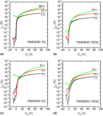
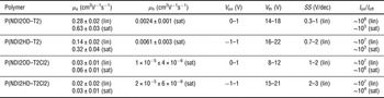
Representative n-channel operation transfer and output plots are shown in Fig. 5 and S4, whereas the OTFT device characteristics are summarized in Table II. The electron mobilities both in the linear and saturation regime of the parent non-chlorinated polymers (0.14–0.63 cm2V−1s−1) are found to be 5–10× larger than those of the corresponding chlorinated derivatives (0.02–0.05 cm2V−1s−1). The reduced electron mobilities most probably reflect backbone distorsions and the far greater band gap of the chlorinated semiconductors. V on (~0 V) and V th (~10–20 V) were found to be similar for all polymers. Significantly, the transfer characteristics of the representative optimized devices for all new semiconductors in the linear regime (V DS = 10 V) exhibit seven to eight order of magnitude current modulations, typical of high-performing organic polymer semiconductors.
Representative n-channel transfer curves for TG/BC OTFT devices of the indicated semiconductors.

Electrical parameters measured in ambient (RH ~ 40%) for TG/BC OTFTs (glass/thermally evaporated Cr–Au/semiconductor/PMMA/Au, L = 50 µm, W = 1000 µm) based on the indicated polymers. The results are given for the average of at least five devices.

Interestingly, the ambipolar characteristics of the chlorinated polymers are greatly suppressed (Fig. S5), resulting in hole mobilities of ~10–5 cm2V−1cm−1 in the saturation regime, which are about two orders of magnitude lower than those of the parent non-chlorinated systems (~10−3 cm2V−1cm−1). These results clearly reflect the stabilization of HOMO energies in the new polymers due to chlorination.
Device stability and OTFT operation in water
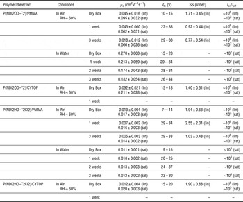
The present chlorinated NDI-based copolymers comprise a unique family of n-channel semiconductors exhibiting lowered LUMO energy levels (∆E LUMO = 0.1–0.2 eV) compared with the parent non-chlorinated systems and typical NDI-based copolymers. In general, the relative positions of the LUMO energies with respect to H2O- and O2-redox reactions determines the ambient stabilities of the electrons during the charge transport process in polymer thin films, and a LUMO energy level of <−4.0 eV combined with an hydrophobic gate insulator, is typically required for stable n-channel OTFT device operation.[ Reference Usta, Risko, Wang, Huang, Deliomeroglu, Zhukhovitskiy, Facchetti and Marks 79 , Reference Park, Lee, Lee, Lee, Lee, Yoon, Sung and Im 80 ] To this end, numerous small molecular n-channel semiconductors have been developed and exhibit good stabilities.[ Reference Usta, Kim, Wang, Lu, Huang, Facchetti and Marks 50 ] However, the number of n-channel polymers operating in ambient is still very limited and their operational stabilities are insufficient for most applications. More surprisingly, TFT operation under high-humidity and aqueous solutions has only been tested for a handful of polymers.[ Reference Hwang, Fuentes-Hernandez, Fenoll, Yun, Park, Shim, Knauer, Dindar, Kim, Kim, Kim, Cheun, Payne, Graham, lm, Anthony and Kippelen 81 ] Therefore, it remains very important to develop and understand the performance of new semiconductor materials with superior stabilities, including under the aforementioned extreme conditions, which will extend the scope of n-channel OTFTs in chemical and biological sensor applications in aqueous media.[ Reference Yun, Sharma, Fuentes-Hernandez, Hwang, Dindar, Singh, Choi and Kippelen 82 ] When compared with non-chlorinated NDI-based copolymers, the present copolymer semiconductors should exhibit better ambient stabilities. Thus, we investigated TG/BC transistor performance of the devices based on non-chlorinated P(NDI2OD–T2) versus those of the chlorinated P(NDI2HD–T2Cl2). The TFT structure for this study is glass/photolithography-Ni–Au/semiconductor/dielectric/Al, the gate dielectric is either PMMA (thickness ~500 nm, C i ~ 6.19 nF/cm2) or CYTOP (thickness ~ 380 nm, C i ~ 4.89 nF/cm2), and L = 20 µm/W = 1000 µm. The devices were first tested in a nitrogen filled glove box, and then stored under an average relative humidity of 60.5 ± 2.8% at 24.6 ± 1 °C for 1–3 weeks, during which time the devices were periodically measured.
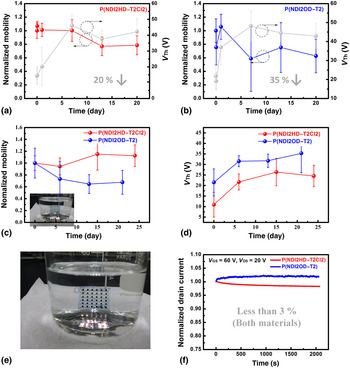
Figure S6 shows representative transfer plots whereas Figs. 6(a) and 6(b) report the mobility variations of these devices over time. Table III summarizes major TFT parameters for these devices. Although both P(NDI2HD–T2Cl2) and P(NDI2OD–T2) devices with PMMA as gate dielectric exhibit some degradation over time, overall P(NDI2HD–T2Cl2)-based devices showed better stabilities than P(NDI2OD–T2). Regardless of the lower electron mobilities of P(NDI2HD–T2Cl2) versus the well-studied P(NDI2OD–T2), P(NDI2HD–T2Cl2) devices exhibit a ~20% electron mobility degradation after ~1 week of storage, whereas higher degradation (35%) is recorded for P(NDI2OD–T2) (Fig. 6). Both devices exhibits a considerable V th shift from ~+(10–20) V to ~+(40–45) V after ~1 week of storage indicative of formation of deep traps. However, after these performance variations, the I–V characteristics stabilize and remain constant for the subsequent ~2 weeks. The TFT operation and improved stability of P(NDI2HD–T2Cl2)-based devices was further confirmed by submerging tests in water. As shown in Fig. S7, Fig. 6(c) and 6(d), the performance of P(NDI2HD–T2Cl2)-based OTFT devices with PMMA as the gate dielectric exhibit far lower degradation after 3 weeks submergence in water, whereas those based on P(NDI2OD–T2) exhibit larger degradation.
Device stabilities of P(NDI2HD–T2Cl2)-and P(NDI2OD–T2)-based OTFTs with PMMA in various conditions: ambient storage (RH: 60.5 ± 2.8 %,Temp.: 24.6 ± 1 °C) (a, b), H2O immersion (DI water) (c, d). (e) Optical image of a submerged device array. (f) Operational stability under supplied bias (V GS = 60 V, V DS = 20 V).

Electrical parameters of TG/BC OTFTs fabricates with P(NDI2OD–T2) and P(NDI2HD–T2Cl2) during stability measurements.

It is important to note that the devices fabricated with CYTOP dielectric are found to be highly unstable and quickly become unfunctional upon immersion in water. At first, this result appears to be quite surprising, because several groups reported excellent device stabilities for CYTOP devices in highly moisturized conditions as a result of the dielectric's high hydrophobic nature.[ Reference Yun, Sharma, Fuentes-Hernandez, Hwang, Dindar, Singh, Choi and Kippelen 82 – Reference Cheng, Caironi, Noh, Wang, Newman, Yan, Facchetti and Sirringhaus 84 ] It is likely that this behavior originates from the poor adhesion of CYTOP to both conjugated polymer films. In fact, the CYTOP/gate layer of the OTFTs immersed in water for one week was found to pill-off when the devices were blown with N2 gas to dry them before the electrical tests (Fig. S8). This result suggests that there could be penetration of ambient moisture into the solid films, which might cause delamination of the dielectric from the channel and result in the observed significant degradation.
Finally, bias-stress stability tests for the P(NDI2OD–T2)/PMMA and P(NDI2HD–T2Cl2)/PMMA devices were carried out in an N2-filled glove box to investigate the intrinsic stability of these devices when water/air is excluded. For this study, the TFT structure is glass/Au/semiconductor/dielectric/Al (W/L = 1000/20 µm). Under these conditions, both polymers exhibit excellent operational stabilities with <3% I on current variation [Fig. S9 and Fig. 6(f)].[ Reference Khim, Baeg, Kim, Kang, Lee, Chen, Facchetti, Kim and Noh 85 ] Overall, the improved stability in high-humidity/aqueous conditions for the devices based on P(NDI2HD–T2Cl2) indicate that chlorination is a facile modification strategy to broaden the application of NDI-based polymer semiconductors.
Conclusions
We have demonstrated the synthesis and characterization of new NDI-based chlorinated copolymers as novel n-channel semiconductors. Incorporation of chlorine substituents into the polymer π-backbone widens the band gap and lowers the frontier MO energy levels compared with their non-chlorinated parent polymers. The new chlorinated polymers exhibit suppressed ambipolarity and electron mobilities approaching 0.1 cm2V−1s−1 in a TG/BC OTFT architecture. The stability of the NDI polymer-based OTFTs was investigated both in high-humidity conditions and upon submersion in water. The enhanced environmental and operational stabilities, while keeping good transport characteristics, indicates that chlorination offers a facile new strategy to realize functional π-conjugated semiconducting polymers for chemical and biological sensor applications in aqueous media.
Supplementary material
For supplementary material for this article, please visit http://dx.doi.org/10.1557/mrc.2016.4
Acknowledgments
AF thanks KAU (grant no. 4-130-36-HiCi) for support. This work was supported by a National Research Foundation of Korea (NRF) grant, funded by the Korean Government (MSIP) (NRF-2014R1A2A2A01007159). GSR and YYN thanks to Paul S. K. Amegadze for helpful discussion.