Introduction
A directional filter (DF) is a completely matched four-port network which is a very useful component in a wireless communication system for separating and combining the channels. The ideal DF has the property that a wave incident to port 1 couples into port 3 with the response of a band pass filter while it does not couples into port 2 like band reject filter. Many DFs have been proposed and implemented using various kinds of waveguides and strip line technologies [Reference Cohn and Coale1–Reference Deslandes and Wu6]. The traveling-wave loop DF is very compact and any number of traveling wave resonators can be utilized to obtain increased off-channel rejection between the input port and coupled port. Substrate integrated waveguide (SIW) is considered attractive for the microwave and millimeter-wave components due to the high quality factor, compact size, low cost, and easy integration with planar circuits [Reference Danaeian, Moznebi, Afrooz and Hakimi7–Reference Song, Nura, Hu, Zhu, Chen and Fan11]. In addition, a half mode substrate integrated waveguide (HMSIW) is a newly proposed planar structure keeping the advantages of SIW with a reduction to nearly half in size [Reference Khorand and Bayati12–Reference Wang, You and Zhu14].
In [Reference Cheng, Hong and Wu13], a double loop HMSIW DF is proposed which involves three couplers at the center frequency of 12 GHz with 250 MHz bandwidth. The distance between HMSIWs in the loop is used to avoid their adjacent coupling and also inductive posts are used to help the wave travel in the loops fluently. An HMSIW DF with a complementary split ring resonator characterized by 5 dB fractional bandwidth (FBW) 6.2% at 19.7 GHz is presented [Reference Wang, You and Zhu14]. It is comprised two identical 3 dB directional couplers and two identical bandpass filters placed parallel between the 3 dB couplers leading to an increase in the circuit size. This paper presents a new DF based on SIW technology. It consists of two HMSIWs and two SICCs in cascade. The SICC resonators are designed to operate in the TM110 degenerate modes which exhibit directional properties, and each cavity through a continuous aperture is coupled to the adjacent cavity or HMSIW section. Two slotlines are introduced to adjust the coupling between two SICC resonators. The DF is one of the multiplexing to support a good filtering response. As well as the DFs are useful in communication systems and offer a good alternative to multi-channel systems for frequency division multiplexing a channel combiner or as a channel separator. A DF is a four-port device with a band pass response between two ports, and its reject-band between other ports.
Two-circular cavity SIW DF
Circular SIW cavity resonator
The basic dual-mode resonator in a circular SIW cavity is based on the utilization of two degenerate TM110 modes which are perpendicular to each other. The resonant frequencies of two degenerate TM110 modes in a circular cavity can be calculated by [Reference Pozar15].

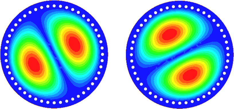
where c is the velocity of light in the vacuum, R is the equivalent radius of the SICC, μr and εr are relative permeability and permittivity of the substrate, respectively. Figure 1 shows the electric field distribution of the TM110-similar modes in a SICC using the full wave simulator Ansoft HFSS.
Electric field distributions of TM110 degenerate modes in a circular SIW cavity simulated by full wave simulation software Ansoft HFSS.

Directional filter design
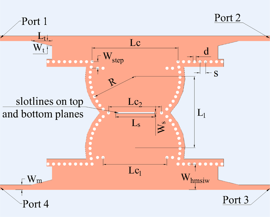
Figure 2 shows the layout of the proposed DF based on the SICC resonators, where port 1, 2, 3, and 4 are the input, through, coupled, and isolated port, respectively. At each port, the microstrip is connected with the HMSIW via a taper-shape transition [Reference Deslandes and Wu6]. The coupling structure between the HMSIW section and the circular SIW cavity consists of one continuous aperture, and a waveguide step is used to improve matching at the operating frequency band.
Layout of the proposed two-circular cavity SIW DF.

The design parameters for DF are specified in terms of the bandpass frequency response at the coupled port. This bandpass response is related to the coupling coefficients ki ,i+1 between the resonators, external quality factor Qe, and the response of a low-pass prototype filter. Hence, the element values of the low-pass prototype filter should be chosen first. Then, the design parameters are obtained by [Reference Matthaei, Young and Jones16]:


where w′ 1 is the cut-off frequency of the low pass filter, (Qe)A and (Qe)B are the external quality factors of the resonators at the input and output, respectively. λ′g is the wavelength of the guided wave and w 0 is the center frequency.


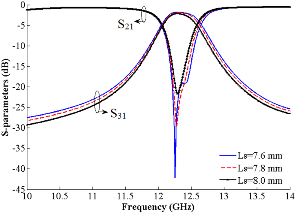
where (Ci ,i+1)2 is the power coupling factor, n is the number of half wavelengths in the resonators, and ω 1, ω 2 are the low and high cut-off frequencies. The quality factor is inversely proportional to BW. Then we should optimize the physical circuit to match the required coefficients and the dimensions of the DF can be determined. The proposed DF has three couplings of which two are identical, the bandwidth of the bandpass can be adjusted slowly. The maximally flat low-pass prototype parameters are g 0 = g 3 = 1 and g 1 = g 2 = 1.4142. Having obtained the low-pass parameters, we can obtain the design parameters for the SICC DF with the center frequency at f = 12.3 GHz and the bandwidth of BW = 400 MHz as follows: C 01 = C 23 = 0.94, and C 12 = 0.7934. As shown in Fig. 2, the proposed SICC DF is formed by two HMSIW sections and two SICC resonators. The coupling coefficient between two circular SIW cavities can be controlled by using two identical slotlines etched on the top and bottom planes. Figure 3 shows the simulated frequency response of the designed DF with different values of Ls. It can be seen that the bandwidth of the bandpass can be adjusted slowly by altering Ls. BW changed about 110 MHz for ΔL s = 0.4 mm. Finally, a fine-tuning procedure is often used to optimize the entire structure with Ansoft HFSS software. Power incident at port 1 emerges from port 3 and it looks like a band-pass filter and remaining power emerges port 2, looks like a band stop filter.
Simulated S-parameters of the proposed DF for different values of Ls.

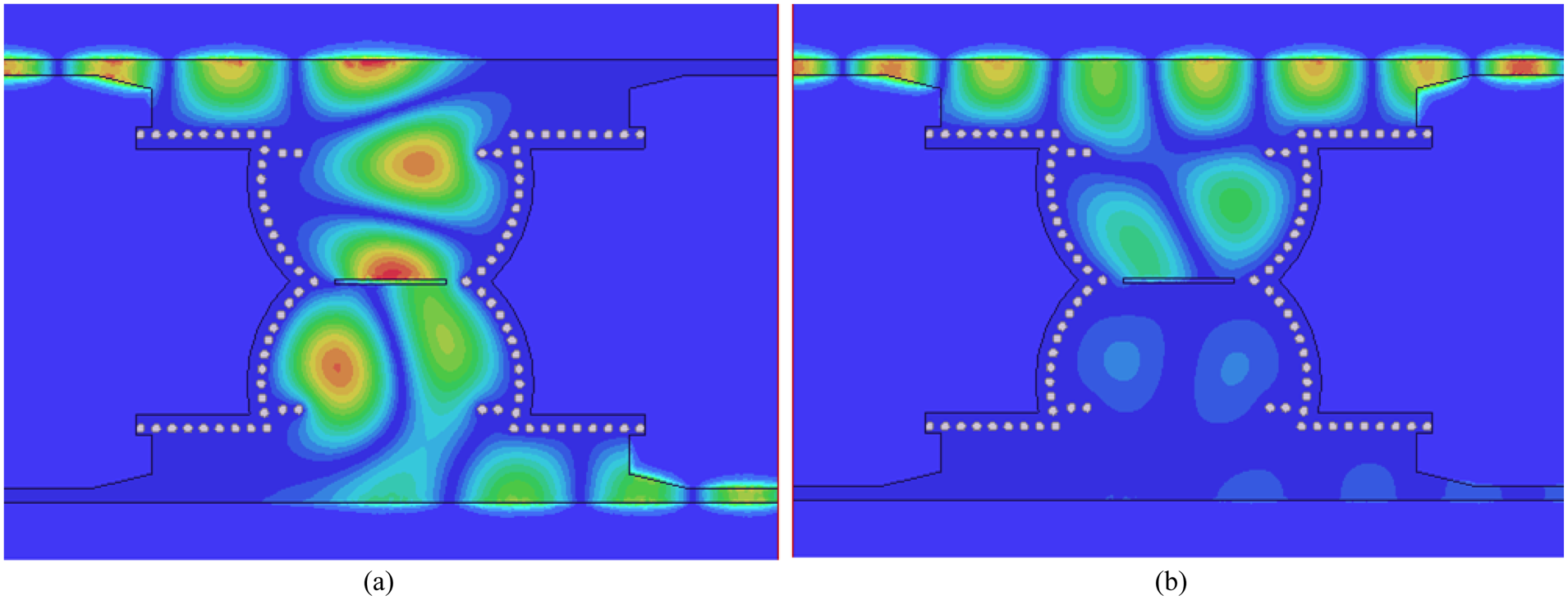
The E-field distributions of the optimized structure are shown in Fig. 4 at different frequencies. Figure 4(a) shows the distribution of E-field in the pass-band (at 12.3 GHz). According to Fig. 4(a), the input power at port 1 is transmitted to port 3. Figure 4(b) shows the distribution of the E-field out of band (at 13.3 GHz), that is given the input power at port 1 is not transmitted to port 3.
Electric field distribution for the (a) resonant frequency of SICC at 12.3 GHz and (b) far away from the resonant mode at 13.3 GHz.

Experimental results
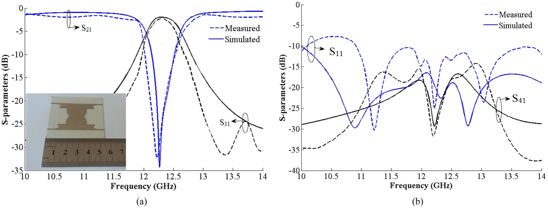
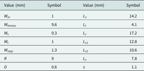
The proposed two-circular cavity SIW DF was fabricated over a Rogers RO4003 substrate with a relative dielectric constant of 3.38, thickness h = 0.508 mm, and loss tangent tan δ = 0.0027. The photograph of the fabricated DF is depicted in Fig. 5(a), and the optimized geometry parameters are summarized in Table 1. Simulated and measured results of the proposed DF are shown in Fig. 5. The measured return loss (S 11) and isolation between ports 1 and 4 (S 41) in the operating band are better than −10.5 and −15 dB, respectively. The minimum insertion loss is about 3.1 dB for S 31, and 1.4–1.6 dB for S 21 which are slightly lower than the simulated values, but the agreement are reasonable. The measured 3-dB passband ranges of S 31 from 12.05 to 12.45 GHz, or a bandwidth of 3.25% at the center frequency. Table 2 shows the comparison between the parameters of the proposed DF and other HMSIW DFs approached in the references, where it can be seen, the high miniaturization factor obtained with the proposed structure.
Measured and simulated S-parameters of the proposed DF.

Dimensions of the DF

Comparison with some prior DFs

The area of the proposed DF is 25% smaller than [Reference Cheng, Hong and Wu13] and the FBW of the proposed DF is 1.5 times larger than FBW [Reference Cheng, Hong and Wu13]. The higher discrepancies of results between simulation and measurement are due to the inclusion of the SubMiniature version A connectors and soldering in the measured circuit. On the other hand, substrate (tan δ), radiation, and pin losses can be affected.
Conclusions
A compact DF employing SICC resonators has been presented. Two slotlines are placed on the top and bottom planes to control the coupling between circular SIW resonators. In order to demonstrate the proposed scheme, a SICC DF has been designed, fabricated, and measured. The simulated results are in good agreement with the measured parameters. Compared with the conventional SIW DFs the proposed DF has a more compact size and simple structure.