I. INTRODUCTION
Mixed-phase TiO2 composites (anatase and rutile) have been shown to be more reactive than either pure phase alone because they have an advantageous combination of light-harvesting and charge-trapping abilities.Reference Li and Gray1–Reference Chen, Graham, Li and Gray4 Anatase/rutile interfaces are the critical feature of mixed-phase materials because they facilitate charge transfer and are the location of a unique population of electron trapping sites which may also behave as “catalytic hot spots.”Reference Li, Ciston, Saponjic, Chen, Dimitrijevic, Rajh and Gray3, Reference Hurum, Gray, Rajh and Thurnauer5, Reference Hurum, Agrios, Gray, Rajh and Thurnauer6 Direct current reactive magnetron sputtering (DCMS) has been utilized to synthesize mixed-phase TiO2 thin films with the objective of creating materials with high densities of anatase/rutile interfaces to take advantage of the charge transfer and trapping capabilities.Reference Chen, Graham, Li and Gray4, Reference Chen, Graham and Gray7, Reference DeSario, Chen, Graham and Gray8 Bulk mixed-phase proportionsReference Chen, Graham, Li and Gray4 and oxygen deficiencyReference Chen, Graham and Gray7, Reference DeSario, Chen, Graham and Gray8 in sputtered films have been optimized to enhance photoefficiency. Cation substitution (Nb) in titania has been investigated as a means to red-shift the photoresponse of the material into the visible light range by introducing defect energy levels in the host bandgap.Reference DeSario, Graham, Gelfand and Gray9, Reference Yang, Kim, Jha, Lee, Paul and Schmuki10 The objective of Nb doping in sputtered thin films is to create a visible light responsive material without deleteriously modifying the film’s photoactivity. Therefore, we must determine if the incorporation of Nb into thin films disrupts the interfacial structure of mixed-phase films. When cosputtering mixed-phase TiO2 with a dopant (Nb), it is unclear (i) how the two crystal phases are distributed within thin film structures, (ii) what the dominant interfaces are, and (iii) how the dopant is distributed within the crystal phases. In this study, we investigate by transmission electron microscopy (TEM) the distribution of dopants (Nb) and crystal phases (anatase and rutile) within mixed-phase Nb-doped TiO2 thin films (Ti1−xNbyO2) prepared by DCMS.
Most investigations of Nb substitution in TiO2 focus on the doping of a single phase,Reference Kurita, Ohta, Sugiura, Ohta and Koumoto11–Reference Ghicov, Yamamoto and Schmuki26 and no studies have investigated the relative solubility of Nb in mixed-phase materials. In our synthesis, dopants are added in a reactive sputtering process that produces mixed-phase films, but bulk characterization does not reveal if the dopant is homogeneously dispersed in the film or is segregated according to its solubility in anatase or rutile. We, and others, have observed that Nb substitution affects the bandgap and/or optical properties of anatase and rutile differently,Reference DeSario, Graham, Gelfand and Gray9, Reference Chambers, Gao, Kim, Henderson, Thevuthasan, Wen and Merkle27, Reference Das Mulmi, Sekiya, Kamiya, Kurita, Murakami and Kodaira28 therefore, it is important to know the dopant concentration within each phase. We have also observed preferred growth of rutile at high Nb concentrations, which suggests that Nb preferentially substitutes into rutile.Reference DeSario, Graham, Gelfand and Gray9 Also, dopants may segregate at grain boundaries, which generally accommodate defects. Since the interfaces are the location of “catalytic hot spots” and a unique population of electron trapping sites,Reference Li, Ciston, Saponjic, Chen, Dimitrijevic, Rajh and Gray3, Reference Hurum, Gray, Rajh and Thurnauer5, Reference Hurum, Agrios, Gray, Rajh and Thurnauer6 interfacially located Nb may alter the defect structure of the catalytically active interface.
As anatase/rutile interfaces are the key feature of highly active mixed-phase materials, it is important to characterize how Nb substitution affects the interfacial distribution of mixed-phase films. Nb changes the domains of crystal phase growth relative to undoped TiO2 (favoring rutile growth), and thus, different sputtering conditions must be utilized to prepare Ti1−xNbyO2 films with the same anatase:rutile ratio as TiO2 films.Reference DeSario, Graham, Gelfand and Gray9 We determine if mixed-phase Ti1−xNbyO2 films prepared under different sputtering conditions as mixed phase TiO2 films have the same interfacial structure of the undoped films. Undoped mixed-phase films contain a high density of anatase/rutile interfaces and ideally, a high density of these interfaces will also be formed when depositing Nb-doped mixed-phase films. Bulk characterization does not reveal if the interfacial structure of mixed-phase films is changed by the addition of a dopant. In this work, TEM is the nanoscale characterization method used to reveal the dispersion of crystal phases within film structures and characterize the interfaces. This characterization allows us to elucidate important structural details which are not revealed by bulk characterization techniques.
II. EXPERIMENTAL METHODS
DCMS with radio frequency (RF) bias was used to prepare Ti1−xNbyO2 thin films. This sputtering setup has been described in detail elsewhere.Reference Chen, Graham, Li and Gray4, Reference Sproul, Graham, Wong, Lopez, Li and Scholl29 Argon was used as the sputtering gas and oxygen was the reactive gas. A constant base pressure of 0.44 Pa was used and oxygen partial pressure was held constant at 0.12 Pa. This oxygen partial pressure was in the “oxide” sputtering regime and supplied excess oxygen to deposit fully stoichiometric/oxidized TiO2.Reference Chen, Graham and Gray7, Reference DeSario, Chen, Graham and Gray8 The films were deposited on Si wafer substrates at normal incidence. Target power and substrate RF bias were set at 3.5 kW (∼8.7 W/cm2) and −35 V, respectively, to produce mixed-phase films (anatase and rutile) at different phase proportions depending upon Nb concentration.Reference Chen, Graham, Li and Gray4, Reference DeSario, Graham, Gelfand and Gray9 Nb-doped thin films (Ti1−xNbyO2) were prepared through co-deposition of Ti and Nb by adding 0.25-inch-Nb slugs to a pure Ti sputtering target.Reference DeSario, Graham, Gelfand and Gray9 The concentration of Nb in the films was dependent upon the amount of dopant material added to the target and the position of the substrate relative to the position of the dopant in the target. A high Nb film and a low Nb film were prepared at 8.4 and 4.4 at.%, respectively, as determined by energy dispersive x-ray spectroscopy (EDX) using a Hitachi HD-2300 STEM (Evanston, IL, at 200 kV accelerating voltage). These Nb concentrations were chosen because they would yield mixed-phase films with different proportions of anatase and rutile. Plan-view TEM samples were prepared from the films by polishing, dimple grinding, and ion milling.
Scanning electron microscopy (SEM; Hitachi S4800-II, Evanston, IL, 10 keV accelerating voltage, 10-μA probe current) was utilized to observe the morphology of the films. X-ray powder diffraction (XRD) patterns were collected from bulk crystal by XRD (Rigaku, The Woodlands, TX) using Cu-Kα radiation operated at 40 kV–20 mA. The JADE software was used for peak fitting and quantification of mass ratios of anatase and rutile. The intensity of the anatase (101) and rutile (110) reflections (at 2θ = ∼25.5 and ∼27 degrees, respectively) was used in the Spur equation for quantification of mass ratios. Scherrer’s equation was used to determine average crystallite size from the full width at half maximum of the anatase (101) and rutile (110) reflections.
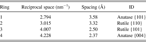
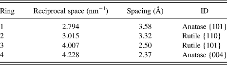
A JEOL HF-2100 STEM (Peabody, MA) operated in TEM mode (200 kV accelerating voltage) was utilized for dark-field imaging of anatase grains. An electron diffraction pattern was collected and indexed (Table I). The innermost diffracted ring, which has a spacing of 3.58 Å corresponding to anatase {101}, was used as the reflection (g) for central-beam dark-field imaging: the objective aperture was inserted and the beam was tilted so the aperture covered an area of the innermost diffracted ring. A series of dark-field images were collected in this manner by tilting the beam slightly so the aperture collected signal from different regions of the innermost diffracted ring. This was repeated until images had been collected from the full diameter of the anatase ring, and a total of 24 dark-field images were collected for one area of the film. A composite image was compiled by overlaying all 24 of the dark-field images showing all regions of anatase crystallinity in this area of the film. This same method could not be utilized to selectively image rutile because there was no position of the high contrast aperture where this aperture exclusively collected signal from a rutile ring.
Indexing of electron diffraction pattern for mixed-phase titania thin film.
EDX was utilized to measure average Nb concentrations in the films and also to determine concentrations in individual crystal phases.
A Hitachi HD-2300 STEM (200 kV accelerating voltage) was utilized to collect nanodiffraction patterns and EDX spectra from individual grains in the films to compare Nb concentration in anatase, rutile, and the bulk. For a particular grain, the nanodiffraction pattern was used to identify its crystal phase and the nano-EDX spectra were used to determine the concentration of Nb in the grain (a raw EDX spectrum is provided in the supplemental information). The entire process was repeated for the higher Nb film (∼8.4 at.%) and the lower Nb film (∼4.4 at.%). To confirm the EDX results, the JEOL STEM was used to compare bulk Nb concentrations with concentrations in anatase. The beam size was reduced to ∼1 nm and placed on grains identified as anatase in the dark-field images to collect EDX spectra for anatase. A larger beam size was utilized to collect bulk Nb concentrations.
III. RESULTS
A. Bulk characterization
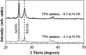
Figure 1 shows XRD patterns for the lower Nb (∼4.4 at.%) and higher Nb (∼8.4 at.%) Ti1−xNbyO2 thin films. Both films show the presence of the anatase and rutile reflections (at 2θ = ∼25.3 (101)A and 27.5 (110)R, respectively) with different proportions of each phase. The film with the higher Nb concentration exhibits a higher proportion of rutile (∼55% anatase and ∼45% rutile) compared to the film with a lower concentration of Nb (∼75% anatase and ∼25% rutile). Previous work from our group explored how sputtering parameters (i.e., target power, substrate bias, chamber pressure, etc.) control film growth and phase formation. The results showed that rutile formation was favored at high energy regimes, anatase formation was favored at low energy regimes, and mixed-phase films were prepared at intermediate energy regimes.Reference Li, Chen, Graham and Gray2, Reference Chen, Graham, Li and Gray4 When adding Nb to these films, it was observed that rutile growth is favored at higher Nb concentrations when all other sputtering conditions are the same.Reference DeSario, Graham, Gelfand and Gray9 From these diffraction patterns, the average anatase diameter is estimated to be ∼35–40 nm and the average rutile diameter is estimated to be ∼15–20 nm. The smaller diameter of rutile compared to the larger diameter of anatase is the reverse of what is observed in other synthesis. In most synthesis methods, rutile is formed when energy is added and anatase grains coarsen before converting into rutile. In reactive sputtering, rutile grains are nucleated as the film is grown, and thus, do not pass through anatase crystallinity before converting to rutile. Also, under energy regimes which favor anatase formation, the anatase phase displays more growth so it grows larger than rutile, which shows less growth. For these reasons, rutile grains are smaller on average than anatase grains.
X-ray diffraction plots for Ti1−xNbyO2 thin films prepared at 3.5 kW and −35 V bias with 4.4 and 8.4 at.% Nb. A—anatase (101). R—rutile (110).

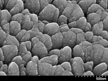
Figure 2 is a plan-view SEM image of the 4.4 at.% Nb film. This image shows the characteristic “bundled columnar structure” of the sputtered films.Reference Chen, Graham, Li, Gentner, Dimitrijevic and Gray30 Two distinct types of features are observed: (i) there are smaller columnar structures on the order of 30–80 nm in diameter grown from the substrate in the direction of flux from the target, and (ii) the columns are bundled together in larger features, which are on the order of several hundred nanometers in diameter.
Plan-view scanning electron microscopy image of mixed-phase (∼75% anatase and ∼25% rutile) sputtered TiO2 thin film.

Two types of interfaces are also observed in the SEM image. There are interfaces between the larger bundled structures and there are also interfaces within these structures between the smaller columns. While the SEM image reveals a high density of interfaces and the XRD pattern reveals that this film is mixed phase, the bulk characterization does not reveal if the column bundles contain both phases, how the phases are dispersed within the bundles, and if the dominant interfaces are anatase/rutile interfaces.
B. Rutile/anatase phase mapping
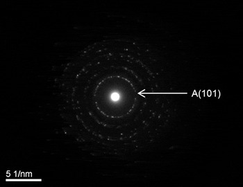
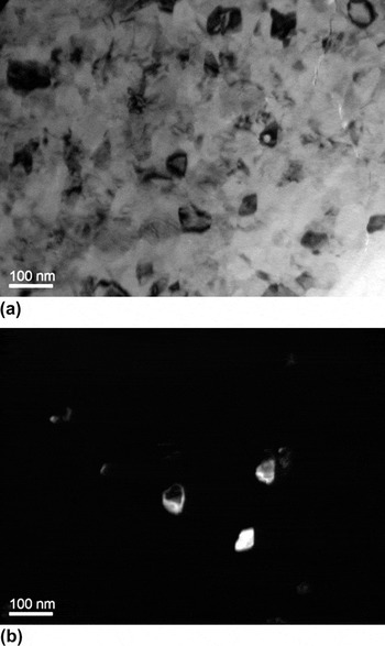
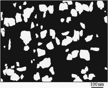
Figure 3 shows an electron diffraction pattern collected from the 8.4 at.% Nb film. The diffracted rings were indexed (Table I). Similar to the XRD pattern (Fig. 1), the electron diffraction pattern shows reflections of both the anatase and rutile phases. The innermost diffracted ring has a spacing of 3.58 Å, which corresponds to anatase {101}. This ring is used for dark-field imaging of anatase. Figure 4(a) is a bright-field image collected from the same area as the electron diffraction pattern in Fig. 3. Figure 4(b) is a dark-field image collected from this area with the aperture in place to collect signal from a portion of the innermost diffracted ring. The bright-field image shows crystallites at the same relative size as the particle size diameter predicted by Scherrer’s equation from the XRD pattern. Several larger grains on the order of 35–40 nm and several smaller grains on the order of 10–15 nm are observed. The anatase grains identified in the dark-field image are highlighted in the bright-field image. The size of these anatase grains in the dark-field image are also in good agreement with the average diameter determined by XRD. Twenty-four dark-field images similar to Fig. 4(b) were collected from different areas on the innermost diffracted anatase ring to cover the entire diameter of the ring. These images were compiled into one image, as shown in Fig. 5.
Electron diffraction pattern collected from mixed-phase titania thin film. The pattern shows anatase and rutile diffracted rings. The inner most ring has a spacing of 3.58 Å which corresponds to anatase (101).

(a) Bright-field and (b) dark-field images collected with the high contrast aperture on diffracted anatase ring. The bright grains on the dark-field image (b) are anatase and these grains are outlined in the bright-field image (a).

Compilation of dark-field images collected with aperture on innermost diffracted ring (anatase). The white regions of this image are anatase grains that diffracted to the anatase (101) ring. The black regions are rutile, amorphous, or anatase grains that did not diffract to anatase (101).

In the compiled dark-field image, the white areas represent regions of anatase grains. From this image, it is evident that the domains of anatase crystallinity are generally on the order of 10–100 nm. The largest anatase clusters are on the order of two to three grains, according to the average diameter estimated from the XRD patterns, indicating that the anatase crystallites are homogenously dispersed throughout the film. The total area comprised of anatase is in good agreement with the anatase fraction calculated from the XRD pattern. This image can also be compared to the SEM image (Fig. 2) to compare the domains of crystallinity with the size of the various features observed by SEM.
C. Distribution of Nb
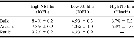
The EDX results are summarized in Table II. Using the Hitachi STEM, Nb concentrations were measured for grains whose phase was identified from nanodiffraction patterns. We collected EDX spectra from a total of four grains (two anatase and two rutile) for the high Nb film and from a total of ten grains (five anatase and five rutile) for the low Nb film. Table II summarizes Nb concentrations measured in anatase grains, rutile grains, and in the bulk for the high Nb and low Nb film. In the higher Nb film, the bulk concentration is 8.4 at.%, while concentrations in anatase are lower (7.3 at.%), and concentrations in rutile are enriched (9.2 at.%) compared to the bulk. In contrast, in the lower Nb film, the bulk concentration is 4.5 at.% and the concentrations in anatase (4.3 at.%) and rutile (4.4 at.%) are approximately the same.
At.% Nb measured in anatase grains, rutile grains, and in the bulk for high and low Nb films.
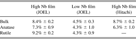
To confirm Nb segregation at higher concentrations, EDX measurements were also recorded for the high Nb film using the JOEL STEM. The results confirm that for this film Nb concentrations in anatase grains (6.3 at.%) are significantly lower than in the bulk (8.7 at.%).
IV. DISCUSSION
A. Distribution of crystal phases
Sputtered mixed-phase films are synthesized with the objective of creating a high density of anatase/rutile interfaces, which facilitate charge transfer and trapping and are the location of catalytic “hot spots.”Reference Li, Ciston, Saponjic, Chen, Dimitrijevic, Rajh and Gray3, Reference Hurum, Gray, Rajh and Thurnauer5, Reference Hurum, Agrios, Gray, Rajh and Thurnauer6 We previously demonstrated that using DCMS mixed-phase materials with a high density of anatase/rutile interfaces could be synthesized and bulk mixed-phase proportions can be tuned to optimize photocatalytic activity.Reference Chen, Graham, Li and Gray4 Nb substitution in sputtered mixed-phase films (Ti1−xNbyO2) was studied to enhance visible light harvesting of these mixed-phase composites.Reference DeSario, Graham, Gelfand and Gray9 Ideally, Nb can be incorporated into these structures to some level to enhance light absorption without disrupting the anatase/rutile interfacial density. In this work, we determine how the anatase and rutile phases are distributed in Ti1−xNbyO2 mixed-phase films to determine if high densities of anatase/rutile interfaces are maintained in these films.
Although the SEM image reveals a high density of interfaces and the XRD pattern shows that this film is mixed phase, the bulk characterization cannot determine how the phases are dispersed within Ti1−xNbyO2 films. The composite dark-field image shows that the domains of anatase crystallinity are on the order of 10–100 nm and indicates that the anatase grains are homogenously dispersed in the Ti1−xNbyO2 mixed-phase film. The domains of anatase crystallinity illustrated in Fig. 5 can be compared to the size of the features observed in the SEM image in Fig. 2. From this comparison, we conclude that at this bulk anatase:rutile ratio the larger features in the SEM image (the “column bundles”) are comprised of both anatase and rutile and the columns within the larger bundles are different phases. Since these larger features are mixed phase, we can conclude that the interfaces within these features, which are the dominant interfaces observed in the films, are likely to be anatase/rutile interfaces.
Nb substitution changes the phase proportions relative to undoped films, and therefore, different sputtering conditions must be utilized to prepare Ti1−xNbyO2 films with the same anatase:rutile ratio as TiO2 films. Even at the higher concentrations (∼8.4 at.%), Nb substitution does not disrupt the homogeneous dispersion of the anatase and rutile phase in mixed-phase films and the high density of anatase/rutile interfaces are preserved.
B. Distribution of Nb
Although Nb substitution in TiO2 has been studied extensively, these studies generally focus on substitution into a single phase,Reference Kurita, Ohta, Sugiura, Ohta and Koumoto11–Reference Valigi, Cordischi, Minelli, Natale, Porta and Keijzers25 and mixed-phase systems have not been studied. In our synthesis process, Ti and Nb are cosputtered while the anatase and rutile phase are simultaneously deposited. In this sputtering process, it is unclear if the dopant will be homogeneously dispersed in the film or if it will segregate in a particular phase. Nb substitution affects the bandgap structure and optical properties of anatase and rutile differently,Reference DeSario, Graham, Gelfand and Gray9, Reference Chambers, Gao, Kim, Henderson, Thevuthasan, Wen and Merkle27, Reference Das Mulmi, Sekiya, Kamiya, Kurita, Murakami and Kodaira28 therefore, it is important to know the dopant concentration within each phase.
This study reveals that the dispersion of Nb in the films is found to be concentration dependent. At lower bulk Nb concentrations (∼4.4 at.%), Nb is homogenously dispersed in the films and the concentration in anatase, rutile, and the bulk are nearly equal. At higher bulk Nb concentrations (∼8.4 at.%), Nb concentrations are higher in rutile and lower in anatase compared to the bulk. At these higher concentrations, the XRD patterns also show a higher proportion of rutile. As Nb concentrations increase, the films transition to pure rutile and eventually are amorphous.Reference DeSario, Graham, Gelfand and Gray9
These results suggest that when cosputtering Ti and a dopant cation into mixed-phase materials, the dopant cation may segregate preferentially in a given phase. There is an apparent concentration threshold above which Nb is found to preferentially substitute into rutile. This may be explained by the higher solubility of Nb in rutile as NbO2 forms a rutile-like structure.Reference Chambers, Gao, Thevuthasan, Liang, Shivaparan and Smith24, Reference Sakata31, Reference Marinder and Magneli32 The high solubility of Nb in rutile has been previously demonstrated in several studiesReference Furubayashi, Hitosugi, Yamamoto, Inaba, Kinoda, Hirose, Shimada and Hasegawa12, Reference Morris, Dou, Rebane, Mitchell, Egdell, Law, Vittadini and Casarin18, Reference Gao, Liang and Chambers23, Reference Chambers, Gao, Thevuthasan, Liang, Shivaparan and Smith24, Reference Chambers, Gao, Kim, Henderson, Thevuthasan, Wen and Merkle27, Reference Marinder and Magneli32, Reference Antonio, Song and Yamada33 and at least one study has shown that there is no solubility limit for Nb in the TiO2 lattice.Reference Antonio, Song and Yamada33 There are also reports that Nb substitution promotes the transition of anatase to rutile,Reference Depero, Sangaletti, Allieri, Bontempi, Salari, Zocchi, Casale and Notaro17 consistent with our observations with sputtered films.Reference DeSario, Graham, Gelfand and Gray9 The preferential segregation of Nb in rutile may be one factor which promotes the growth of rutile in sputtered mixed-phase films.
In other morphologies of TiO2, Nb can be incorporated into anatase without promoting rutile.Reference Ghicov, Yamamoto and Schmuki26, Reference Zhang, Ikeda, Uchikoshi, Li, Watanabe and Ishigaki34 Ghicov et al.Reference Ghicov, Yamamoto and Schmuki26 have synthesized TiO2 nanotube arrays with 33.33 at.% Nb that did not show any rutile. In the case of nanotube arrays, the geometrical limits imposed by nanotube walls prevent rutile nucleation and crystallites cannot obtain the proper orientation to transition to rutile.Reference Zhang and Banfield35–Reference Aldabergenova, Ghicov, Albu, Macak and Schmuki37
The results of this study show that bulk measurements of dopant concentration are not necessarily accurate at the nanoscale and tend to only reflect average characterization. When cosputtering a dopant cation in a reactive sputtering process, the dopant may not be homogeneously dispersed in the film and may segregate according to phase solubility.
V. CONCLUSIONS
This work employs TEM to probe the composition and structure at the nanoscale and elucidates important structural details in Nb-doped mixed-phase titania films that are not revealed by bulk characterization techniques. Dark-field TEM imaging, electron diffraction, and EDX were utilized to determine the dispersion of anatase grains, rutile grains, and Nb dopants in mixed-phase TiO2 thin films prepared by DCMS. This study revealed that anatase and rutile phases are homogenously dispersed in Ti1−xNbyO2 films, indicating a high density of anatase/rutile interfaces. The anatase/rutile interface is a critical feature of mixed-phase films that accounts, in part, for their high reactivity. At low Nb concentration, Nb was found to be homogeneously dispersed in the films, while at high concentrations, Nb concentrations were higher in rutile and lower in anatase. The results indicate that there is a concentration threshold beyond which Nb segregates according to its higher solubility in rutile. The segregation of Nb into rutile may be one factor which promotes the formation of rutile in mixed-phase films. The results of this study also show that bulk measurements of dopant concentration may not be accurate in mixed-phase materials at the nanoscale.
ACKNOWLEDGMENTS
The financial support provided for this study from the NSF Grant no. CBET-0829146 is gratefully acknowledged. The characterization (XRD, TEM, and SEM) was performed in the JB Cohen x-ray facility and the NUANCE research centers at Northwestern University. We also thank Matthew K. Waltz for his assistance with image processing.