Introduction
Despite the fact that photons have no mass, light applies a force on objects on which it shines. The physics involved is very similar to what happens when a billiard ball is sent into a well-defined direction upon the impact of another ball. In the same way, a photon impinging on an object transfers its momentum, resulting in a force known as radiation pressure. Radiation pressure from sunlight is known to affect the shape of a comet’s tail when orbiting around the sun. Back in the 1980s, Ashkin proposed and demonstrated the use of optical forces at a focused laser beam to trap and manipulate in 3D small objects in solution.Reference Ashkin, Dziedzic, Bjorkholm and Chu1 This seminal work initiated the active field of optical tweezers (OT) (also known as optical manipulation). Extensive research over the last 30 years has contributed to increase the level of control of OT, transforming them into a flexible and non-invasive tool capable of making objects spinReference Paterson, MacDonald, Arlt, Sibbett, Bryant and Dholakia2 or sorting them based on their differences in size or material.Reference MacDonald, Spalding and Dholakia3 Furthermore, this optical tool has strongly benefited the field of biology by enabling non-invasive manipulation of individual living cellsReference Ashkin, Dziedzic and Yamane4 and pushing the understanding of molecular motors by probing their mechanical response and dynamics.Reference Bustamante, Bryant and Smith5
While conventional OT can be applied to micrometer-sized specimens, trapping of smaller sizes is challenging. Indeed, reducing the size of the object has two main effects, both working against stable trapping. First, the magnitude of the trapping forces (gradient forces) decreases rapidly (following an R 3 law, where R is the radius of the trapped specimen), resulting in a shallower trap. Second, the damping of the trapped specimen decreases due to the reduction of the viscous drag that is responsible for an increase of Brownian motion. Both effects alter the confinement of the specimen within the trap. For a fixed average thermal energy k BT (k B being the Boltzmann constant and T the absolute temperature in the trap), this increasing delocalization is responsible for specimen escape from the trap.
To compensate for these effects and achieve trapping of smaller objects, one can either (1) increase the trap confinement by further focusing the trapping laser light, and/or (2) augment the depth of the trapping potential by increasing the local field intensity. Extending optical trapping down to the nanometer scale would open unprecedented opportunities in many fields of science in which these nano-OT would provide ultra-accurate positioning and manipulation of single nano-objects. In practice though, the minimum size for a laser focus is imposed by diffraction and limited to a relatively large fraction of the incident wavelength. As an alternative, several theoretical studies in the 1990s suggested exploiting the latest advances in nano-optics to extend OT to the nanometer scale.Reference Girard, Dereux and Martin6–Reference Okamoto and Kawata9 Indeed, unlike propagating fields, evanescent fields can be concentrated well beyond the diffraction limit. The interaction of the propagating incident laser with the nanostructure leads to the creation of large wave vectors k associated with evanescent waves, responsible for a subwavelength (sub-λ) concentration of light fields. In other words, the illuminated nanostructure acts as a nanolens capable of concentrating light well beyond what allows the high numerical aperture objective lens of a microscope. Among different branches of nano-optics, plasmonics that exploits surface plasmon resonances supported by metallic nanostructures is particularly powerful to concentrate propagating light into nanoscale volumes with enhanced intensity. By simultaneously addressing requirements (1) and (2), plasmonics opens new opportunities for optical manipulation of nano-objects that could contribute to the development of future optical and electronic nanodevices and integrated bioanalytical platforms.
Enhanced optical forces at a flat metallic film
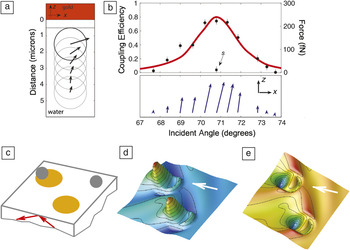
Let us first consider the simple case of surface plasmon polaritons (SPPs) sustained at a flat metal/dielectric interface. SPPs are surface waves associated with a resonant collective oscillation of the free electrons of the metal driven by a p-polarized optical field. They lead to surface fields decaying exponentially on both sides of the interface, whose magnitude is dramatically enhanced with respect to the incident fields. As a direct consequence of their evanescent nature, coupling to SPPs cannot be directly achieved with light propagating in free space but requires compensating momentum mismatch between incident photons and SPPs. In the most popular coupling method, the so-called Kretschmann–Raether configuration, this is done by illuminating a thin metal layer under total reflection through a glass prism. SPP fields have been extensively used to enhance different kinds of low efficiency physical processes. Song et al. suggested that SPPs could benefit optical manipulation by enhancing the magnitude of optical forces and thus reducing the power requirements of conventional OT.Reference Song, Han and Chang10 A few years later, Volpe et al. used photonic force microscopy to experimentally probe the enhanced force field induced by an SPP.Reference Volpe, Quidant, Badenes and Petrov11 Their data, displayed in Figure 1a, show the evolution of the force vector with distance to the surface. Owing to the exponential field decay, its magnitude increases exponentially when approaching the metal. In Figure 1b, the force vector evolution with the incident angle is shown for a fixed distance to the surface. Under p-polarization, the total force modulus closely follows the dispersion of the SPP featuring a clear resonance at the SPP angle. The enhancement factor associated with the SPP resonance was found to be as high as 40.Reference Volpe, Quidant, Badenes and Petrov11
(a–b) Enhanced surface plasmon polariton (SPP) force field at a homogeneous gold/water interface: (a) Evolution of the SPP force vector as a function of the bead-metal surface distance. (b) Evolution with the incident angle θ and polarization of the SPP force vector for a fixed distance to the surface of 500 nm. (c–e) Illustration of SP trapping on a patterned metallic surface: Two gold disks lying on a plane transparent surface are illuminated by total internal reflection (θ = 70°, p-polarization). (c) Geometry of the system where gray spheres are 20-nm-radius polystyrene beads; (d) calculated electrical intensity map computed 10 nm above the gold pad; and (e) associated optical potential trap experienced by a 20-nm-radius polystyrene particle. In (d) and (e), the white arrow points along the incident in-plane wave vector, and image sizes are 1100 nm × 1100 nm. Color scale indicates increasing values of both the field intensity and optical potential when going from blue to red. s-polarized.

At about the same time, Garcés-Chávez and co-workers reported on the use of plasmonic forces at a flat gold/water interface to self-assemble a large number of micrometer-sized dielectric beadsReference Garcés-Chávez, Quidant, Reece, Badenes, Torner and Dholakia12 with a single low intensity laser beam. Also, this work raised for the first time the question of the actual contribution of photothermal effects in the use of SPP for trapping. Coupling light to the SPP resonance is indeed associated with a significant increase of the metal temperature and subsequent heat release into the surrounding solution, responsible for thermally induced fluid dynamics such as convection and thermophoresis. It was shown that minimizing the height of the chamber enables a drastic decrease of thermally induced effects with respect to purely optical ones. More recently, Wang et al. made use of enhanced SPP forces at a flat gold/water interface to efficiently propel/guide small metallic nanoparticles in the surface plane.Reference Wang, Schronbrun and Crozier13
Plasmonic trapping at a (micro-) patterned metallic film
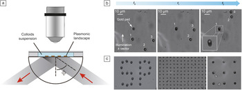
Because SPPs at a flat metallic film lead to a homogeneous optical force field, trapping at a predefined location of the surface requires patterning the metal to introduce a lateral confinement of the trapping well (Figure 1c–e). The first experimental implementation of SP trapping was demonstrated using a glass surface decorated by micrometer-sized gold disks.Reference Righini, Zelenina, Girard and Quidant14 In this experiment, the patterned surface is illuminated though a glass prism (Kretschmann configuration) by an unfocused (≈100 μm waist), linearly p-polarized near-infrared laser beam (Figure 2a). The gold pattern is covered by a static fluidic chamber containing a diluted aqueous suspension of micrometer polystyrene (PS) beads. At an angle of incidence matching the SPP resonance angle, light efficiently couples to the SPP mode supported by the top gold/water interface, and due to the combined effect of the boundaries and the asymmetrical illumination, leads to a concentrated plasmonic field in the forward portion of the disk. Figure 2b shows trapping of a bead in a forward portion of the pad where the maximum of the SPP field intensity is localized. Trapping times of up to several hours are achieved for an incident laser intensity of 107 W.m–2, which is about two orders of magnitude smaller than what is required in conventional OT for the same bead size.
Experimental surface plasmon (SP)-based trapping at a micro-patterned gold film: (a) Schematic of the experimental setup, in which a pattern of micrometer-sized gold disks is illuminated under the Kretschmann configuration through a glass prism. (b) Frame sequence illustrating the trapping of a 4.8 μm polystyrene bead in the forward position of a gold disk (t 0, t 1, and t 2 are successive times, and 1, 2, and 3 point to three different beads). The vertical white arrow gives the direction of the incident in-plane wave vector. The inset at time t 2 shows a trapped bead in the forward region of the gold pad at higher magnification. (c) Parallel trapping of polystyrene beads (black) and yeast cells (gray) using a single laser beam.Reference Juan, Righini and Quidant43 Φ, incident angle.

As mentioned previously, when the pad is much smaller than the illumination spot, the experiment can be extended to an ensemble of trapping sites to achieve, upon the same illumination conditions, parallel trapping of a large number of beads (Figure 2c). Parallel SP trapping opens new possibilities in the manipulation of micrometer-sized objects with potential application to different fields, including self-assembly and biology. In the context of cell biology, for instance, SP traps provide an efficient and compact approach to immobilize individual living cells or bacteria and inspect them optically.Reference Huang, Maerkl and Martin15
Interestingly, SP trapping can be combined with conventional integrated optics in order to achieve further integration by avoiding the use of bulk optical elements such as objective lenses and glass prisms. In the study in Reference 16, SP traps were implemented on top of a channel waveguide formed by ion implantation whose dispersion was engineered to match the dispersion of the SPP supported by each of the gold pads. It was shown that end-fire coupling to the waveguide using an optical fiber leads to similar trapping efficiency as compared to prism coupling.
As mentioned earlier, optical forces may coexist with some thermally induced forces. Although there is no clear data so far to quantify the respective contribution of optical and thermal effects, very recent hydrodynamics calculations indicate that the heat-induced fluid velocity near the structure would be negligible under the typical intensities used in SP tweezer experiments.Reference Donner, Baffou, McCloskey and Quidant17
Trapping with optical antennas
Beyond isolated metallic microstructures supporting SPPs, trapping of submicrometer objects can be achieved by exploiting the latest advances of plasmonics. Of particular interest is the gap antenna geometry, also known as plasmonic dimers, in which strong field intensity concentration is achieved in the nanometer gap between two adjacent metallic nanoparticles. Due to their huge potential for enhancing light-matter interaction at the nanoscale, gap antennas have lately raised expectations in different fields ranging from spectroscopyReference Zhu, Banaee, Wang, Chu and Crozier18 and sensingReference Aćimović, Kreuzer, González and Quidant19 to nonlinear optics.Reference Harutyunyan, Volpe, Quidant and Novotny20
In the context of optical trapping, their ability to concentrate laser light into strongly localized and intense hot spots makes gap antennas particularly attractive to create optical traps that can be orders of magnitude smaller than what can be achieved with the original pad approach,Reference Righini, Zelenina, Girard and Quidant14 thus enabling the extension of SP-trapping to the nanometer scale. Numerical calculations by Xu et al. first predicted that hot spots in the gap of metallic dimers could increase the residence time of single molecules in surface-enhanced Raman spectroscopy experiments.Reference Xu and Käll21
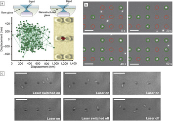
Grigorenko et al. proposed using gap antennas to assist conventional OT.Reference Grigorenko, Roberts, Dickinson and Zhang22 In their experiment, a 200 nm PS bead, trapped in a viscous medium at the tight focus of a 1064 nm laser beam, was brought in close proximity to a surface patterned with pairs of gold cylinders designed to be resonant at the same wavelength. As illustrated in Figure 3a, the antenna hot spot modifies the overall optical potential experienced by the bead, leading to a reduction of the trapping volume beyond the diffraction limit; this trapping volume is responsible for a one order of magnitude increase of the bead confinement.
Antenna trapping. (a) Gap antennas formed by two adjacent gold nanoparticles can assist conventional optical tweezers to reduce the spatial confinement of 200 nm polystyrene beads down to subwavelength dimensions.Reference Grigorenko, Roberts, Dickinson and Zhang22 The red spot on the micrograph indicates the spread of the trapped bead positions. (b) An array of gold gap antennas illuminated by an unfocused laser beam enables the parallel trapping of a large number of 200 nm polystyrene beads.Reference Righini, Ghenuche, Cherukulappurath, Myroshnychenko, García de Abajo and Quidant23 Note all circles (green and red) locate an antenna. With time, the green circles indicate the antennas that have trapped a polystyrene bead. (c) This later configuration also applies to parallel trapping of Escherichia coli bacteria and makes it possible to align them along the long antenna axis.Reference Righini, Ghenuche, Cherukulappurath, Myroshnychenko, García de Abajo and Quidant23

Shortly after, optical antennas were used as autonomous nano-optical traps, operated without the use of an auxiliary conventional OT. An array of gap antennas, each formed by two identical 500 nm gold bars, provided a platform to trap in parallel, upon unfocused illumination, a large number of individual 200 nm PS beads at the antennas gapsReference Righini, Ghenuche, Cherukulappurath, Myroshnychenko, García de Abajo and Quidant23 (see Figure 3b). The latter configuration also applies to biological samples such as living Escherichia coli bacteria. Interestingly, in addition to being efficiently trapped, the bacteria systematically aligned along the long axis of the antenna (see Figure 3c). This effect is attributed to the multipolar mode of the antennas that leads to secondary hot spots at the outer extremities. The elongated shape of the bacteria enables it to exploit the several trapping sites along the overall antenna until stabilizing into a minimum-energy equilibrium position.
More recently, several studies have further advanced the use of gap antennas for trapping. Tsuboi et al. demonstrated trapping of single quantum dots in the gap of gold dimers fabricated by angle-resolved nanosphere lithography.Reference Tsuboi, Shoji, Kitamura, Takase, Murakoshi, Mizumoto and Ishihara24 Zhang et al. achieved trapping of gold nanoparticles as small as 10 nm in the gap of dipolar gold gap antennas.Reference Zhang, Huang, Santschi and Martin25 While both types of objects can be trapped with conventional OT due to their high refractive index (which makes them behave like substantially bigger dielectric nanoparticles), the antenna makes it possible to trap them under much lower incident laser intensities.
Extending SP trapping to the nanometer scale using self-reconfigurable traps
Plasmonic nanostructures offer strong field gradients and large local intensities that allow one to engineer smaller and stiffer optical traps. However, previously discussed configurations suffer from a practical limitation that prevents decreasing the size of the trapped specimen beyond a certain size. Indeed, one unavoidably reaches a limit above which the required local intensity within the trap damages the trapped specimen and/or the metallic structure due to photoheating.Reference Ashkin, Dziedzic, Bjorkholm and Chu1 Even when not reaching such extreme limits, thermal effects can play an increasing role in the object’s dynamics and, in some cases, dominate optical forces.
Further extending optical trapping toward the nanometer regime thus requires additional refinements in the trapping mechanism. The usual approach to optical trapping, as considered previously, relies on a static picture in which the potential well is optimized for a given object and remains constant over the experiment: no modifications over time are applied to this potential well to account for the stochastic aspect of Brownian motion. While the average kinetic energy of the object within the trap is given by k BT, its instantaneous velocity follows a Maxwell-Boltzmann distribution in which the object energy can occasionally largely exceed the average value. Potential depths of about 10 k BT are typically used to compensate for these high-energy events. A depth of k BT would only hold the object until a high-energy event occurs.
Conversely, a dynamical approach in which the trapping potential is dynamically reconfigured to compensate for high-energy events would enable strong reduction of the required average trap depth. With this aim, external real-time feedback techniques have been implemented on conventional OT to correct the trapping potential by adjusting either the laser intensityReference Ashkin and Dziedzic26 or the trap position.Reference Simmons, Finer, Chu and Spudich27 In practice, the external feedback increases the effective stiffness of the trap,Reference Wallin, Ojala, Hæggström and Tuma28 enabling further confinement of the object by adding an external source of damping.Reference Ashkin and Dziedzic26 Although this approach relaxes the requirements on the local intensity within the trap, reducing the likelihood of optical damage,Reference Wallin, Ojala, Hæggström and Tuma28 it relies on a complex auxiliary feedback setup and is challenging to apply to very small specimens.
Alternatively, one can exploit the extreme sensitivity of plasmonic nanostructures to their dielectric environment to achieve some control of the SP-trap features. The dependence of plasmon resonances on tiny changes in the surrounding refractive index has been extensively exploited to design efficient and compact sensors for gas/liquid and biomolecule detection.Reference Willets and Van Duyne29 In the context of optical trapping, this sensitivity can have a destructive impact whenever the presence of the trapped object in the trapping site reduces the field gradient and/or local intensity, as reported in Reference 30. Conversely, plasmonic structures can also be devised such that the trapped object induces a constructive effect that favors trapping. Along this line, García de Abajo and co-workers theoretically proposed exploiting the sensing ability of plasmonic nanostructures to achieve a reconfigurable nanotrap.Reference Sainidou and García de Abajo31 In this configuration, a gold nanorod is trapped in the strong local field of a microvoid drilled in a gold film. As the distribution and spectrum of the microvoid mode strongly depends on the nanorod position, the latter can be tuned by changing the illumination wavelength.
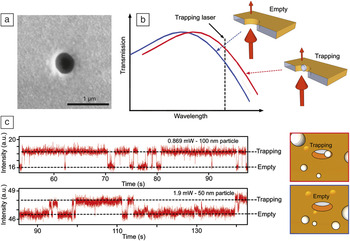
A step further consists of fully exploiting the trap/specimen interaction to achieve automatic feedback control that does not require any external monitoring/correcting procedure. For this, one first aims at optimizing the trapping efficiency by properly engineering the plasmonic mode, such that the local intensity within the trap is maximized in the presence of the object. As a consequence, the momentum of the (plasmonic) photons interacting with the object experiences significant changes as the object moves in and out of the trap. Due to momentum conservation, these changes create an additional dynamical force field that is in essence automatically synchronized with the object’s dynamics. The first demonstration of the so-called self-induced back-action (SIBA) has recently been performed using a nanoaperture in a metallic film (Figure 4a).Reference Juan, Gordon, Pang, Eftekhari and Quidant32
Self-induced back-action trapping of single polystyrene nanobeads at a circular plasmonic nanoaperture: (a) Scanning electron microscope image of a circular nanoaperture in a gold film. (b) Influence of the presence of the trapped specimen on the aperture transmission. (c) Experimental transmission intensity time traces showing trapping of 100 nm and 50 nm polystyrene beads in a 310 nm aperture drilled in a gold film. Adapted from Reference 43.

SIBA trapping based on metallic nanoapertures relies on the high sensitivity of the aperture transmission spectrum to its dielectric environment. The presence of an object within the aperture, where the mode is confined, modifies the effective refractive index, hence red shifting the transmission spectrum (Figure 4b). Using a red-detuned laser, such that the local field enhancement in the aperture gets stronger when the object is trapped, leads to an automatic positive back-action. Whenever the total photon momentum traveling through the aperture decreases as the object escapes the trap, the SIBA force, pointing toward the equilibrium position, slows it down. This way, the incident laser intensity can be reduced to values associated to a potential depth on the order of k BT. During high-energy events, the SIBA restoring force automatically increases the effective trapping potential depth to maintain the object within the trap. SIBA effects have lately allowed efficient trapping of 100 and 50 nm polystyrene spheres with incident laser power as low as 1 mW focused onto a 1 μm2 spot (see Figure 4c). The efficiency of SIBA trapping can be increased by engineering the plasmon mode of the aperture in order to maximize its spatial overlap with the trapped specimen. Along this line, trapping of 20 nm PS beads was recently demonstrated using (40 nm × 170 nm) rectangular gold nanopores fabricated in a freestanding Si membrane.Reference Chen, Juan, Li, Maes, Borghs, van Dorpe and Quidant33 Another interesting geometry is the double circular aperture in which, similar to gap antennas, the mode is concentrated with the junction region between the two adjacent apertures.Reference Pang and Gordon34 Using this geometry, Gordon et al. recently claimed trapping of large proteins of about 10 nm in size.Reference Pang and Gordon35
While SIBA trapping has so far exclusively involved nanoapertures in a metallic film, SIBA trapping can also be implemented with many other different plasmonic geometries. In particular, recent efforts in the field of sensing based on the latest advances in plasmon nano-optics and metamaterialsReference Verellen, Sonnefraud, Sobhani, Hao, Moshchalkov, Van Dorpe, Nordlander and Maier36–Reference Evlyukhin, Bozhevolnyi, Pors, Nielse, Radko, Willatzen and Albrektsen38 could highly benefit the optimization of SIBA traps.
Conclusion and outlook
Plasmonics has opened new perspectives in optical trapping by extending the applicability of optical tweezers (OT) to the true nanometer scale where conventional OT does not apply. Beyond enabling trapping of smaller objects, surface plasmon (SP)-based trapping also benefits from its compatibility with integrated optics and thus can be implanted on a chip without the need for complex and bulky optical elements. At this point where great advances have been achieved at the fundamental level, extensive efforts have been used with SP trapping as a tool to serve in different applications.
In particular, SP trapping can play an important role in the development of future integrated analytical platforms, known as lab-on-a-chip. While current technology in microfluidics enables routing cells for screening cancer cells using flow cytometry, SP-trapping could become an important tool for immobilizing flowing cells over the time needed to inspect them optically. Looking beyond, SP trapping could soon enable the accurate and non-invasive manipulation of biomolecules as a way to facilitate their characterization and the study of their interactions with other molecules.
Far from applications in biosciences, the nanoscale accuracy of SP nano-tweezers could strongly benefit research in quantum optics based on cold neutral atoms. Despite the latest developments in integrated atom traps, which usually combine optical and magnetic force fields, further miniaturization and accuracy in the immobilization and manipulation of single, cold atoms remains highly desirable. Several theoretical works have studied the feasibility of creating a single-atom nanotrap both at nanoaperturesReference Balykin, Letokhov and Klimov39, Reference Klimov, Sekatskii and Dietler40 and at the extremity of a sharply elongated optical near-field tip.Reference Chang, Thompson, Park, Vuletic, Zibrov, Zoller and Lukin41 Along the same line, recent experiments have shown the possibility of engineering surface plasmon polariton fields at a patterned metallic surface to manipulate Bose–Einstein condensates.Reference Stehle, Bender, Zimmermann, Kern, Fleischer and Slama42
Acknowledgments
This work was partially supported by the Spanish Ministry of Sciences under grants FIS2010–14834 and CSD2007–046-NanoLight.es, the European Community’s Seventh Framework Programme under grant FP7-ICT-248835 (SPEDOC) and ERC-Plasmolight (259196), and Fundació privada CELLEX.