Introduction
There are many methods today that depend on scanning a primary beam of ions for imaging surfaces. These techniques include helium ion microscopy; secondary ion mass spectrometry (e.g., time of flight secondary ion mass spectrometry), wherein a variety of ions are used; and focused ion beam (FIB) microscopy, where ions such as those of Ga+ and Xe+ are commonly utilized for the imaging and sputtering of samples. Reference Levi-Setti and Johari1,Reference Giannuzzi and Stevie2 All of these techniques rely on ion-induced secondary electrons (iSE) to form images of the sample surface. iSE images can show contrast arising from topography, materials contrast, and crystallographic contrast through channeling. In order to properly interpret images from these scanning ion microscopes, one must understand the generation of secondary electrons (SEs) by energetic ions. Research in this area is critical if ion imaging is to become a trusted technique for materials imaging. This article describes the use of a Monte Carlo-based model of SE generation to predict topographic contrast and materials contrast in scanning ion microscopy.
Ion-induced secondary electron yield modeling
SEs are the most versatile and powerful tool for imaging in either electron or ion beam scanning microscopes because they uniquely cover the entire feature size range from millimeters to nanometers and produce images that are readily interpreted. Reference Bethe3 To make optimum use of these capabilities, it is necessary to understand in detail how SE signals are generated, how they interact with materials, and how the user’s choice of beam parameters can be adjusted for the highest performance. This is most conveniently achieved by having a detailed, quantitative model of the interactions of the incident beam with the specimen. Monte Carlo methods are ideally suited for this purpose because they can readily be customized to answer any question of interest and because, even on typical desktop computers, useful data can be obtained in an acceptably short time. Procedures for developing a Monte Carlo model for electron beam interactions have been documented in detail elsewhere, but corresponding tools for studying ion-solid interactions are much less common. Reference Joy4
There are two possible approaches to developing a Monte Carlo model for ion transport. The first option models the energy straggling of the incoming ions as they travel through the specimen and accounts for the individual energy losses encountered by all the electrons in the SE cascade. Reference Dapor5 The second method uses the continuous slowing down (CSD) approximation that models only the average energy loss suffered by incident ions. Reference Lin and Joy6 Although simpler and admittedly less rigorous than the first method, a detailed side by side analysis of the two approaches shows that the CSD methods offer an order of magnitude enhancement in computational speed, while suffering only a minimal loss in accuracy. Reference Dapor5
The model of ion-solid interactions discussed in this article is an enhanced version of the original IONiSE code incorporating some corrections and an example for the second method. Reference Ramachandra, Griffin and Joy7 The standard beam in the Zeiss “ORION” Ion Microscope is helium (He+), but as noted later in the text, other ions are available. The stopping power and range data applicable to He+ here have been taken from the “ASTAR” database, which is freely available for download. 8 Predicting the iSE yield profile as a function of energy for the material of interest requires two additional pieces of data: the diffusion length of the SE and a scaling constant related to the energy required to produce a SE. As first suggested by Bethe, Reference Bethe3 the rate at which SEs are generated by an incident particle beam has the form:
 $${\delta _{SE}} = - \left( {{1 \mathord{\left/ {\vphantom {1 \varepsilon }} \right. \kern-\nulldelimiterspace} \varepsilon }} \right)\left( {{{dE} \mathord{\left/ {\vphantom {{dE} {ds}}} \right. \kern-\nulldelimiterspace} {ds}}} \right),$$
where δSE is the absolute SE yield (electrons per incident particle), ε is a scaling constant, E is the energy required to produce a SE, and (dE/ds) is the instantaneous stopping power, here assumed to be equal to the electronic component of the stopping power of an ion of energy E for incremental distances. Reference Bethe3,Reference Seiler, Kaiser, Niedrig, Newbury and Shimizu9
Second, at each step, the probability p(z) of a SE escaping to an infinite planar surface from some depth z from the sample surface is:
 $$p\left( z \right) = A\,exp\left( {{{{{ - {\rm Z}} \mathord{\left/ {\vphantom {{ - {\rm Z}} \lambda }} \right. \kern-\nulldelimiterspace} \lambda }}_d}} \right),$$
where λd is the effective diffusion length for SEs in the target of interest, and A is a scaling constant, which here is assumed to be 0.5. Reference Salow10 The total secondary yield δSE for each trajectory is then found by summing each of the steps over the total ion range R. The resultant SE yield δSE is thus given as:
 $${\delta _{SE}} = \mathop \smallint \limits_0^R \left( {{{dE} \over {dz}}} \right)*0.5*{e^{ - \left( {{z \over {{\lambda _d}}}} \right)}}dz.$$
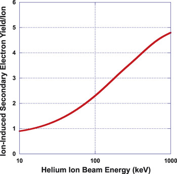
In order to be able to use Equation 3, appropriate numerical values for ε and λd must be obtained. ε is only a scaling constant, but λd greatly affects the shape and form of the iSE yield curve as a function of energy, and so accurate experimental values for δSE must be employed. This was done by empirically adjusting the ε, λd parameters so that the predicted IONiSE yields give the best fit to the tabulated experimental iSE yield data. Reference Lin and Joy6 A detailed compilation of iSE yields for a variety of elements and materials, and incident ions, is available. Reference Joy11 For example, a search of the data in the file provided iSE yield data as a function of the incident He+ beam energy for 29 different elements within the desired energy region of 10 keV to 100 keV. The λd value was then determined by finding the experimental value, which provided the best match to all the published data for the material. Figure 1 shows an example of fitted iSE yield data for a He+ beam on copper. Reference Ramachandra, Griffin and Joy7 In this case, two independent sets of yield measurements were available, both of which covered the energy range from 10 keV to 100 keV. The continuous line shows the computed best fit profile to the experimental data obtained by empirically fitting the data. In this case, the relevant parameters are λd = 9 Å and ε = 63 eV.
Example of fitted ion-induced secondary electron yield data for a 10 keV to 1000 keV He+ beam into C. The continuous line shows the computed best fit to two sets of experimental data. Reference Ramachandra, Griffin and Joy7

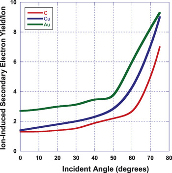
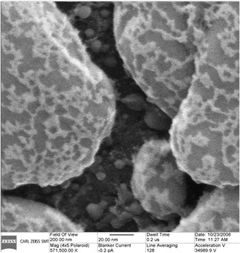
For elements where the required data have been obtained by fitting, it is now possible to accurately predict the variation of the magnitude of the ion-generated SE signal for any incoming ion as a function of the incident angle between the specimen and the ion beam for a given energy. This is important because it is this topographic variation of the signal yield as a function of the incident beam angle that is used to quantitatively determine the surface profile of structures in semiconductor device metrology and other nanoscale studies. Figure 2 compares the predicted variation of the iSE yield as a function of the incident beam angle for carbon, copper, and gold when using a 35 keV helium beam. Reference Ramachandra, Griffin and Joy7 Significant differences between these three computed profiles are readily seen. Figure 3 is an He+ image of a few layers of Au that appear bright on C (graphite) which appears dark, acquired with an operating voltage of 34.9 kV. The variations in iSE yield as a result of topography are clearly seen. Varying the incident beam energy will also change the relative signal levels from these and from all other elements.
Predicted variation in ion-induced secondary electron yield for a 35 keV He+ primary beam as a function of incident beam angle for C, Cu, and Au. Reference Ramachandra, Griffin and Joy7

He+ ion-induced secondary electron image of Au islands on C obtained at an operating voltage of 34.9 kV. Reference Ramachandra, Griffin and Joy7 Image courtesy of Carl Zeiss Inc.

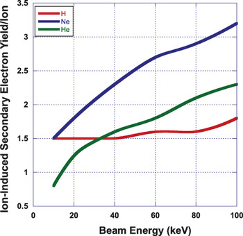
Although such data are of interest and value, they only represents a small step toward generating the much larger database, which will be required if ion beam microscopy is to become the state-of-the-art imaging method of choice, especially with newer ion sources coming online (see the article by Smith et al. in this issue). In that case, it is also necessary to be able to derive iSE yield curves, together with their fitting parameters, for all the solid elements in the periodic table as well as for both organic and inorganic compounds. Unfortunately, this exercise, while valuable, would also be very costly and time consuming. Fortunately, at least within sensible limits, such an effort is probably unnecessary. Current studies suggest that for the ions most likely to be of interest (H+, He+, Ar+, Ne+, and Ga+) once an optimally fitted set of data values has been generated for a given incident ion, data for the given target element or material—but using a different choice of ion beam—can then be predicted by simply repeating the simulation using the same ε, λd values as those applied previously but by now inserting the different ion type and stopping power parameters for the new choice of beam. Reference Seiler, Kaiser, Niedrig, Newbury and Shimizu9 Figure 4 shows an example of the application of this approach comparing the fitted iSE yield for He+ on copper, with the predicted iSE yields for copper when using Ne+ or H+ ions. Reference Ramachandra, Griffin and Joy7
A comparison of predicted ion-induced secondary electron (iSE) yields for H+, He+, and Ne+ at 10 keV to 100 keV into Cu demonstrating the change in iSE yield with incident ion type. Reference Ramachandra, Griffin and Joy7

Applications of iSE imaging with Ga ions
It has become quite common in FIB tools to form images using SEs induced by the Ga+ ion beam. These images show a large range of SE yields due to material contrast and channeling of the ion beam. The advantages of images formed by iSE are many. The first is that since there are no primary beam electrons, there are no backscattered electrons to reduce the contrast in the iSE signal, and the SE yield resulting from ion bombardment is much greater than that for electron-generated SE, thus allowing iSE images to be obtained faster with better signal-to-noise ratios. Reference Ishitani, Yamanak, Inai and Ohya12 The other major advantage of iSE over electron-generated SE is the much better contrast resulting from channeling of the ions in crystalline samples. These advantages are in contrast to the major disadvantages of iSE imaging of sample damage due to the high energy ion beam, including sputtering and ion implantation. It is not possible to avoid all damage to the sample when ions are used for imaging, but the damage can be minimized through careful choices of imaging parameters.
Various studies have been conducted to understand the material contrast produced by iSE in ion microscopy. One study of Ar+ and Ga+ concluded that the atomic number dependence of iSE was opposite that of electron induced secondary electrons (eSE), and iSE decreased monotonically with increasing atomic number. Reference Sakai, Yamada, Suzuki and Ichinokawa13,Reference Sakai, Yamada, Suzuki and Ichinokawa14 This conclusion was mostly a result of the limited selection of elements that was studied. Simulation of iSE yield has shown that it is not monotonic and demonstrates cyclical behavior associated with the filling of electron shells in the target. Further experimental and modeling research has shown the cyclical nature of the iSE yield with atomic number. Reference Giannuzzi and Utlaut15
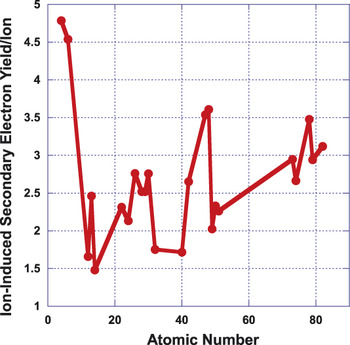
Material contrast in iSE imaging arises from differences in the yield of SEs. The IONiSE software was utilized to simulate the SE yields from elements that span the periodic table. The results are shown in Figure 5 . Reference Ramachandra, Griffin and Joy7 The predicted data in Figure 5 clearly demonstrate that there is not a monotonic relationship between the iSE and atomic number, as had been indicated by some published articles. The periodic behavior of the iSE yield as a function of atomic number leads to multiple elements with similar iSE yields. The current poor understanding of material contrast in iSE images leads to difficulty in interpretation of the information in an image. This can be contrasted with typical high-energy backscattered electron imaging in the scanning electron microscope (SEM), where the backscatter yield is generally observed to be a smooth monotonically increasing function of the target atomic number. One must be aware of the complicated relationship between iSE yields and atomic number when interpreting the image contrast in multi-element samples.
Predicted ion-induced secondary electron (iSE) yields as a function of target atomic number for 30 keV Ga+ ions. Note the lack of a clear monotonic relationship between the iSE yield and the atomic number of the target. Reference Ramachandra, Griffin and Joy7

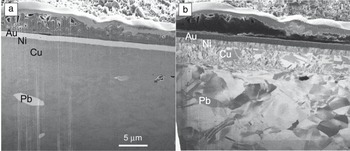
Figure 6 shows a pair of SE images acquired with electrons and Ga+ ions. In normal SEM, by eSE imaging of multi-element samples, the true material contrast may be altered by thin surface contamination films. That is not an issue in iSE, as the ion beam can be used to clean the surface of the sample to allow the true material contrast to be observed. In the images in Figure 6, the surface is a freshly prepared cross-section of a plated electronic contact. The sample consists of a leaded brass alloy that has been plated with Ni, Cu, and Au layers. The eSE contrast shown in Figure 6a is dominated by surface topography, atomic number contrast, and some channeling contrast. The increase in signal for the higher atomic number components is mostly due to the increase in the backscattered electron yield, resulting in an increased number of SEs. The ion image in Figure 6b shows the pure iSE signal, as there are no other electrons produced during the interaction of the ion beam with the sample. The complex nature of iSE yields, with respect to the atomic number, is obvious in this image, where the higher atomic number elements (Au and Pb) have lower iSE yields than Cu, Ni, and brass. Note the Pb inclusion and the Au plating on the surface that have high SE yields in the eSE image (Figure 6b) but lower iSE yields relative to the Ni and Cu plating at the surface of the sample. The contrasts observed in the iSE image do not entirely agree with the results of the IONiSE calculations that show that Pb and Au have somewhat higher iSE yields than Ni and Cu. Figure 6b demonstrates that iSE yield in crystalline materials depends markedly on the crystalline orientation of the substrate. The channeling contrast is essential for imaging grain contrast, but further complicates the interpretation of iSE images. Reference Giannuzzi and Michael16,Reference Michael17
Images of a plated brass electronic contact. (a) Electron-induced secondary electrons image at 5 keV. (b) Ga+ ion-induced secondary electron image acquired at an operating voltage of 30 kV.

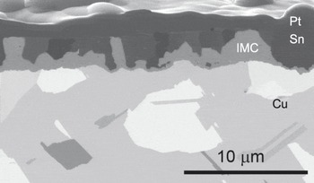
Figure 7 shows a cross-section of a Cu test coupon plated with Sn, which was held at room temperature for one year. During the aging time, the Sn interacts with the Cu to form an intermetallic compound at the interface between the Sn and the Cu. A Pt protective layer was applied to the sample during cross-section preparation. The iSE yield from Sn is lower than the yield from the Cu substrate, resulting in the Cu substrate appearing bright when compared to the Sn plating. The calculations in Figure 5 indicate that Sn has a lower iSE yield than does Cu, as observed in Figure 7. As was also shown in Figure 6, the channeling contrast again complicates materials contrast in the image.
Ga+ ion-induced secondary electron image of a focused ion beam cross-section of Cu plated with Sn acquired at an operating voltage of 30 kV. IMC is an intermetallic compound formed between Sn and Cu.

Conclusions
Imaging secondary electrons induced by ion beams in FIB instruments is becoming a common and valued imaging mode. A Monte Carlo model has been presented that can quantitatively interpret iSE yield data. The model requires the parameters of the semi-empirical model to be determined by fitting to experimental yield data, and so the validity of the result depends completely on the quality of the experimental data used. The model was used to predict contrast that can be observed for topographic variation of the signal yield as a function of the incident beam angle, which is used to quantitatively determine the surface profiles of structures in semiconductor device metrology and other nanoscale studies. This Monte Carlo model also predicts that the iSE yield is not a smooth monotonic function of atomic number of the target resulting in difficult to interpret materials contrast. Imaging of multi-element targets with Ga+ ions has shown that the model is useful for understanding materials contrast. Further work is needed to fully characterize iSE imaging and yields so that materials contrast is more easily interpreted. Furthermore, channeling contrast in crystalline samples complicates image interpretation, and future studies of iSE should include consideration of crystalline targets. When topographical contrast, material contrast, and channeling contrast are fully understood, then ion microscopy can move forward as a quantitative microstructural tool.
Acknowledgments
Sandia National Laboratories is a multiprogram laboratory operated by Sandia Corporation, a wholly owned subsidiary of Lockheed Martin Company, for the US Department of Energy’s National Nuclear Security Administration under contract DE-AC04–94AL85000.