Introduction
During the last decade, the rapid growth in wireless communication demanded for miniaturized electronic devices with multiband applications [Reference Xu, Wu and Wei1]. Because of this, multiband filter became an interesting subject of research. Since the conventional microstrip band-pass filters are facing a problem of large dimensions, they are not suitable for integrating with miniaturized modern electronic devices. In order to achieve miniaturization, metamaterial (MTM) structures are preferred by using resonant approach (split ring resonator and complementary split ring resonator) and composite right/left handed (CRLH) transmission line (TL) approach [Reference Caloz and Itoh2–Reference La and Lu4]. MTMs are artificially designed periodic structure, which follows homogeneity condition and provide exceptional electromagnetic characteristics such as negative refractive index, zero propagation constant, and antiparallel group and phase velocity [Reference Choudhary and Chaudhary5].
Several concepts have been described in the literature [Reference Cho and Yun6–Reference Li, Huang, Wang and Zhao17] to design a dual-band band-pass filter. In 2013, Cho et al. [Reference Cho and Yun6] utilized an asymmetrical coupled line to design a dual-band band-pass filter. In this configuration, the suggested asymmetric coupled line offers an improvement in the common mode suppression level without the use of lumped element or stubs and this results in a dual-band band-pass response on differential mode signals. Another dual-band band-pass filter, which is designed with the cascading of band-pass and band-stop filter, has been reported in [Reference Tsai and Hsue7]. In this configuration, the cascaded band-pass and band-stop filter structures are designed with a serial shunted line configuration and coupled serial shunted line structures. In this structure by controlling the individual characteristics of both cascaded band-pass and band-stop filter both the pass-bands can be controlled. A hybrid structure resonator-based dual-band band-pass filter with high selectivity and multi-transmission zero has been reported in the literature [Reference Ieu, Zhang and Zhou8]. In this structure a hybrid resonator is configured with microstrip rectangular rings and patch. Microstrip rings have been used for exciting the microstrip patch. Additionally, it also works as a resonator. This configuration offers multiple transmission zeros (11), along with good selectivity and better out of band rejection. The electrical size of all these filter structures is nearly half of the wavelength.
Further, few miniaturized dual-band band-pass filters have been claimed in [Reference Wang, Tang, Wu, Yu, Zhang and Wang11–Reference Li, Huang, Wang and Zhao17]. Wang et al. [Reference Wang, Tang, Wu, Yu, Zhang and Wang11] claimed a complementary split ring resonator and a quarter-mode substrate-integrated waveguide-based compact dual-band filter. Dual-band characteristic has been generated by combining two different sizes of quarter-mode substrate-integrated waveguide. The use of complementary split ring resonator increases the electrical length and results in miniaturized filter structure. Literature [Reference Balalem, Machac and Omar12] utilizes a square loop dual-mode resonator to convert a broadband band-pass filter into dual-band band-pass filter. This can be understood with the fact that the use of a dual-mode resonator introduces transmission zero in the passband of broadband band-pass filter. It offers compact size with better rejection between bands. In [Reference Xu and Zhang13], a dual-band band-pass filter has been designed using a frequency selective coupling structure-loaded stepped impedance resonator. This configuration results in a compact filter design with wide stop-band. A dual-band band-pass filter using a stub-loaded open and short circuited λ/4 resonator has been reported in [Reference Zhang, Chu and Chen14]. In this configuration the coupling-loaded stub effectively controls the bandwidth and frequency of operation and results in a compact filter structure with better mutual band isolation. Jang et al. [Reference Jang and Kahng15] utilized the concept of zeroth order resonance (ZOR) to design a miniaturized dual-band band-pass filter which can be used for ISM and GSM applications. ZOR, an exceptional property of CRLH-TL, offers high level of miniaturization (less than quarter wavelength) as compared to the conventional filters.
A miniaturized open-ended CRLH-TL-based dual-band band-pass filter with series stepped capacitance and shunt meandered line inductance has been designed and discussed in this paper. The presented band-pass filter has been applied with open-ended boundary conditions, so shunt parameters are key elements for the justification of ZOR mode. Further, the designed filter structure utilizes coplanar waveguide feeding arrangement to reduce the design complexity and offers uniplanar configuration. The MTM behavior for the presented filter structure has been justified with the help of dispersion plot.
Design analysis and modeling
Distinct developing steps for designed filter structure
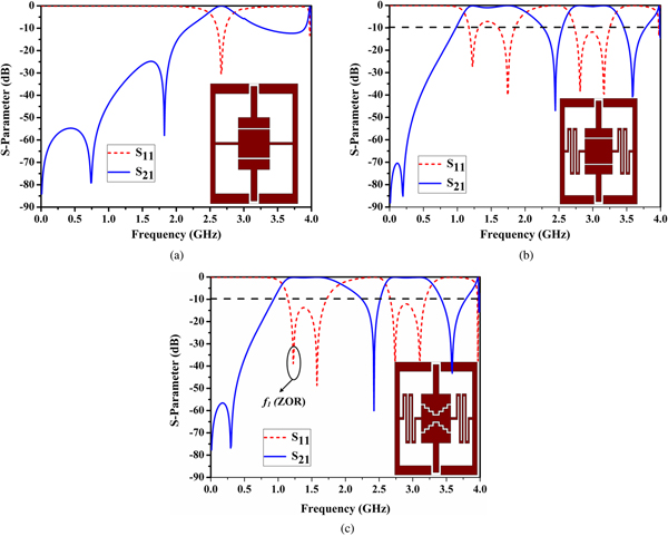
The design process of the proposed filter structure utilizes the concept of CRLH-TL. Initially, a simplified CRLH-TL-based filter structure has been designed as shown in Fig. 1(a). Since the designed filter has been applied with open-ended boundary conditions, it is a well-known fact that its shunt parameters (shunt inductance and capacitance) play a crucial role in defining ZOR properties [Reference Choudhary and Chaudhary5, Reference Jang, Choi and Lim18], discussed in the section ‘Equivalent circuit modeling, dispersion relation, and proof of ZOR’.
Distinct developing steps for the designed filter structure. (a) Simplified CRLH-TL-based filter, (b) meandered line-integrated filter structure, and (c) proposed filter structure.

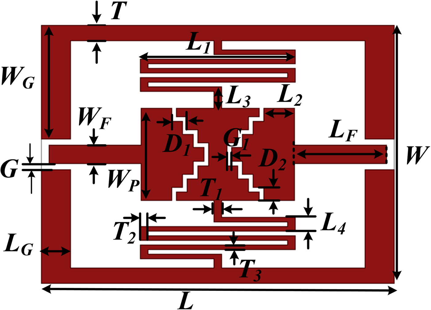
In order to improve the value of shunt inductance meandered line structure has been incorporated, as shown in Fig. 1(b). Further, meandered inductance has been optimized to achieve a dual-band band-pass response. Additionally, stepped series capacitance has been introduced to improve the impedance matching, as shown in Fig. 1(c). The layout of the designed dual-band band-pass filter with its optimized dimensions is shown in Fig. 2.
Layout of the designed dual-band band-pass filter with optimum dimensions. All aspects are in mm: L = 23, L 1 = 10.1, L 2 = 2, L 3 = 1.4, L 4 = 0.9, L F = 6, L G = 1.9, W = 16.8, W G = 7.4, W F = 1.2, W P = 6, T = 1, T 1 = 0.5, T 2 = 0.5, T 3 = 0.3, D 1 = 1, D 2 = W P/7, G = 0.4, G 1 = 0.3.

Equivalent circuit modeling, dispersion relation, and proof of ZOR
The design equivalent circuit diagram corresponding to the designed dual-band band-pass filter is shown in Fig. 3. The designed filter structure has been configured with the stepped capacitance within patch and meandered line inductance, responsible for left-handed capacitance (C L) and inductance (L L), respectively. Further, right-handed inductance (L R1) is associated with the feedline and patch connected to feedline while L R2 is associated with the center patch which is connected to the meander line inductor. Right-handed capacitance (C R) is associated with the gap between patch and ground connected strip. Further, separation between feed-line and Coplanar waveguide (CPW) ground plane originates a capacitance in parallel which is indicated by C C. In order to extract the lumped parameter values of the equivalent circuit advance design system circuit simulator has been used. The extracted lumped parameter values of the designed filter structure are as follows: L R1 = 23 nH, L R2 = 13.2 nH, L L = 3.4 nH, C L = 0.4 pF, C R = 3.0 pF, and C C = 1.96 pF.
Equivalent circuit diagram for the deigned filter configuration.

In order to discuss the dispersion relation for the designed dual-band band-pass filter, Bloch-Floquet theorem along with evaluated immittances of the equivalent circuit diagram has been utilized. According to Bloch-Floquet theorem the dispersion relation can be expressed as equation (1) [Reference Kumar, Choudhary and Chaudhary3]:
 $$\beta (\omega ) \times d = \cos ^{-1}(1 + Z(\omega )Y(\omega ))$$
where d stands for the physical length of the unit cell and β(ω) is a propagation constant.
Further, Z(ω) indicates series impedance while Y(ω) stands for the shunt admittance of the equivalent circuit diagram for the designed dual-band band-pass filter:
 $$\eqalign{ Z & = j\omega L_{R1} + j\omega L_{R2} + \displaystyle{1 \over {\,j\omega C_L}} = \displaystyle{{1-\omega ^2(L_{R1} + L_{R2})C_L} \over {\,j\omega C_L}}} $$
and
 $$\eqalign{Y & = j\omega \lpar {C_R + C_C} \rpar + \displaystyle{1 \over {\,j\omega L_L}} = \displaystyle{{1-\omega ^2L_L\lpar {C_R + C_C} \rpar } \over {\,j\omega L_L}}.} $$
The resonance mode for the proposed dual-band band-pass filter can be achieved with the help of dispersion relation, by equation (2):
 $$\beta (\omega ) \times d = n\pi \quad (n = 0, \pm 1, \pm 2, \ldots, \pm (N-1))$$
where n represents mode number and N indicates total number of unit cells. At the frequency of ZOR, n = 0, so from equation (2) β = 0. It reveals that at the frequency of ZOR, infinite wavelength propagation is possible. Therefore ZOR offers miniaturization property. By using equations (1) and (2) at ZOR frequency:
 $$Z(\omega )Y(\omega ) = 0$$
 $$\omega ^4-\omega ^2\lsqb {\omega_{se}^2 + \omega_{sh}^2} \rsqb + \omega _{se}^2 \omega _{sh}^2 = 0$$
 $$\omega ^2 = \omega _{se}^2 \; {\rm or} \; \omega _{sh}^2 $$
 $$\omega = \pm \! \omega _{se}, \pm \! \omega _{sh}$$
where
 $$\omega _{se} = \displaystyle{1 \over {\sqrt {C_L\lpar {L_{R1} + L_{R2}} \rpar }}} $$
and
 $$\omega _{sh} = \displaystyle{1 \over {\sqrt {L_L\lpar {C_R + C_C} \rpar }}}. $$
Based on the applied boundary condition the ZOR frequency can be defined either by ω se or by ω sh.
In case of open-ended boundary condition, the input impedance of the resonator is inversely proportional to the product of shunt admittance (Y) and number of unit cells (N) as shown in equation (4):
 $$Z_{in}^{open} = -jZ_0\cot \lpar {\beta l} \rpar \mathop \approx \limits^{\beta \to 0} \displaystyle{1 \over {NY}}$$
Hence, the ZOR frequency for open ended boundary condition can be estimated by equation (5):
 $$\omega _{ZOR} = \omega _{sh} = \displaystyle{1 \over {\sqrt {L_L\lpar {C_R + C_C} \rpar }}} $$
Similarly, in case of short ended boundary condition, the input impedance of the resonator is proportional to the product of series impedance (Z) and number of unit cells (N), as shown in equation (6):
 $$Z_{in}^{short} = jZ_0\tan \lpar {\beta l} \rpar \mathop \approx \limits^{\beta \to 0} NZ$$
In this case the ZOR frequency can be estimated by equation (7):
 $$\omega _{ZOR} = \omega _{se} = \displaystyle{1 \over {\sqrt {C_L\lpar {L_{R1} + L_{R2}} \rpar }}} $$
The designed filter structure is configured with the open ended boundary condition so in this case the ZOR frequency can be estimated by shunt parameters, as equation (5). Apart from this, dispersion relation can also be estimated with the help of scattering parameters as shown in equation (8) [Reference Kumar, Choudhary and Chaudhary3, Reference Borja, Belenguer, Cascon, Esteban and Boria19]:
 $$\beta (\omega ) \times d = \cos ^{-1}\left( {\displaystyle{{1-\mathop S\nolimits_{11} \mathop S\nolimits_{22} + \mathop S\nolimits_{12} \mathop S\nolimits_{21}} \over {2 \times \mathop S\nolimits_{21}}}} \right)$$
where S 11 and S 22 represent reflection coefficients and S 12 and S 21 indicate transmission coefficients for any two-port network.
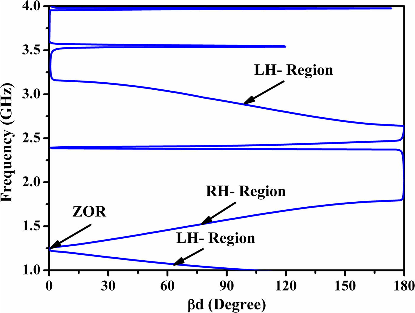
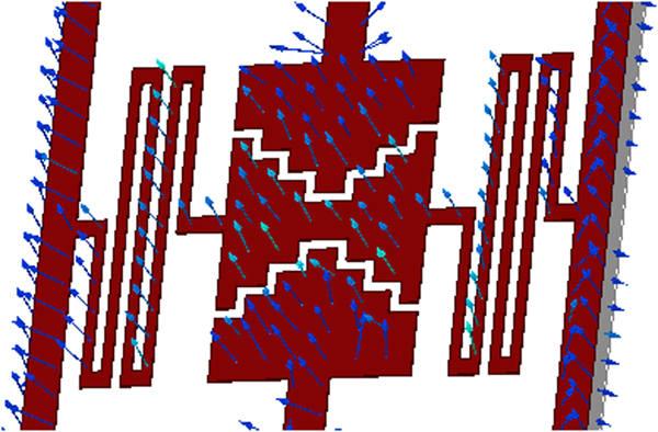
In order to discuss the MTM property for the designed dual-band band-pass filter, equation (6) has been utilized. Fig. 4 depicts the simulated dispersion curve for the designed dual-band band-pass filter. It can be clearly seen that the dispersion graph is divided mainly into two zones. LH and RH regions indicate the zones, where the dispersion curve shows negative and positive slopes, respectively. Simulated working bands (1.06–1.92 and 2.59–3.29 GHz) of the designed filter structure have two LH regions, from 1.06–1.24 to 2.62–3.29 GHz. It can also be observed that βd becomes zero at 1.24 GHz, which indicates the presence of ZOR at its first resonance frequency f 1. Further, the justification of ZOR frequency has been also given with the vectored electric field diagram, shown in Fig. 5. It is observed that almost no phase variation occurs throughout the patch of the designed dual-band band-pass filter structure; therefore f 1 is the ZOR frequency [Reference Jang, Choi and Lim18–Reference Mishra and Chaudhary21].
Simulated dispersion plot for the designed dual-band band-pass filter.

Vectored E-field distribution on the active area of the designed dual-band-band-pass filter at the ZOR frequency of 1.24 GHz.

Parametric variation and quality factor analysis
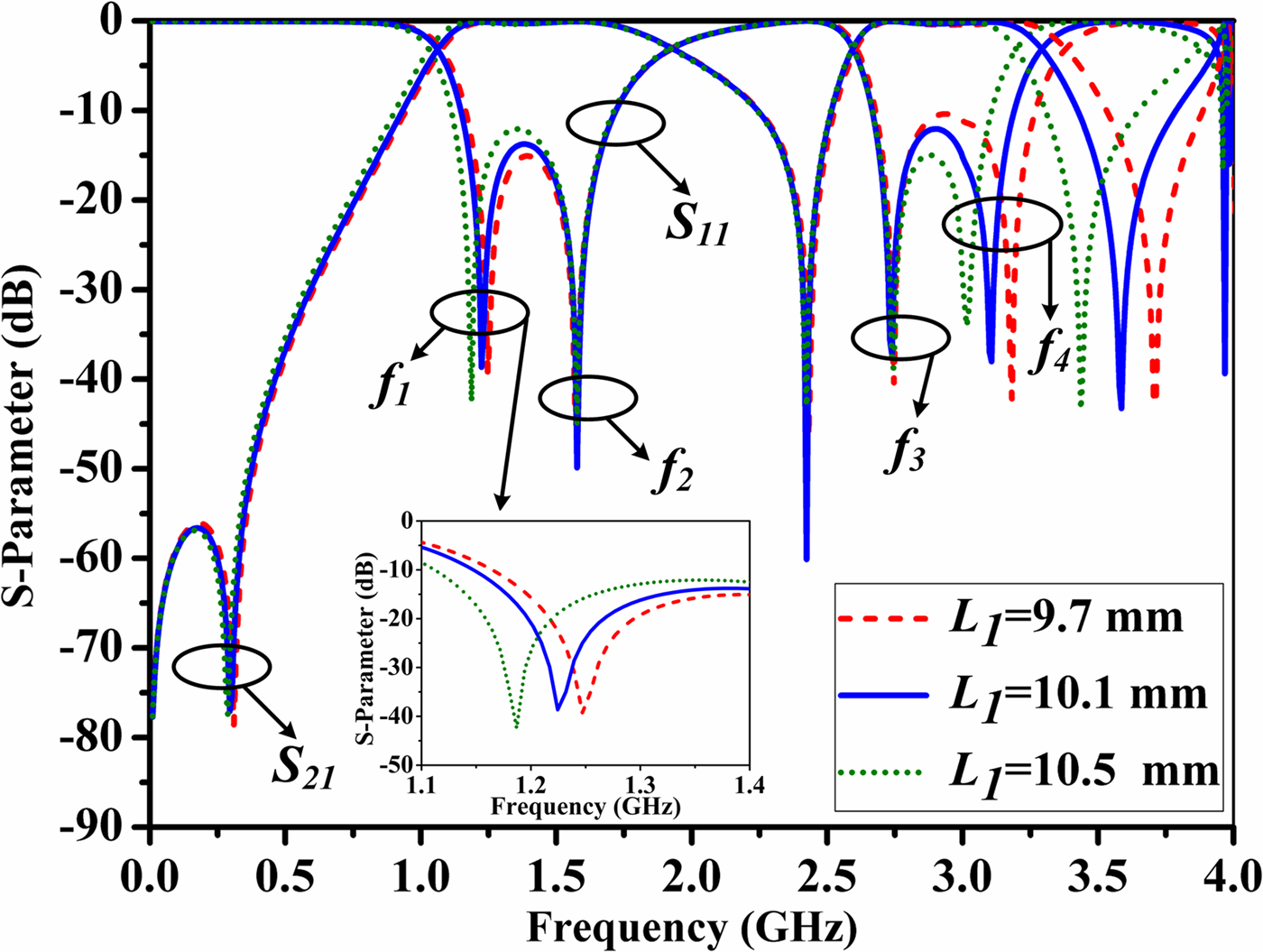
In simulated scattering parameters response at distinct values of L 1 is depicted in Fig. 6. It is perceived that by increasing L 1 from 9.7 to 10.5 mm, the resonance peaks f 1 and f 4 start moving toward lower frequency while f 2 and f 3 remains fixed. This shift in f 1 and f 4 can be explained with the increment in left-handed inductance associated with L 1.
Simulated scattering parameter response at distinct values of L 1.

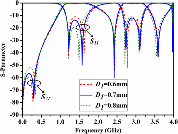
Figure 7 shows the variation in scattering parameter responses at different values of D 1. It is observed that by varying D 1 from 0.6 to 0.8 mm the series capacitance increases and results in the decrement of resonance frequencies f 2 and f 3, while resonance frequencies f 1 and f 4 (a minute shift) are almost unaffected. Further, from the above discussion it can be concluded that the resonance frequencies f 1 and f 4 can be effectively controlled by shunt parameter L 1 while resonance frequencies f 2 and f 3 can be effectively controlled by series parameter D 1. The above two optimizations can be utilized to explain the ZOR phenomena as discussed in equation (5).
Simulated scattering parameter response at distinct values of D 1.

Selectivity of any filter structure is an important parameter which defines the ability of filter to reject the frequencies beyond the 3 dB points. Better selectivity can be achieved by the higher quality factor. In order to calculate the unloaded quality factor, Eigen mode solver of HFSS 14.0 3D-simulation software is used [Reference Rathore, Awasthi and Biswas22].
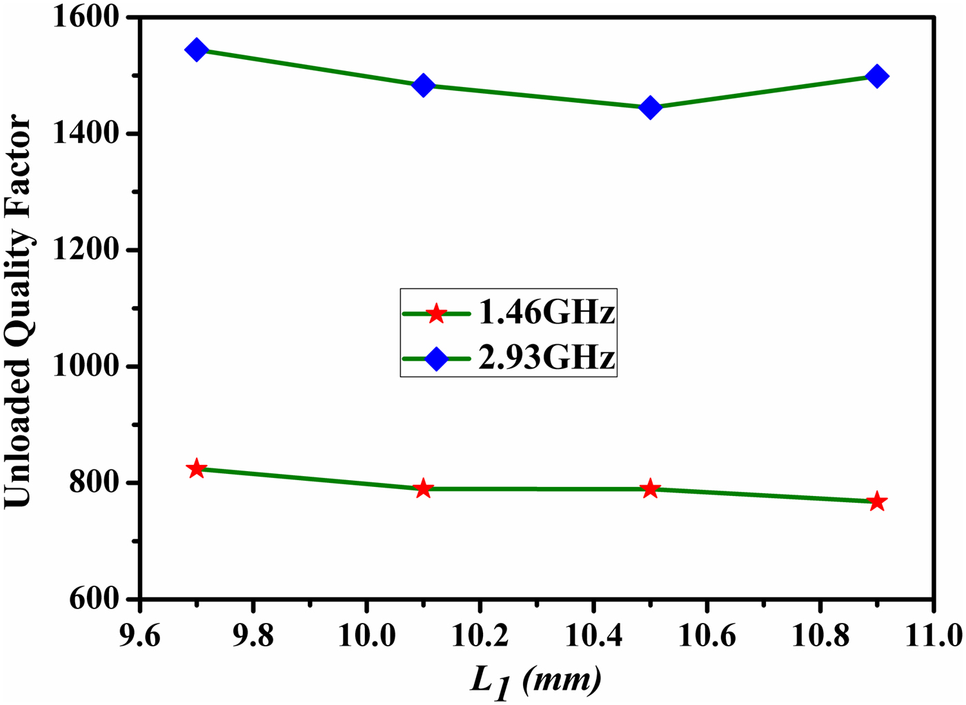
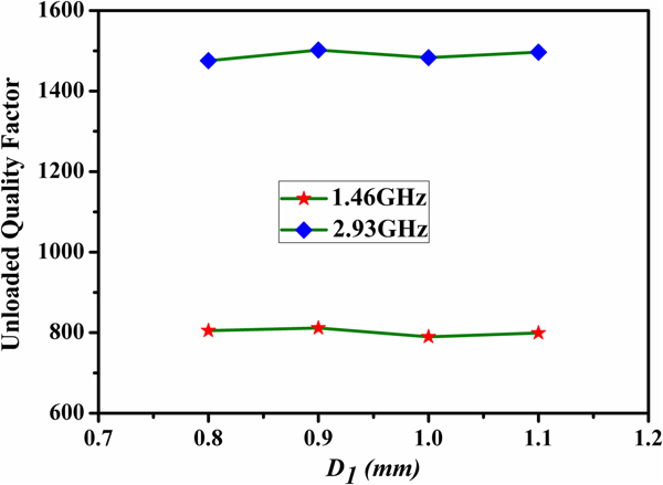
Figure 8 depicts variation in unloaded quality factor for the designed filter structure at different values of L 1. The unloaded quality factor graph has been plotted at the center frequencies (1.46 and 2.93 GHz) of both the passbands. Similarly, variation in quality factor at both the center frequencies at distinct values of D 1 for the designed filter structure is shown in Fig. 9. The designed filter structure offers a higher values of unloaded quality factor Q Ul = 789.91 and 1483.2 at center frequencies (simulated) of 1.49 and 2.94 GHz. It is a well-known fact that higher quality factor results in better selectivity. From the above discussion it is clear that by varying the parameters L 1 and D 1 the resonance frequencies can be controlled but at the same time the designed filter persists its excellent selectivity.
Simulated unloaded quality factor at various values of L 1.

Simulated unloaded quality factor at various values of D 1.

Measured results and discussion
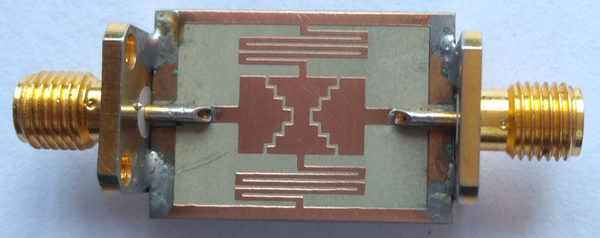
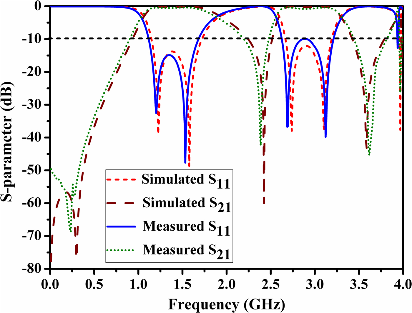
Figure 10 depicts the fabricated prototype for the designed dual-band band-pass filter. The designed filter structure has been printed on the single-sided copper (thickness = 0.035 mm) coated Rogers/RT Duroid 6010 (ε r = 10.2, thickness = 1.27 mm) substrate. Coplanar waveguide feeding arrangement has been utilized to provide excitation for the designed filter structure. The designed filter structure shows miniaturization with an overall footprint area of 0.26λ g × 0.19λ g, where λ g is the guided wavelength at the center frequency of 1.46 GHz. In order to validate the simulated and measured scattering parameters Fig. 11 is presented. It shows almost a similar type of pattern for scattering parameters. Little deviation in response may be because of the fabrication imperfection, connector losses, and non-uniformity of the substrate. The graph presents a dual-band band-pass response with 58.90 and 25.93% measured 3 dB bandwidth and 57.72 and 23.80% simulated 3 dB bandwidth. In addition to above it depicts input reflection coefficient better than −14 and −10 dB in both the passbands. Similarly, maximum simulated and measured transmission coefficients in the first pass band are −0.09 and −0.49 dB, respectively. In the second passband, the maximum simulated and measured transmission coefficients are −0.06 and −0.52 dB, respectively. Further, the designed filter structure offers rejection better than 40 dB between two passbands. 3 dB cut-off frequencies for the designed filter structure are at 1.03 and 1.89 GHz for the first passband and at 2.55 and 3.31 GHz for the second passband.
Fabricated prototype for the designed dual-band band-pass filter.

Simulated and measured scattering parameter response.

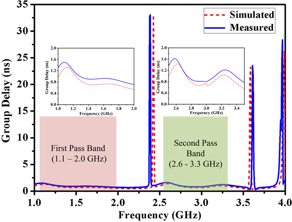
Figure 12 depicts simulated and measured group delay responses for the proposed filter structure. Group delay is an important parameter for designing any filter structure. It indicates the rate of change of transmission phase angle with respect to frequency [Reference Pozar23]. The group delay curve for the designed filter structure offers almost flat response throughout the passbands, which indicates a smooth transmission with a negligible amount of distortion. The designed filter structure offers average simulated and measured group delays of 0.83 and 1 ns, respectively, for the first passband and 0.93 and 1.07 ns, respectively, for the second passband. The maximum fluctuation in the simulated and measured group delays within the first band is from 0.57 to 1.32 ns and 0.75 to 1.49 ns, respectively. Similarly, the maximum variation in simulated and measured group delays is from 0.64 to 1.42 ns and 0.79 1.62 ns, respectively.
Simulated and measured group delay response for the designed dual-band band-pass filter.

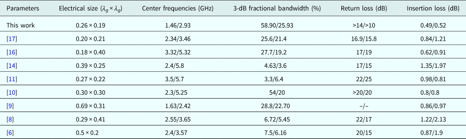
Table 1 shows the comparative study of this work with the previously published work. It can be observed that the proposed filter structures offer maximum 3 dB fractional bandwidth as compared with the articles mentioned in the table. In the given table, except for article [Reference Li, Huang, Wang and Zhao17], the designed filter structure provides the smallest electrical size. This miniaturization is achieved because of the MTM approach. Apart from this, the designed filter structure has the smallest insertion loss.
Comparison of this work with previously published articles

Conclusion
This paper presents a miniaturized open-ended dual-band band-pass filter with series stepped capacitance and shunt meandered line inductance for microwave frequency applications. The proposed filter structure has been designed with CPW feeding arrangement, which allows a uniplanar configuration with ease of fabrication. MTM property for the designed filter structure has been discussed using dispersion plot. The designed filter structure offers miniaturization with an overall electrical size of 0.26λ g × 0.19λ g, where λ g is the guided wavelength corresponds to the center frequency of 1.46 GHz. The designed filter structure offers measured −3 dB fractional bandwidth of 58.90% (1.03–1.89 GHz) and 25.93% (2.55–3.31 GHz) around the center frequency of 1.46 and 2.93 GHz, respectively. There are several wireless applications such as global navigation satellite system (1.559–1.610 GHz), GSM1800 (1.7–1.8 GHz), Wi-MAX (2.5–2.7 GHz), and naval radar and air traffic control (2.7–2.9 GHz), where the designed filter structure can be suitably used.
Author ORCIDs
Dilip Kumar Choudhary, Raghvendra Kumar Chaudhary http://orcid.org/0000-0001-5450-4034, http://orcid.org/0000-0001-6186-4089, Naveen Mishra http://orcid.org/0000-0003-2602-0731
 Naveen Mishra was born in Deoria (Uttar Pradesh), India on October 4, 1990. He received his B.Tech. degree in electronics and communication engineering from Uttar Pradesh Technical University, Lucknow in 2010. Currently, he is pursuing his Ph.D. from the Department of Electronics Engineering, Indian Institute of Technology (Indian School of Mines), Dhanbad, India. He joined the Department of Electronics Engineering, Indian Institute of Technology (Indian School of Mines), Dhanbad, in January 2014, as a Junior Research Fellow, where he has been a Senior Research Fellow since January 2016. He has authored or co-authored more than 24 research articles in international/national journals/conference proceedings. His current research interests involve metamaterial structures and its applications. He is an active student member of IEEE society and also serving as a reviewer in the International Journal of Electronics Letters.
 Mr. Dilip Kumar Choudhary was born in Purnea, Bihar, India. He is pursuing his Ph.D. from the Department of Electronics Engineering, Indian Institute of Technology (Indian School of Mines), Dhanbad, India and receiving fellowship from MHRD, Government of India. He did his M.E. degree from the Birla Institute of Technology, Ranchi, India in 2012, where he received fellowship from MHRD, Govt. of India. He has done his B.Tech. degree from Biju Patnaik University, Orissa, India in 2009. He has authored more than 21 referred Journal and Conference papers. He was the recipient of the International Travel Grant form DST, India for presenting a paper in 2017 IEEE Asia Pacific Microwave Conference (APMC), Kuala Lumpur, Malaysia. He was the recipient of the Best Student Paper (Third Position) at Progress in Electromagnetics Research Symposium (PIERS), Singapore in 2017. He is a student member of IEEE. His current research interests includes metamaterial and its application in filter, antenna, and absorber.
 Dr. Raghvendra Kumar Chaudhary is working as an Assistant Professor at the Department of Electronics Engineering, Indian Institute of Technology (ISM), Dhanbad, India. He did his Ph.D. from IIT Kanpur, India in January 2014, M.Tech. degree from IIT (BHU), Varanasi, India, in 2009, and B.Tech. degree from UIET Kanpur India, in 2007. His current research interests include dielectric resonator antenna, metamaterial antenna, MIMO antenna, and metamaterial absorber. Dr. Chaudhary has authored over 75 international journal papers and 80 conference papers. Dr. Chaudhary has served as Chair, IEEE Student Branch, Uttar Pradesh Section, in 2012 and 2013, respectively. He was recipient of many best paper awards in various conferences such as IEEE APACE Malaysia, PIERS Singapore, ATMS, India, etc. He has also started 2-Year M.Tech. Course Program in RF & Microwave Engineering at the Department of Electronics Engineering, IIT (ISM), Dhanbad. He is Associate Editor of IEEE Access, Senior Member of IEEE, and potential reviewer of many journals and conferences such as IEEE TAP, IEEE AWPL, IET MAP, IET Electronics Letters etc. He is presently handling many research projects in the capacity of Principal Investigator sponsored from different funding agencies such as SERB (DST), ISRO, TEQIP, etc.