I. INTRODUCTION
Cu metallization in Si devices has been widely used for its high electrical conductivity and large resistance to electromigration. However, Cu readily reacts with Si at low temperatures even below 200 °C, which results in device failures.Reference Liu and Chen1–Reference Chu and Lin3 The presence of a thin native SiO2 on the surface of Si cannot inhibit Cu diffusion, and silicide is formed above 625 K.Reference Zhou, Gustafsson and Garfunkel4 Diffusion barrier layers such as Ta, Ta/TaN, (TiVCr)N, AlCrRuTaTiZr, and Co(W,P) have to be used to prevent Cu from diffusing into the transistor region and from forming Cu3Si.Reference Chu, Yu, Wu, Lin, Wang and Chen5−Reference Kohn, Eizenberg and Shacham-Diamand9 With the feature size of interconnect shrinking, the fabrication of a barrier structure with good thermal stability and small dimension is becoming more and more challenging.Reference Chu, Yu, Wu, Lin, Wang and Chen5,Reference Wang, Dong and Jiang10–Reference Lin, Chu, Mahalingam, Lin and Wang12 Alternatively, there is also a barrierless scheme where the Cu seed layer is alloyed with Ru, W, Nb, and Mo to enhance the diffusion barrier property.Reference Chu, Lin and John2,Reference Chu and Lin3 These elements all have large positive enthalpies of mixing with Cu so that they have very limited solid solubilities in Cu. The solute segregation and precipitation retard recrystallization and grain growth.Reference Chu and Lin3 Consequently, the enhanced chemical stability is often accompanied by a poor electrical conductivity. The full dissolution of a proper amount of the diffusion-inhibiting elements in Cu would produce enhanced chemical stability. Such a single-phase state would also allow easy defect annihilation and stress release upon annealing, which counterbalances the possible increase in electrical resistivity due to alloying. The latter factor is particularly important for thin films deposited by sputtering that generally contain extensive structural defects and large stresses. Such alloyed Cu films, serving as the seed layer for further Cu plating, can be deposited directly on the dielectric substrate, without resorting to any barrier layer. Cu(Nb) thin films containing various amounts of insoluble Nb (up to 24.7 at.%) have been investigated as reported in the literature.Reference Mahalingam, Lin, Wang and Chu13 The films containing 2.7 at.% Nb showed the least electrical resistivity, about 5 μΩ cm, for all the annealing temperatures, which is still too high for the industries.
A possible way to dissolve an insoluble diffusion-inhibiting element in Cu would be to introduce a third element, which is both soluble with the diffusion-inhibiting element and with the solvent Cu. Such an alloying principle has been used in interpreting the optimum Fe contents in Cu–Ni industrial alloysReference Zhang, Wang, Wang, Li, Wen and Dong14: Fe, being insoluble with Cu (the large positive enthalpy of mixing between Fe and Cu signifying the Fe and Cu nearest neighbor is not favored), is dissolved in Cu–Ni via Ni which is both soluble with Cu (the weak positive enthalpy of mixing between Ni and Cu) and with Fe (the weak negative enthalpy of mixing between Ni and Fe favoring Fe–Ni nearest neighbors). A nearest-neighbor structural model was thus established, where atoms are so arranged that they satisfy in an ideal manner their nearest neighbor interactions. The solute Fe would tend to be surrounded completely by twelve Ni atoms (the nearest neighbor coordination polyhedron in the face centered cubic [FCC] structure is cuboctahedron with coordination number 12, formulated as [Fe–Ni12]) for their weak negative enthalpy of mixing. The [Fe–Ni12] cuboctahedral clusters would then be scattered in a Cu matrix. In this way, the unfavorable Fe–Cu nearest neighbor is avoided. Such a solid solution should have a high structural stability and can be formulated by [Fe–Ni12]Cux, in analogy to the cluster-plus-glue-atom model initially developed for quasicrystals and for bulk metallic glasses.Reference Dong, Wang, Qiang, Wang, Jiang, Han, Li, Wu and Xia15 Actually, this model describes the short-range order structural feature of a solid solution, in terms of the nearest neighbor cluster [Fe–Ni12] and glue atoms Cu. In a general sense, in accordance with the cluster-plus-glue-atom model for stable solid solutions,Reference Zhang, Wang, Wang, Li, Wen and Dong14 any solid solution with a high short-range-order stability is composed of a nearest-neighbor cluster part and a glue atom part. The cluster refers to the nearest neighbor coordination polyhedron (cuboctahedron with coordination number 12 for FCC and rhombic dodecahedron with coordination number 14 for body centered cubic [BCC] structure) and is composed of elements with negative enthalpies of mixing, whereas the glue atoms refer to those atoms that are situated outside the clusters in the structure and usually have weaker enthalpies of mixing with the cluster shell atoms (mainly the solvent).
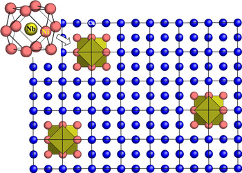
Likewise, this model was used in designing Cu–Ni–Mo films, where Mo was dissolved in Cu with the aid of Ni, and the films with an Mo/Ni ratio of 1/12 exhibited a low electrical resistivity in combination with high thermal stabilities against silicide formation.Reference Li, Liu, Zhang, Chu, Wang and Dong16 In this paper, we deal with a similar system Cu–Ni–Nb, where Nb plays the same role as Fe, and Mo:Nb has a large positive enthalpy of mixing with Cu and hence is insoluble in Cu; Ni shows weak enthalpies of mixing both with Nb and with base Cu so that the solubility of Nb in Cu is enhanced in the presence of the third element Ni. The cluster-plus-glue-atom model describing the short-range order feature of a stable solid solution Cu–Ni–Nb is shown in Fig. 1. This idealized short-range-order structure is characterized by Nb-centered cuboctahedral clusters [Nb–Ni12] scattered in a Cu matrix. The clusters do not show any overlapping to avoid the development of the nearest neighbor of the type Nb–Ni into longer-range ones like Nb–Ni–Nb–Ni. A structure satisfying ideally the nearest-neighbor configuration (Ni/Nb = 12/1) as demanded by the enthalpies of mixing between the constituent elements should naturally possess a high thermal stability. When Ni/Nb > 12/1, the extra amount of Ni above the ideal ratio of 12/1 would be mixed with matrix Cu and form Cu–Ni solid solution. However, when Ni/Nb < 12/1, the excessive Nb would not be in solution with Cu and the precipitation of Nb would occur.
Cluster-plus-glue-atom model of a [Nb–Ni12]Cux stable solid solution, where Nb-centered and Ni-shelled cuboctahedral clusters [Nb–Ni12] are scattered in a Cu matrix.

In the following, Cu–Ni–Nb ternary films will be prepared by magnetron sputtering on barrierless Si(100) substrates and will be characterized for microstructure, electrical conductivity, and thermal stability.
II. EXPERIMENTAL PROCEDURE
To experimentally obtain the tentative compositions formulated by [Nb–Ni12]Cux, Ni–Nb alloys with five different Ni/Nb atomic ratios, Ni12Nb0.5, Ni12Nb1, Ni12Nb1.5, Ni12Nb2, and Ni12Nb2.5, were prepared by arc melting and copper-mould suction-casting in argon atmosphere in identical conditions. Alloy slices, 3 mm in diameter and 1 mm in thickness, were pasted onto a pure Cu magnetron sputtering target with a conductive adhesive. By cosputtering the Cu target and the Ni–Nb slices, Cu–Ni–Nb films with different Ni/Nb ratios were deposited onto Si(100) wafers. No intentional heating of the substrate was applied during the deposition. The substrate wafers prior to the deposition experiments were first ultrasonically cleaned in acetone, ethanol, and deionized water, then treated by an immersion in a 5% HF solution for 3 min, and finally dried with nitrogen gas.
Isothermal annealings were performed in a vacuum of 10−5 Pa for 1 h, at temperatures ranging from 400 to 700 °C. For a long-term thermal stability evaluation, 8 cycle annealings at 500 °C (5 h per cycle) were also carried out, reaching a total annealing time of 40 h. Sheet resistances were measured with the four-point probe method as already stated in Ref. Reference Nie, Li, Chu, Wang, Lin and Dong17. The base resistivity of Si is 6–9 Ω cm. Crystallographic and microstructural studies of the films were carried out using grazing-angle incidence x-ray diffraction (XRD) with a grazing angle of 1° (Cu Kα, out-of-plane mode) and transmission electron microscopy (TEM). The compositions were measured by an electron probe microanalyzer.
III. RESULTS AND DISCUSSION
The Cu contents in all the films deposited with one Ni–Nb slice are substantially equal, about 99.7 at.% Cu. Though the total amount of Ni and Nb is about 0.3 at.%, the measured Ni/Nb ratios of the films and the designed Ni/Nb ratios in the slices are slightly different, Ni being richer in the films. This is due to the different sputtering rates of Ni and Nb, which are related to the target material, the bias of bombarding ions, and the deposition pressure.Reference Tian and Liu18 The films deposited with the nominal Ni/Nb ratios of Ni12Nb0.5, Ni12Nb1, Ni12Nb1.5, Ni12Nb2, and Ni12Nb2.5 respectively have their measured compositions of (Nb0.4/12.4Ni12/12.4)0.3Cu99.7, (Nb0.9/12.9Ni12/12.9)0.3Cu99.7, (Nb1.2/13.2Ni12/13.2)0.3Cu99.7, (Nb1.8/13.8Ni12/13.8)0.3Cu99.7, and (Nb2.2/14.2Ni12/14.2)0.3Cu99.7.
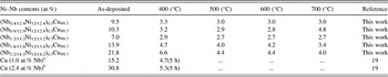
The electrical resistivities obtained in this study, together with those of Cu(Nb) films from the literature,Reference Tian and Liu18 are shown in Table I.
Electrical resistivity values in μΩ cm of Nb- and Nb–Ni-alloyed Cu films annealed for 1 h at different temperatures.

a The silicon wafers were oxidized to form a 10-nm SiO2 layer. The film thickness was about 560 nm.
b The silicon wafers were oxidized to form a 10-nm SiO2 layer. The film thickness was about 410 nm.
As shown in Table I, the resistivity values in the as-deposited condition are relatively high, which decrease after annealing. This decrease may be attributed to grain growth, defect annihilation, and stress relief in the films.Reference Chu, Lin and John2 The resistivity values reached the lowest after the 500 °C/1 h annealing, and they remained basically unchanged as the temperature increases to 600 °C. When the temperature was raised to 700 °C, the resistivity remained low for (Nb0.4/12.4Ni12/12.4)0.3Cu99.7, about 3 μΩ cm, but increased dramatically for (Nb0.9/12.9Ni12/12.9)0.3Cu99.7, from 2.8 to 4.8 μΩ cm, which might be contributed to the formation of copper silicide. The resistivities of (Nb1.8/13.8Ni12/13.8)0.3Cu99.7 and (Nb2.2/14.2Ni12/14.2)0.3Cu99.7 continuously decrease as the annealing temperature increases.
Specifically, the film (Nb1.2/13.2Ni12/13.2)0.3Cu99.7 always shows the lowest resistivities at the as-deposited condition and after annealing for 1 h at different temperatures, typically 2.7 μΩ cm, which is much lower than those of Cu (1.0 at.% Nb) and Cu (2.4 at.% Nb) films, respectively 4.7 and 5.4 μΩ cm after annealing for 5 h at 400 °C.Reference Barmak, Gungor, Cabral and Harper19
Regarding the resistivity change induced by the Ni alloying in Cu, it was shown that for every 1 at.% Ni added, the resistivity of the Cu bulk accordingly increased by 1.25 μΩ cmReference Barmak, Cabral, Harper and Rodbell20 (pure Cu as of 1.7 μΩ cm). Consequently, the Ni alloying into Cu films cannot guarantee good thermal stability as well as low resistivity.
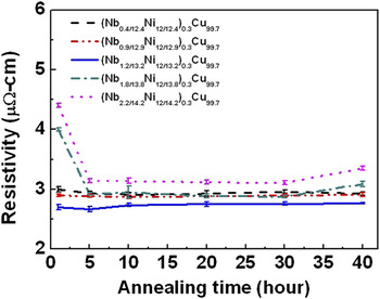
The superior diffusion barrier property of the Cu–Ni–Nb films is further confirmed by a long-term annealing for 40 h at 500 °C. The resistivity evolution of the Cu–Ni–Nb films as a function of annealing time is shown in Fig. 2. Except for a decrease in resistivity for the Nb-excessive (Nb1.8/13.8Ni12/13.8)0.3Cu99.7 and (Nb2.2/14.2Ni12/14.2)0.3Cu99.7 films at the early stage of the annealing, probably due to the precipitation of Nb that decreases the solute contents in the Cu solid solutions, the resistivities of all the others films remain basically unchanged after each annealing cycle, which indicates that the films all show high thermal stabilities. This result further confirms that the codoping of Ni and Nb contributes jointly to the stability of the alloyed Cu films. After the long annealing at 500 °C for 40 h, the resistivity of the (Nb1.2/13.2Ni12/13.2)0.3Cu99.7 film was only 2.8 μΩ cm. Also the films were all well-adhered to the substrate, even after the long annealing.
Resistivity evolution of the Cu–Ni–Nb films versus annealing time.

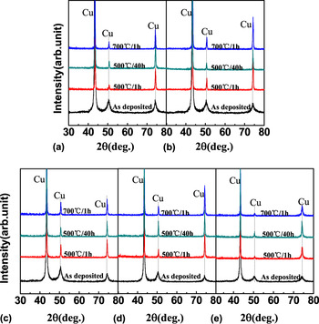
The XRD patterns in Fig. 3 show no diffraction peaks of copper silicide in all the films at both the as-deposited and the annealed states. Specifically, after annealing at 700 °C for 1 h, there are still not any extra diffraction peaks. The small amount of Cu3Si formed is surely out of the detection capability by XRD. At the same time, the peak width after annealing is narrowed in comparison with those of the as-deposited, which indicates significant grain growth and defect annihilation. Moreover, the (220) diffraction peak of the annealed samples is significantly enhanced, which shows that the doping of the Nb element changes the original [110] textured microstructure of the Cu films. According to the literature,Reference Dong, Wang, Qiang, Wang, Jiang, Han, Li, Wu and Xia15 in the Cu–Ni–Mo films, for the Ni/Mo ratios larger than 12:1, Cu3Si appeared easily after annealing. Therefore, it seems that the thermal stabilities of the present Cu–Ni–Nb films are higher than those of the Cu–Ni–Mo films.
XRD patterns of the Cu–Ni–Nb films in the as-deposited and annealed states (500 °C/1 h, 500 °C/40 h, and 700 °C/1 h) of compositions (Nb0.4/12.4Ni12/12.4)0.3Cu99.7 (a), (Nb0.9/12.9Ni12/12.9)0.3Cu99.7 (b), (Nb1.2/13.2Ni12/13.2)0.3Cu99.7 (c), (Nb1.8/13.8Ni12/13.8)0.3Cu99.7 (d), and (Nb2.2/14.2Ni12/14.2)0.3Cu99.7 (e).

To gain further insights into the microstructure evidence of the resistivity variations, the sample (Nb1.2/13.2Ni12/13.2)0.3Cu99.7 possessing the lowest resistivity was examined by TEM.
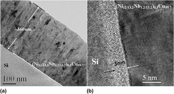
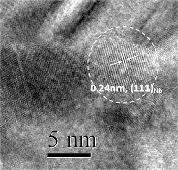
In the cross-sectional TEM image of the (Nb1.2/13.2Ni12/13.2)0.3Cu99.7 film in as-deposited state [Fig. 4(a)], a columnar structure is seen, which is typical for magnetron-sputtered thin films. The film/substrate interface is smooth and the film is well adhered to the substrate without any interfacial voids. The film has a uniform thickness of about 360 nm. The HRTEM image taken on the Cu/Si interface [Fig. 4(b)] shows that there exists a thin white layer of about 3 nm in thickness between the Cu film and the Si substrate, which is the native SiO2 layer on the initial Si wafer. This layer only has a limited diffusion inhibiting effect.Reference Shacham-Diamand, Dedhia, Hoffstetter and Oldham21Figure 5 shows the cross-sectional HRTEM image of the as-deposited film, where some Nb grains of about 5 nm in size can be found in the Cu matrix, which is owing to the slight excess of Nb. However, no Nb diffraction peak is observable in the XRD pattern due to its trace amount.
Cross-sectional TEM image of the as-deposited film (Nb1.2/13.2Ni12/13.2)0.3Cu99.7: cross-section (a) and HRTEM (b) image at the Cu/Si interface.

Cross-sectional HRTEM image of the as-deposited film (Nb1.2/13.2Ni12/13.2)0.3Cu99.7.

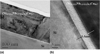
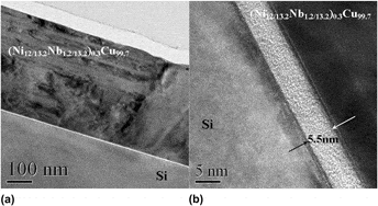
As reported in the literature,Reference Li, Liu, Zhang, Chu, Wang and Dong16 in the 400 °C/1 h-annealed pure Cu film, Cu3Si is formed on the Si substrate, and the film/substrate interface is not flat. So the formation of Cu3Si can be viewed as a sign of Cu diffusion into Si. Whereas in our 500 °C/40 h-annealed sample, the film/substrate interface remains smooth, the columnar morphology is absent, and no copper silicide is found along the film/substrate interface [Fig. 6(a)]. This means that Cu diffusion does not appear in the (Nb1.2/13.2Ni12/13.2)0.3Cu99.7 film even after the 500 °C/40 h annealing, demonstrating its application potential in Cu interconnection. The columnar crystals grow into equiaxed grains after annealing, which contributes to the decrease of the resistivity. However, it is reported that after a 400 °C/5 h annealing, the grains grew up to 50 nm from 21 nm for a Cu (1.0 at.% Nb) film and to 50 nm from 42 nm for a Cu (2.4 at.% Nb) film,Reference Barmak, Cabral, Harper and Rodbell20 that is to say, no significant grain growth occurred in these films, which is much different from the present Nb–Ni coalloyed Cu films. Figure 6(b) shows a cross-sectional HRTEM image of the Cu/Si interface in the annealed film, where the thickness of a native SiO2 layer is 5.5 nm, which is 2.5 nm thicker than that in the as-deposited film, possibly due to the diffusion of residual O2 in the vacuum chamber through the film to the interface.
Cross-sectional (a) and high-resolution (b) TEM images of the 500 °C/40 h-annealed film (Nb1.2/13.2Ni12/13.2)0.3Cu99.7 taken at the Cu/Si interface.

Actually, the Cu–Ni–Nb films can be evaluated from two aspects. On the one hand, the resistivity of the film should be low enough, as close as possible to the resistivity of pure Cu film. On the other hand, the thermal stability of the film should be high enough so that the resistivity remains stable after annealing at 500 °C for 40 h to satisfy the practical process requirements of integrated circuit. Viewing these aspects, the (Nb1.2/13.2Ni12/13.2)0.3Cu99.7 film is the best for its lowest resistivity and highest stability.
IV. CONCLUSIONS
A series of Cu–Ni–Nb ternary films were prepared on Si wafer substrates by magnetron cosputtering of pure Cu targets glued with Ni–Nb alloys of different Ni/Nb ratios. The codoping of minor amounts of Ni and Nb, about 0.3 at.%, contributes significantly to the high thermal stabilities and the low resistivities. All the samples showed no detectable copper silicide in XRD patterns even after annealing at 700 °C for 1 h and at 500 °C for 40 h. In particular, after annealing at 500 °C for 1 h, the (Nb1.2/13.2Ni12/13.2)0.3Cu99.7 film, with a Ni/Nb ratio close to 12/1, showed the lowest resistivity of about 2.7 μΩ cm, and after 40 h annealing at 500 °C, it maintained a low resistivity of about 2.8 μΩ cm.
ACKNOWLEDGMENT
This project was supported by the National Science Foundation of China (Grant Nos. 51271045 and 11174044).