Introduction
Transparent conducting oxides (TCO) have attracted considerable interest as materials because of their important role as contacts and active elements in transparent thin-film transistors, organic light-emitting diodes, flexible displays, and solar cells.[ Reference Ko, Kim, Kim, Cho, Park and Choi 1 – Reference Ginley, Coutts, Perkins, Young, Li and Parilla 3 ] Historically, polycrystalline tin-doped In2O3 (ITO) has been one of the preeminent materials for transparent contacts due to its good electrical and optical properties. However for many applications, the limitations of ITO, including its low work function, high processing temperature, rough surface, and chemical incompatibility may limit its utility. Other binary TCO materials, such as fluorinated SnO2 (FTO), and Al- or Ga-doped ZnO (AZO, GZO)[ Reference Fortunato, Ginley, Hosono and Paine 4 , Reference Sigdel, Ndione, Perkins, Gennett, van Hest, Shaheen, Ginley and Berry 5 ] have some desirable properties, but do not meet all the criteria for many emerging applications, leading to an increasing search for new materials.
These limitations have created an increased interest in ternary materials, such as indium zinc tin oxide (IZTO), as promising candidates for ITO substitutes.[ Reference Marks, Veinot, Cui, Yan, Wang, Edleman, Ni, Huang, Lee and Armstrong 6 , Reference Proffit, Philippe, Emery, Ma, Buchholz, Voorhees, Bedzyk, Chang and Mason 7 ] In particular, the fabrication of amorphous IZTO (a-IZTO) thin films is of increasing interest. Foremost, amorphous materials are deposited at lower temperatures than their crystalline counterparts. This simplifies deposition/manufacturing processes and expands the range of compatible substrates upon which the material can be deposited, such as plastics, potentially reducing cost and improving throughput. Amorphous materials tend to be less susceptible to fracture and hence are useful in applications requiring flexibility, i.e. flexible optoelectronics.[ Reference Kim, Hwang, Eun and Choa 8 – Reference Kumar, Sigdel, Gennett, Berry, Perkins, Ginley and Packard 11 ] a-IZTO could also exhibit much reduced surface roughness and higher thermal stability than a-ITO, since the transition from amorphous to crystalline has been demonstrated to occur at higher temperature.[ Reference Proffit, Philippe, Emery, Ma, Buchholz, Voorhees, Bedzyk, Chang and Mason 7 , Reference Son, Ko, Jung, Boo, Choa and Kim 12 ] In addition, it has been shown that IZTO exhibits higher work function than ITO, which can be important in minimizing band alignment mismatching in some applications.[ Reference Marks, Veinot, Cui, Yan, Wang, Edleman, Ni, Huang, Lee and Armstrong 6 ]
To facilitate the move of IZTO thin films into practical applications, it is very important to be able to control their morphology and opto-electronic characteristics. The primary requirements for TCOs are high electronic conductivity and good visible transparency. The secondary requirements are process environment, chemical stability, interfacial properties; also good mechanical properties are necessary for manufacturing, durability, and flexibility. In this sense, IZTO is attracting a lot of interest since first reported by Phillips et al.[ Reference Phillips, Cava, Thomas, Carter, Kwo, Siegrist, Krajewski, Marshall, Peck and Rapkine 13 ], but the majority of experimental work varying the cation composition of IZTO has focused on a small portion of the ternary phase diagram. Subsolidus phase relationships on a wider range of composition at high temperature (1275 °C) have been established for crystalline IZTO by Harvey et al.[ Reference Harvey, Poeppelmeier and Mason 14 ] but such broad compositional information is not available for the amorphous material. Combinatorial methods have been used to study properties of In-poor IZTO[ Reference Ryu, Yang, Park, Hwang and Jeong 15 ] and related IGZO[ Reference Iwasaki, Itagaki, Den, Kumomi, Nomura, Kamiya and Hosono 16 ] thin films as a function of composition, both for amorphous oxide semiconductor transistor applications, similar to the related IZO compound.[ Reference Taylor, Readey, Teplin, Hest, Alleman, Dabney, Gedvilas, Keyes, To, Perkins and Ginley 17 ]
In this study, we investigate the properties of a-IZTO thin films fabricated by combinatorial RF magnetron co-sputtering at room temperature. By broadly varying the cationic composition with several fixed deposition parameters such as gas pressure, we were able to determine the effect of cation composition on the structural, mechanical, electrical, optical, and surface properties of IZTO. Based on the values of the electrical conductivity, the depositions conditions were optimized by using argon (without oxygen) at partial pressure of 10 mTorr. The results of our high-throughput study based on more than 1500 different cationic compositions of IZTO from combinatorial libraries show that the electrical conductivity varies with chemical composition, such that the most conductive thin films have high In content. No structural variation as a function of composition is observed by X-ray diffraction (XRD) for the a-IZTO films. The composition also has a very little influence on the optical absorption onset. Mechanical properties show that a-IZTO is a durable material that could be used in flexible electronic devices. Overall, our findings provide guidance on how to optimize multiple properties simultaneously and enable control of the physical properties of IZTO for practical applications.
Experimental
The IZTO combinatorial libraries were deposited onto stationary 2 × 2″ glass substrates at room temperature by combinatorial radiofrequency (RF) magnetron co-sputtering.[ Reference Bunn, Voepel, Wang, Gatzke, Lauterbach and Hattrick-Simpers 18 ] For a fine tuning of the cation composition, the depositions were performed from three different ceramic targets of pure (99.9%) In2O3, SnO2, and ZnO. The system was evacuated to a base pressure < 2 × 10⁻⁶ mTorr using a cryogenic pump. The substrate-to-target was maintained at 10 cm. The RF power for the In2O3 and SnO2 targets was varied between 20 and 65 W and the power for the ZnO target was 100 W. The deposition time varied from 20 to 30 min. Each of the combinatorial libraries was automatically mapped at 44 points (4 × 11 grid) to find the properties of the material as a function of off-stoichiometry. The samples were routinely measured using X-ray fluorescence (XRF), XRD, optical spectroscopy, four-point probe sheet resistance mapping, Kelvin-probe (KP) mapping, and nanoindentation. All measurements were indexed to probe the same points. These spatially resolved characterization results were analyzed using custom routines written in Igor Pro software package. More information about the combinatorial approach in general[ Reference Green, Takeuchi and Hattrick-Simpers 19 ] and about our implementation of it[ Reference Zakutayev, Perkins, Parilla, Widjonarko, Sigdel, Berry and Ginley 20 ] can be found in published literature.
XRF spectra were collected using Roentgenanalytic maXXi 5/PIN instrument and analyzed using MTF-FP software to obtain both chemical composition and thickness of the samples (200 ± 50 nm) confirmed by spectroscopic ellipsometry (M-2000, Woollam). XRD patterns of Cu K α radiation were collected using a Bruker D8 instrument with a proportional two-dimensional detector. The KP measurements were performed on the KP Technologies instrument using a gold tip and aluminum/gold references. The optical measurements were performed on a custom transmittance/reflectance fiber optics-based setup with an array of Ocean Optics detectors. The absorption spectrum (Supplementary Fig. S3) for each composition was calculated from the corresponding transmittance (T) and reflectance (R) values using the following expression:
 $$T = (1 - R)e^{( - \alpha d)}$$
with α being the absorption coefficient and d being the film thickness. The sheet resistance was measured using collinear four-point probe technique using Signatone tungsten probe tips on a custom instrument. The absorption onset was obtained by extrapolating the linear region of the absorption coefficient spectra (plotted as a function of hν) to zero absorption (α = 0).
The mechanical properties, including reduced modulus and hardness, of several In–Zn–Sn–O combinatorial libraries were measured at all 44 locations. The reduced modulus, E r, is given as
 $$\displaystyle{1 \over {E_{\rm r}}} = \displaystyle{{1 - \nu _{{\rm sample}}^2} \over {E_{{\rm sample}}}} + \displaystyle{{1 - \nu _{{\rm tip}}^2} \over {E_{{\rm tip}}}},$$
where E and ν are the elastic moduli and Poisson's ratios of the sample and indenter tip, respectively. It was measured using a Hysitron TI 950 Triboindenter (Minneapolis, USA) equipped with nanoDMA III. At each of the 44 locations representing a single composition, four indentations separated by 20 µm were performed. Dynamic indentations were performed in the CMX mode with in situ drift correction.[ Reference Li and Bhushan 21 ] The dynamic testing was performed at 220 Hz, loading at a constant strain rate of 0.126 s−1 up to a peak force of 700 µN. Depth-dependent modulus and hardness data were collected during the entire dynamic segment of each test and averaged for each composition. Analysis was restricted to data acquired from within the first 5%–10% of the total film thickness to minimize influence from the substrate.
Results and discussion
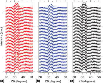
All IZTO films were amorphous by XRD, regardless of the deposition conditions (Fig. 1 and Supplementary Fig. S1). This conclusion is supported by the normal and grazing XRD data that show only a broad and weak peak, consistent with an a-IZTO material. The lack of long ranges order in amorphous structure leads to an extremely low number of grain boundaries and consequently a reduced importance of mechanical and electrical effects in those grain boundaries. Therefore, the films are expected to have mobilities as good or better than crystalline samples. The reason is that for certain ionic materials, such as the main-group oxides studied here, grain boundaries in crystalline samples often cause a reduction in the mobility due to increased scattering of carriers.[ Reference Buchholz, Proffit, Wisser, Mason and Chang 22 ] It also has been shown that such high mobility exhibited by amorphous oxides originates from the fact that large spherical s orbitals form electron transport paths, and the strong ionic bonds do not form high electron density traps in the band gap.[ Reference Kamiya, Nomura and Hosono 23 ]
XRD scans of IZTO thin-film libraries with different cation compositions deposited at P T = 10 mTorr (Ar only). (a) 76% ≤ In ≤89% (including In0.87Zn0.07Sn0.06O y ), (b) 43% ≤composition range of In ≤55% (including In0.52Zn0.38Sn0.15O y ), (c) 7% ≤ In ≤21% (including In0.08Zn0.41Sn0.51O y ). Each plot corresponds to a library (scan of 44 points on one 2 × 2″ glass substrate corresponding to 44 different compositions).

First, we deposited the a-IZTO thin films at different deposition conditions and measured their electrical properties. The electrical conductivity results were very sensitive to both the total pressure (P T) and the oxygen (P O2) partial pressure. Although P T and P O2 was varied through a wide values range, there were deposition parameter thresholds for detecting a minimum conductivity in the IZTO films, within the resolution limit of our four-points measurement setup. The maximum total pressure P T = P O2 + P Ar and gas ratio (P O2/P Ar) for a threshold of a measured conductivity value are P T = 20 mTorr and P O2/P Ar = 0.001, respectively. The conductivity results for these deposition conditions are shown in Supplementary Fig. S2. The highest conductivity values were measured at optimum deposition pressure of P T = 10 mTorr without oxygen (P T = P Ar). Therefore the deposition was kept at this P T for the combinatorial study of the phase diagram of IZTO as a function of conductivity, absorption onset and work function, screening more than 1500 different cationic compositions of IZTO.
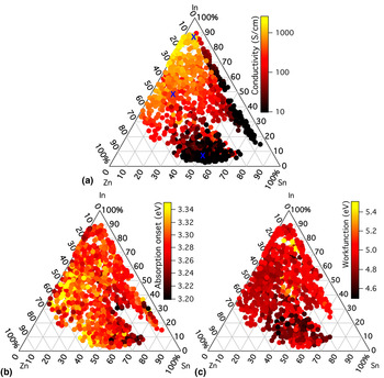
Second, we consider the electrical conductivity of a-IZTO films as a function of cation composition. The maximum conductivity of 2415 S/cm is reached when the In/Zn and In/Sn is in the range of 0.60–0.88 and 0.80–0.88, respectively, as shown in Fig. 2(a) (see also Supplementary Fig. S1). This conductivity value is comparable with the one measured on crystalline ITO films. The three compositions indicated with blue crosses in Fig. 2(a) and reported in Table 1 give the range of tunability from as good or better than ITO to near insulating with transmittance over 85%. To evaluate the origin of the changes in conductivity, IZTO films with different compositions (single composition with the absence of gradient for each sample) were fabricated and their electronic properties evaluated with Hall measurements. Values of mobility and carrier concentration for the different film compositions are presented in Table 1. It is found that the change in conductivity is mainly influenced by the changing carrier concentration rather than the varying mobility.
Properties of a-IZTO thin films deposited at P T = P Ar = 10 mTorr with different compositions: (a) conductivity with σ ≈ 10–2415 S/cm (blue crosses indicate compositions chosen for Hall measurements), (b) absorption onset with α ≈ 3.15–3.35 eV, and (c), work function with φ ≈ 4.5–5.6 eV. Note that the missing compositions for the work function (when compared with the absorption and the conductivity) in the ternary diagram are related to samples from which reliable work function data could not be obtained due to their high resistivity.

Carrier concentration and mobilities (measured by Hall), conductivity (determined by four-point probes), absorption coefficient (determined from transmission and reflection measurements), and work function (measured by Kelvin probe) for three different compositions [indicated with blue crosses in Fig. 2(a)].

Both oxygen gas pressure and cation content play a role on conductivity of a-IZTO thin films. It is also clear that the IZTO films become more resistive at both high Sn/In ratio and low Zn/In ratio. In particular, the lowest conductivity is observed at the highest Sn/In ratio rather than the highest Zn/In ratio, which is chemically non-intuitive since Sn (and not Zn) usually acts as a dopant in crystalline In2O3.[ Reference Rosen and Warschkow 24 ] The decrease of conductivity with the increase of Sn in the films is most likely due to the fact that Sn does not act as independent dopant in IZTO and the presence of Zn may act as compensating acceptor defects to the Sn donor dopants. In this case, Sn acts as an electron trap rather than an electron donor in IZTO, with the formation of donor acceptor pairs from Zn2+ and Sn4+, which would prevent carrier generation.[ Reference Palmer, Poeppelmeier and Mason 25 ] In fact, as reported by Lu et al.[ Reference Lu, Yang, Ling, Cong, Zhang, Li and Xin 26 ] the solubility of Zn/Sn dopants are both promoted in IZTO more than SnIn or ZnIn defects in In2O3 because of the isovalent substitution of Sn4+ and Zn2+ for two In3+. The existence of ZnIn is beneficial to the donor defects favorable to the increase of carrier concentration in IZTO.
The high conductivity at high In content in the film indicates the presence of a charge-carrier source related to In. It is often claimed that the main source of conductivity in undoped crystalline In2O3 are bulk oxygen vacancies that act as a charge-carrier source.[ Reference González 27 ] An alternative explanation is the oxygen vacancy or indium interstitial defects located at the surface.[ Reference Frank and Köstlin 28 ] Regardless of their configuration and location, these donors would be formed by removing some of the bulk- or surface oxygen anions under reducing conditions (like in our case where the optimal deposition conditions are under 10 mTorr of Ar gas with no oxygen gas). Another possible explanation is related to Zn and Sn atoms. From the theoretical point of view, it is known that Zn serves as a dopant to compensate Sn elements and bind oxygen vacancies in crystalline IZTO, leading to higher doping level, better charge transport ability, and consequently to higher conductivity.[ Reference Lu, Yang, Ling, Cong, Zhang, Li and Xin 26 ] In the case of our amorphous films, the role of both Zn and Sn are less clear, although experimental results (Fig. 2, see also Supplementary Fig. S2) strongly indicate that increasing both the Zn/In and Sn/In ratio dramatically influence the electrical properties. So altogether, one may suggest that the conductivity in the IZTO films may be affect by both cation substitutions (Sn and Zn) and In2O3-related donor defects (originated from depositions with crystalline In2O3 target and under reducing conditions), since both can act as carrier donors in amorphous oxides.
Next, we turn our attention to optical properties of IZTO, which is the other important TCO metric besides the electrical conductivity. The absorption onset of a-IZTO thin films as a function of composition has been determined from the transmittance and reflectance measurements, and the results are shown in Fig. 2(b) (see also Supplementary Fig. S4). The average transmittance over the visible wavelength range (400–800 nm) was higher than 85% for a-IZTO films thickness of about 230 nm, which compares well with the values measured for crystalline ITO films. The absorption onset of the IZTO films varied from 3.20 to 3.34 eV with an optimum highest value obtained for a-IZTO films deposited at P T = 10 mTorr. Although the slightly higher absorption onset is found at IZTO composition with Zn ratio varying between 50% and 70% and Sn ratio varying between 10% and 40%, the cation composition does not have a significant impact on the optical properties of the films. Based on the Burnstein–Moss theory, a degenerate semiconductor should exhibit an increase of band gap with increasing carrier concentration. However, for our films, there is no evidence of the absorption onset increase with increasing carrier concentration up to mid-1020 cm−3 values (Table 1). Therefore, the hypothesis of degenerate semiconductor behavior can be excluded in this study.
For certain applications, such as electrical contacts in solar cells and light-emitting diodes, the surface properties of the TCO material are as important as the optical transparency and electrical conductivity discussed above. From this point of view, the work function (φ) results for our a-IZTO thin films are reported in Fig. 2(c) (see also Supplementary Fig. S5). The a-IZTO work function varies from 4.6 to 5.3 eV and tends to increase with increasing Sn and In content. The lowest work function is measured at IZTO compositions with over 50% of Zn and 30% In content. Also, IZTO films grown under oxygen atmosphere, exhibit higher work function than the films grown under argon atmosphere (see Supplementary information). Overall, these values of work functions are consistent with what has been reported into the literature for the related materials.[ Reference Son, Ko, Jung, Boo, Choa and Kim 12 , Reference Lee, Ji, Park, Tark, Park, Lee, Kim, Kang, Lee and Kim 29 ]
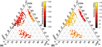
Finally, we evaluate the mechanical properties of the IZTO films, to assess their potential applications in flexible electronics. The reduced modulus and hardness measured with dynamic indentations are shown in Fig. 3. The variation of mechanical properties with different cation composition is clearly visible. The reduced modulus varies by 7%–12% [standard deviation (SD) ≈ 5%] and does not show any strong dependence on the composition, while the hardness varies by 15%–25% (standard deviation ≈ 5%), with highest values for low tin content over a wide range of In and Zn incorporation. In terms of absolute numbers, reduced modulus varies between 120 and 145 GPa, while the hardness varies from 10 to 14 GPa for the a-IZTO thin films reported here.
(a) Reduced modulus and (b) hardness of IZTO thin film with different cation compositions.

Measurement of elastic modulus is highly sensitive to porosity; thus we compare the range of measured reduced elastic moduli from our amorphous films with the range of elastic moduli reported for crystalline end-member oxides and data from the limited surveys of thin-film polycrystalline oxides. The Young's modulus for tin oxide bulk material is reported to be 174–368 GPa (depending on surface orientation).[ Reference Li and Bradt 30 , Reference Barth, Harnagea, Mathur and Rosei 31 ] The Young's moduli reported for zinc oxide thin films were in the range of 120–140 GPa.[ Reference Mukhopadhyay, Chaudhuri, Seal, Dalui, Banerjee and Phani 32 , Reference Martin, Dadon, Rosen, Gershon, Birman, Levush and Carmel 33 ] For polycrystalline tin-doped indium oxide in thin-film form, an average elastic modulus of 189 GPa has been measured in one study, and is among the highest values reported.[ Reference Pradeepkumar, Sibin, Swain, Sridhara, Dey, Barshilia and Sharma 34 ] For comparison, in most of the studies the Young's modulus is reported to be 99–120 GPa for tin-doped indium oxide.[ Reference Zeng, Zhu, Hu, Shen, Zhang and Gong 9 , Reference Ashida, Miyamura, Oka, Sato, Yagi, Taketoshi, Baba and Shigesato 35 ] Our range of reduced modulus, from 120 to 145 GPa compares well with literature values for crystalline material, thus we conclude that the films deposited here are fairly dense, consistent with the relatively high carrier mobilities.
The hardness of the films is relevant to film strength, durability during handling, and potentially wear resistance in applications where the coating is exposed[ Reference Kumar, Sigdel, Gennett, Berry, Perkins, Ginley and Packard 11 , Reference Ginley, Hosono and Paine 36 , Reference Cairns, Paine and Crawford 37 ]. For comparison, the hardness of ITO is reported to be 6.5 GPa[ Reference Zeng, Zhu, Hu, Shen, Zhang and Gong 9 ]. The hardness values of all IZTO films measured here (10–14 GPa) exceed that of ITO. The increase of hardness is a reflection of increased strength, which is supported by an earlier report that IZTO films have higher resistance to failure in bending[ Reference Kim, Hwang, Eun and Choa 8 ]. Additionally, the hardness of all measured films is equal to or greater than that of glass[ Reference Gordon 38 ], providing evidence of mechanical durability and utility even where the TCO is exposed to the environmental conditions.
Conclusions
High-throughput experimental methods, including combinatorial synthesis and spatially resolved characterizations, have been applied to IZTO thin films. The IZTO films grown at room temperature by RF sputtering showed an amorphous-like phase and optical transmittance >85% in the visible region, regardless of the cation composition and the deposition pressure. Optimized conditions were obtained by using 10 mTorr argon partial pressure, since the use of oxygen partial pressure leaded to a dramatic decrease in conductivity of the films. Conductivity and work function were both influenced by the a-IZTO composition. Additionally, a-IZTO is a durable material, with sufficiently high mechanical properties across a wide range of compositions. In summary, the results of our study determine ways of tuning the properties of a-IZTO thin films by changing the cation composition and deposition conditions. This work shows that a-IZTO films deposited at room temperature may serve as a viable, low-cost alternative to conventional polycrystalline ITO films. In the future, a-IZTO films may be used as transparent electrodes in electrical contacts for thin film solar cells, such as front contact in Cu(In,Ga)Se2 or back contact in CdTe.
Supplementary material
The supplementary material for this article can be found at https://doi.org/10.1557/mrc.2016.57
Acknowledgment
This work was supported by the U.S. Department of Energy, under Award Number DE-AC36-08GO28308 to the National Renewable Energy Laboratory (NREL). P.F.N. and A.Z. gratefully acknowledge support from the U.S. Department of Energy, Office of Science, Basic Energy Sciences Program, as part of the CNMGD Energy Frontier Research Center. J.D.P. and D.S.G. gratefully acknowledge support from Office of Energy Efficiency and Renewable Energy, Solar Energy Technology Program, as a part of SunShot initiative. M.K. gratefully acknowledges funding from Center for Revolutionary Solar Photoconversion (CRSP). C.P. gratefully acknowledges funding from a joint appointment at NREL. P.F.N. would like to thank Dr. Thomas Gennett and Dr. Philip Parilla at NREL for useful discussions.