Introduction
Numerous applications require thermally robust metal thin films that possess both high strength and corrosion resistance. Examples of high-temperature applications include thermal inkjet printing,[Reference Allen, Meyer and Knight1] pressure sensors in combustion engines,[Reference Fonseca, English, von Arx and Allen2] and turbine blade protective coatings.[Reference Goward3] Semiconductor manufacturing also requires thermal stability of metals to 400 °C for back-end-of-line processing[Reference Farcy, Carpentier, Thomas, Torres and Ancey4] and above 1000 °C for gate metal annealing.[Reference Wolf and Tauber5]
An amorphous metal thin film (AMTF) is an attractive option for such applications. It lacks the grain boundaries and dislocations of crystalline materials, which degrade mechanical strength and provide pathways for chemical attack. Additionally, an amorphous thin film possesses an ultra-smooth surface when deposited onto a substrate with a smooth surface, a feature that often enhances device performance. These attributes have stimulated interest in their use for many emerging applications.[Reference Chu, Jang, Juang, Chou, Yang, Yi, Wang, Lee, Liu, Liaw, Chen, Lee, Li and Rullyani6, Reference Kumar, Desai and Schroers7]
Amorphous metals are metastable and prone to crystallize at high temperatures. Once crystallized, their performance advantages are lost. We examine here how to produce new refractory amorphous thin films with high crystallization and oxidation temperatures.
Amorphous metals comprising refractory elements, such as Ta, W, or both, are expected to crystallize at high temperatures, since the crystallization temperature of an amorphous metal depends on the melting point of its constituent elements.[Reference Zhang, Ma and Xu8] Compositions with metalloids, such as Si, further enhance high-temperature stability. The metalloid contributes to large negative heats of mixing, increases atomic-size diversity, and forms strong bonds with the refractory metals, all factors that increase the high-temperature stability of the amorphous structure.[Reference Suryanarayana and Inoue9, Reference Takeuchi and Inoue10] Refractory amorphous alloys that employ these features have crystallization temperatures ranging from 800 to over 1100 °C.[Reference Grubbs, Zhang, Deal, Nishi and Clemens11–Reference McGlone, Olsen, Stickle, Abbott, Pugliese, Long, Keszler and Wager14]
We describe herein the properties of three new refractory AMTFs derived from the target compositions Ta40W40Si20, Ta30W50Si20, and Ta30W30Si40. These compositions were chosen to systematically examine the effects of both refractory metal and metalloid content across a narrow range to suppress crystallization. The structures, electrical properties, and thermal stabilities of these films are compared with those of sputtered Ta thin films.
Experimental
Dense 2-in. metal targets of nominal composition Ta40W40Si20, Ta30W50Si20, and Ta30W30Si40 were purchased from Materion. Thin films were deposited by magnetron sputtering onto 25-mm2 Si/SiO2 substrates at a base pressure <10−6 Torr. Thin films were sputtered at 100 W RF power and sputtering pressures from 5 to 20 mTorr. The substrate to target throw distance was set to 4 in. and no substrate bias, cooling, or heating were applied. Ta40W40Si20, Ta30W50Si20, and Ta30W30Si40 thin films were sputtered at rates near 7, 10, and 8 nm/min, respectively, to a thickness of approximately 200 nm, which was confirmed with an Alpha-Step 500 Surface Profilometer. Unless stated otherwise, measurements were made on the 200-nm-thick films. Resistivity was assessed from film thickness and resistance measured with a Jandel RM-2 collinear four-point probe.
Transmission electron microscopy (TEM) and convergent beam electron diffraction (CBED) experiments were performed with a FEI Titan 80-200 TEM/STEM. TEM samples were first coated with amorphous carbon (a-C) and chromium before being sectioned for analysis. CBED analysis was performed with a converged beam size of 50–200 nm2. Surface roughness and morphology were determined by atomic-force microscopy (AFM) with an Asylum atomic-force microscope operating in contact mode. Scanning electron microscope (SEM) images were acquired with an FEI Helios 650 dual beam SEM operating in immersion mode with a circular backscatter detector.
Crystallization temperatures were measured after heating samples in evacuated (20–50 mTorr), sealed fused-silica tubes, at selected temperatures between 800 and 1100 °C. The tubes were heated at 5 °C/min with 20-min dwell at the final temperature. Grazing-incidence x-ray diffraction (GI-XRD) data were acquired with a Rigaku Ultima-IV x-ray diffractometer equipped with a thin-film stage.
Film compositions were determined by electron probe microanalysis (EPMA) with a Cameca SX100 electron probe micro-analyzer. Films were deposited on Cu substrates for analysis.
X-ray photoelectron spectroscopy (XPS) measurements were made with a PHI Quantera Scanning ESCA spectrometer equipped with a monochromatic Al x-ray source having a photon energy of 1486.6 eV. The data were charge-corrected to carbon 1s at 284.8 eV. The binding energy (BE) scale was calibrated with the Cu 2p 3/2 feature at 932.7 ± 0.05 eV and Au 4f at 84.0 ± 0.05 eV. Compositions were determined by using standard elemental relative sensitivity factors corrected for the transmission function of the analyzer. Sputter depth profiles were acquired by alternately sputtering and acquiring spectral data. Samples were sputtered with a 2-kV Ar+ ion beam at a sputter rate of ~5 nm/min relative to SiO2. The sputter depth-profile data were reduced by using a linear least-squares method to separate overlap of the Ta 4f and the O 2s signals and to assign the chemical state of silicon to silicide or oxide.[Reference Stickle, Briggs and Grant15]
Results and discussion
Structure, electrical properties, and composition
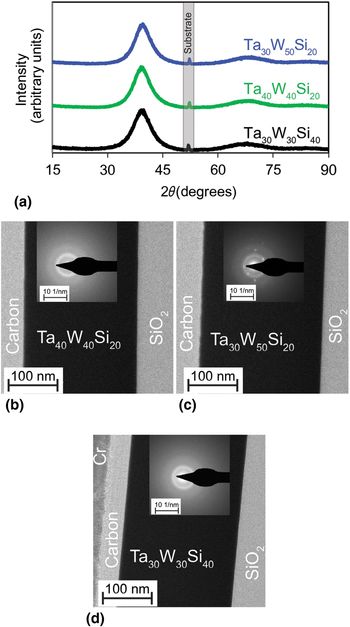
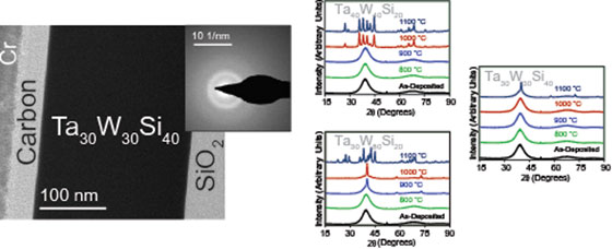
Figure 1(a) shows GI-XRD patterns for Ta40W40Si20, Ta30W50Si20, and Ta30W30Si40 thin films. The broad features from approximately 35° to 45° and 60° to 75° are indicative of an amorphous thin film. The absence of Bragg reflections, i.e., sharp, distinctive peaks, indicates a lack of long-range crystalline order. Figures 1(b), 1(c), and 1(d) show CBED patterns for the three compositions. The patterns for Ta40W40Si20 and Ta30W30Si40 exhibit diffuse halos, which confirm the amorphous character of the films. Similarly, the pattern for Ta30W50Si20 shows diffuse halos, but also sharp spots. These spots represent nanocrystalline domains of WSi2[Reference Tanaka, Nawata, Inui, Yamaguchi and Koiwa16] embedded in an environment of amorphous metal. From the high-resolution TEM image and the lack of diffraction peaks in the GI-XRD pattern, we estimate the diameter of the nanocrystallites to be <4 nm. Considering the small grain size and apparent low concentration of the crystallites, we consider the samples to be substantially amorphous.
(a) As-deposited GI-XRD patterns for thin films of Ta40W40Si20, Ta30W50Si20, and Ta30W30Si40 with the silicon substrate peak identified. TEM cross-section and convergent beam electron diffraction (CBED) pattern of a (b) Ta40W40Si20, (c) Ta30W50Si20, and (d) Ta30W30Si40 thin film. Diffraction analysis of Ta40W40Si20 and Ta30W30Si40 confirms the amorphous structure and shows no evidence of crystallinity in the thin film. Diffraction analysis of Ta30W50Si20 confirms the structure to be amorphous with a small fraction of nanocrystalline domains embedded in the amorphous structure.

Table I summarizes surface roughness, resistivity, and composition for each film as-deposited. The root-mean-square (rms) surface roughness, determined by AFM, is <0.5 nm for each film. The ultra-smooth nature of the surfaces further characterizes the films as amorphous. The room temperature resistivities are all ~200 µΩ cm, which is in the range expected for an amorphous metal. Note that the resistivity of an amorphous metal is expected to be higher than that of its constituent crystalline elements.[Reference Suryanarayana and Inoue9] Typical sputtered β-Ta, α-Ta, and W thin films possess resistivities of 165, 25, and 14 µΩ cm, respectively.[Reference Schauer and Roschy17, Reference Bouziane, Mamor and Meyer18]
Properties of as-deposited TaWSi thin films.

a Film composition estimated via EPMA, neglecting oxygen (≤5%).
The Si concentration in all of the TaWSi thin films is lower than that of the target. We find that Si is preferentially deposited off-axis onto the sputter chamber walls. Other researchers have previously reported that magnetron sputtering with a multicomponent target may result in a thin-film composition different from that of the target.[Reference Chapman19, Reference Betz, Wehner and Behrisch20] For example, sputtered WTi[Reference Shaginyan, Misina, Kadlec and Jasterbi21] and WSi[Reference Murakami and Shingyoji22] thin films exhibit a reduced concentration of the lighter element, Ti and Si, respectively, compared with that of the target. These results are consistent with the compositional trends of the films.
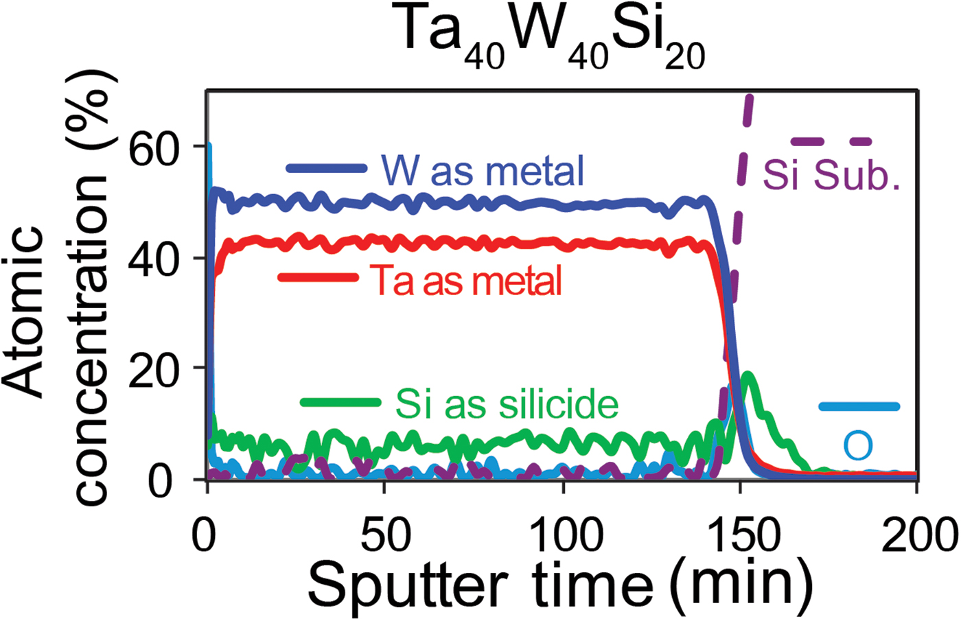
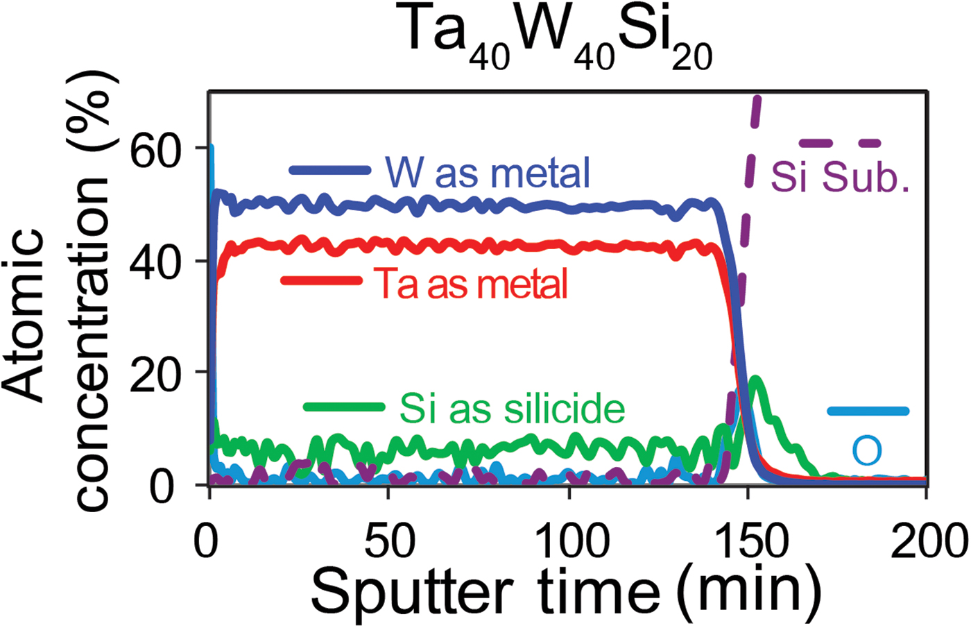
Figure 2 shows an XPS composition and chemical-state depth profile of a 200-nm-thick Ta40W40Si20 thin film. For XPS composition and chemical-state depth profiles of Ta30W50Si20 and Ta30W30Si40 thin films, see Supplementary Figs. S1(a) and S1(b), respectively. The depth profiles demonstrate that the elemental distribution of Ta, W, and Si is uniform throughout the bulk of the thin film. Note that the atomic ratios in Fig. 2 cannot be compared directly with the composition established by EPMA, as the compositional depth profile has not been corrected for preferential sputtering. The data also show that Si is present as silicide, which is also consistent with the low, observed O content.
XPS composition sputter depth profile of a Ta40W40Si20 thin film showing uniform composition throughout the bulk of the film. Atomic concentrations are not corrected for preferential sputtering.
Thermal studies
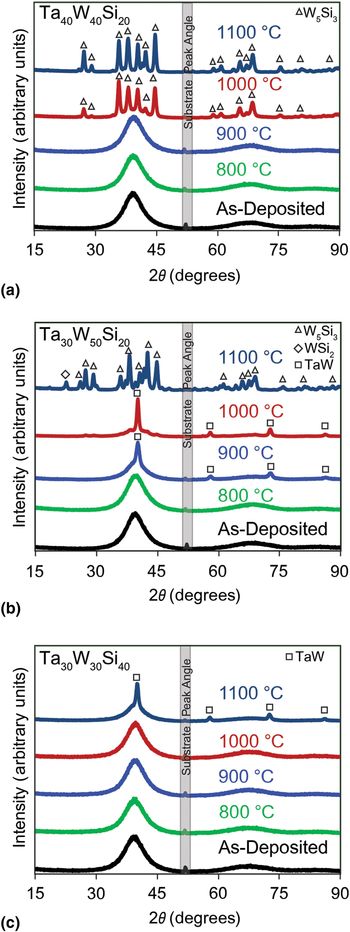
Figure 3 shows GI-XRD patterns of Ta40W40Si20, Ta30W50Si20, and Ta30W30Si40 thin films as-deposited and heated in 100 °C increments to 1100 °C in evacuated, sealed silica tubes. The broad features in the patterns of Ta40W40Si20 [Fig. 3(a)] indicate that the film remains amorphous to 900 °C. At 1000 °C, the broad features change to sharp Bragg reflections arising from crystalline material. The remaining diffuse background indicates an amorphous fraction remains at this temperature and annealing time. At 1100 °C, the amorphous contribution reduces as the Bragg intensities increase because of additional crystal growth. Phase analysis shows the crystalline material to be W5Si3 (see Supplementary Fig. S2).
XRD patterns from (a) Ta40W40Si20, (b) Ta30W50Si20, and (c) Ta30W30Si40 thin films as-deposited and after post-deposition annealing. The silicon substrate peak at ~52.5° is indicated.

Figure 3(b) shows Ta30W50Si20 to be amorphous at 800 °C. At 900 °C, a new sharp peak appears near 42°, indicating the film begins to crystallize. As the temperature increases to 1000 °C, the intensity of this peak grows, while the broad diffuse background intensity decreases. The diffraction peaks at 900 and 1000 °C are consistent with elemental W or a TaW solid solution [see Supplementary Fig. S3(a)]. After the 1100 °C anneal, the thin film undergoes additional reaction and grain growth to form a mixture of crystalline W5Si3 and WSi2 [see Supplementary Fig. S3(b)].
Figure 3(c) shows the GI-XRD patterns for Ta30W30Si40 change little up to 1000 °C; they exhibit only broad peaks consistent with an amorphous structure. At 1100 °C, sharp Bragg peaks emerge that match those of W or a WTa solid solution (see Supplementary Fig. S4). If the temperature were further increased, we expect a silicide phase to form.
To summarize, the x-ray data show crystalline W (or TaW) separates from Ta30W50Si20 above 800 °C. This W segregation is suppressed with the smaller W content in Ta40W40Si20. This material clearly crystallizes as a mixture of silicides at 1000 °C. The increased Si content of Ta30W30Si40 then suppresses both silicide and W (TaW) formation, increasing the crystallization onset to temperatures above 1000 °C. Consequently, the crystallization temperature of the Ta30W30Si40 system is similar to that of quaternary amorphous metal systems based on Ta, W, Si, and C,[Reference Grubbs, Zhang, Deal, Nishi and Clemens11, Reference Ouyang, Wongpiya, Grubbs, Deal, Clemens and Nishi12] which are among the higher reported crystallization temperatures for amorphous metals. TaWSi provides advantages under some conditions, as C commonly migrates from metals at high temperatures.
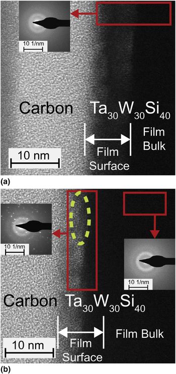
Figure 4(a) shows a TEM image and a CBED pattern for the near-surface region of the most thermally stable film composition, i.e., Ta30W30Si40, after a 1000 °C anneal. The TEM image reveals the film to be continuous and smooth. No interactions are observed between the substrate and the thin film as seen in Supplementary Fig. S5 in the supplemental section. The diffuse rings in the CBED pattern confirm that the film remains amorphous after the anneal both near the surface and throughout the entire bulk of the thin film. Image contrast between the area labeled “film surface” and the bulk of the film indicates that the near-surface region is less dense than the film bulk. This low-density region indicates that the film forms an oxide cap by reaction with the residual oxygen in the sealed tube.
(a) TEM image of the near-surface region of a Ta30W30Si40 thin film after a 1000 °C anneal with CBED pattern (inset). (b) TEM image of near-surface region of a Ta30W30Si40 thin film after a 1100 °C anneal with corresponding CBED patterns from the surface (left) and bulk (right) regions of the thin film. The yellow dashed circle highlights the crystalline region. An amorphous carbon layer was deposited on the thin films for protection during the FIB process.

Figure 4(b) shows a TEM image and CBED patterns for the near-surface and bulk regions of the same Ta30W30Si40 composition after annealing at 1100 °C. The TEM image indicates that the film remains continuous and smooth at 1100 °C. The image displays distinct lattice features at the carbon–metal interface consistent with crystal formation. The CBED pattern of this interface region exhibits bright diffraction spots, also consistent with crystal formation. The bulk of the film remains amorphous, as indicated by the diffuse halos in the CBED image [right in Fig. 4(b)]. The TEM images and CBED patterns confirm that the Ta30W30Si40 film remains amorphous to 1000 °C. Furthermore, they show a crystalline material preferentially nucleates and grows at the film surface.
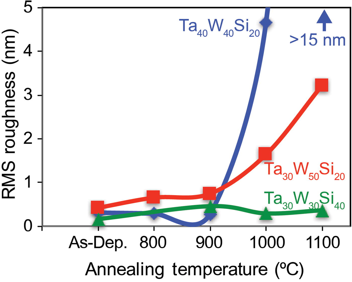
Figure 5 shows plots of surface roughness versus annealing temperature for the three TaWSi thin-film compositions. Each film is 200-nm thick and AFM surface topography images are available in the supplemental data. Below 900 °C, each film exhibits a surface roughness of a few tenths of an nm, i.e., near the noise floor of the AFM instrument. This smoothness reflects the amorphous nature of the films. Above 900 °C, the surfaces of Ta40W40Si20 and Ta30W50Si30 roughen considerably, with the roughness rising to 4.65 nm at 1000 °C for Ta40W40Si20 and 3.2 nm at 1100 °C for Ta30W50Si30. The temperature onsets for increased AFM roughness agree with phase-segregation and crystallization temperatures deduced from the x-ray data (see Fig. 3).
AFM roughness of Ta40W40Si20, Ta30W50Si20, and Ta30W30Si40 thin films after annealing between 800 and 1100 °C.

Considered design guidelines suggest stability to crystallization increases with rising refractory metal content.[Reference Zhang, Ma and Xu8] For the TaWSi system, W has the highest melting point, 3422 °C, compared with Ta, 3020 °C, and Si, 1414 °C. We find, however, that the W-rich Ta30W50Si20 thin film crystallizes approximately 100 °C lower than Ta40W40Si20 with a similar Si content. Ouyang et al.[Reference Ouyang, Wongpiya, Grubbs, Deal, Clemens and Nishi12] described a similar result, wherein a W-rich amorphous metal crystallizes at a lower temperature than that of a Ta-rich amorphous metal. These unexpected results may arise from the larger enthalpy of mixing for Ta and Si, −56 kJ/mol, compared with mixing of W and Si, −31 kJ/mol.[Reference Takeuchi and Inoue10]
An additional design rule suggests a metalloid composition of at least 20% considerably enhances amorphous-metal thermal stability.[Reference Suryanarayana and Inoue9, Reference Grubbs, Zhang, Deal, Nishi and Clemens11, Reference Ouyang, Wongpiya, Grubbs, Deal, Clemens and Nishi12] Our study confirms this guideline, as increasing the silicon content in the sputter target from 20%, Ta0W40Si20 (or Ta30W50Si20), to 40%, Ta30W30Si40, produces a composition with at least 20% Si. The high Si-content Ta30W30Si40 thin film exhibits the highest crystallization temperature. The increase in thermal stability is due to silicon's negative heat of mixing, atomic-size diversity, and strong bonds with the refractory metals as discussed in the introduction.
Oxidation behavior
Thermally robust amorphous films are envisioned to replace sputtered Ta thin films in many applications. As-deposited, 200-nm-thick Ta films generally exhibit surface roughness >1 nm, which derives from the crystalline nature of the hexagonal, β-phase. Electrical resistivities near 165 µΩ cm reflect this crystalline nature.[Reference Schauer and Roschy17] Under vacuum or inert atmosphere, the β-phase transforms to the α-phase between 700 and 800 °C. Through this transition, the electrical resistivity drops to 25 µΩ cm,[Reference Schauer and Roschy17] and the rms surface roughness rapidly exceeds 2 nm as grain-growth occurs.
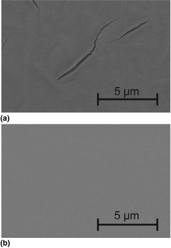
Figure 6(a) shows an SEM image of a 200-nm-thick Ta film after annealing in air at 700 °C for 10 min. Clearly, wide and deep cracks have compromised film integrity. Continued heating leads first to delamination, then conversion to Ta2O5 powder[Reference Chandrasekharan, Park, Masel and Shannon23] and complete loss of film structure. Figure 6(b) shows an SEM image of a Ta40W40Si20 thin-film surface under the same heating conditions. The film retains its smooth, featureless appearance after heating in air; oxidation negligibly affects film appearance and integrity. The rms surface roughness (0.3 nm) indicates that the film remains amorphous through the anneal. These results demonstrate the intrinsic advantages of the TaWSi formulation and its amorphous nature to produce a thermally robust, oxidation-resistant thin film that exceeds the performance characteristics of a crystalline Ta film.
(a) SEM image of the surface of a 200-nm Ta thin film after a 700 °C anneal in air for 10 min. (b) SEM image of the surface of a 200-nm Ta40W40Si20 thin film after a 700 °C anneal in air for 10 min.

Conclusions
Three new AMTFs from target compositions Ta30W50Si20, Ta40W40Si20, and Ta30W30Si40 were deposited via magnetron sputtering. XRD, electron diffraction, AFM, and TEM analyses confirmed the films to be amorphous as deposited. Electrical measurements revealed resistivities, ~200 µΩ cm, consistent with the amorphous character. Crystallization temperature increased in the order Ta30W50Si20 < Ta40W40Si20 < Ta30W30Si40. Each film exhibited stability to oxidation at temperatures above 700 °C, well above the oxidation temperature of Ta.
This study demonstrates the importance of refractory metal and metalloid contents for production of amorphous thin films that are thermally stable and resistant to oxidation at temperatures above 900 °C. Because commercial electronics already and widely employs Ta, W, and Si, tools and processes exist to integrate new and robust TaWSi films in the fabrication and manufacturing environments.[Reference Wolf and Tauber5]
Supplementary material
The supplementary material for this article can be found at https://doi.org/10.1557/mrc.2017.77
Acknowledgments
We thank the Hewlett Packard Company for financial support, Professor Brady Gibbons at Oregon State University (OSU) for the use of the AFM tool, Dr. Peter Eschbach and Teresa Sawyer in the OSU electron microscopy facility for assistance with TEM and SEM tools, and Julie Chouinard and John Donovan at the University of Oregon CAMCOR facility for assistance with EPMA measurements. This material is based upon the work supported by the National Science Foundation through the Major Research Instrumentation (MRI) Program under Grant No. 1040588. We also gratefully acknowledge financial support for the acquisition of the TEM instrument from the M. J. Murdock Charitable Trust and the Oregon Nanoscience and Microtechnologies Institute (ONAMI).