Introduction
Differential wideband band-pass filters (BPFs) possess some distinguishable advantages as compared to single ended filters. These filters have high-data rate transmission, high immunity to environmental noise better dynamic range, low-electromagnetic interference, etc. In modern wireless communication systems, a simple and compact differential wideband filter with wideband differential mode (DM) pass band and better common mode (CM) rejection capability is required. In recent years, several methods have been demonstrated in the literature for the design of wideband differential BPF [Reference Wu, Wang and Chen1–Reference Lu, Chen and Hsu9]. Second [Reference Lim and Zhu2] and sixth [Reference Lim and Zhu3] stage branch line topologies are used for the design of the wideband BPF with fractional bandwidths of 65 and 117%, respectively, but they have larger circuit size. The designs of differential ultra-wideband balanced BPFs based on a double-sided parallel-strip line were illustrated in [Reference Wang, Xue and Choi4] and [Reference Feng, Che, Eibert and Xue5]. However, in these designs, the upper stop bands for the DM were a little narrow. A compact differential BPF with a multilayer broadside-coupled structure is presented in [Reference Wu, Chu and Qiu8]. But, in this design, the presence of multiple substrate layers and metallic patterns increase the fabrication complexity. It is reported in [Reference Feng and Che10] that a T-shaped structure with the shorted/open stubs will have the differential pass band characteristics along with wide stop band features.
In this paper, the design of a compact, simple and, planar differential wideband BPF is presented. The proposed filter operates as a wideband BPF under the DM and as a wideband band stop filter under the CM. The proposed design of the filter is simulated, fabricated, and measured in order to verify the present approach. The measured pass band of the differential filter is from 5.67 to 11.01 GHz with the CM rejection better than 9.8 dB over the entire differential pass band. The measured results are in good agreement with the electromagnetic (EM) simulated results. The filter has a compact size of 0.59 λ g × 0.58 λ g, where λ g is the guided wavelength at the center frequency of the differential pass band.
This paper has four sections. After a brief overview of differential BPF and literature review, the design and analysis of the proposed filter is explained in section “design of the proposed differential wideband filter”. Results are discussed in section “results and discussion” and section “conclusion” concludes the paper.
Design of the proposed differential wideband filter
The design of the proposed differential wideband BPF is shown in Fig. 1. It comprises a circular resonator and four coupled lines. The proposed structure is a four port circuit which is symmetrical along its central plane AA′. In this design, all the parallel coupled lines are of length λ g/4 and f 0 is the center frequency of the differential pass band. The circular shaped patch resonator is chosen in the present work to make our structure symmetrical along AA″ and BB″ axes. Any regular polygon of even order (square, hexagon, octagon, etc.) may be chosen to design the differential filters. The square [Reference Serrano and Correra11], circular [Reference Tan, Chew, Leong and Ooi12], and spiral [Reference Huang13, Reference Nosrati and Mirzaee14] dual mode patch resonators have been extensively analyzed and utilized for the design of microwave filters.
Schematic of the proposed filter.

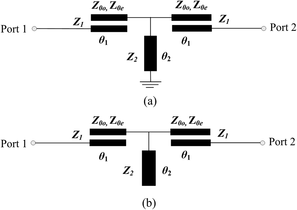
The equivalent half circuits of the proposed filter, obtained by replacing the central plane AA″ with the electric and magnetic walls, are shown in Figs 2(a) and 2(b), respectively.
Bisections of the proposed filter: (a) DM and (b) CM.

In the following subsections, these half circuits are analyzed under the DM and CM excitations.
Differential mode analysis
The equivalent circuit for DM analysis is shown in Fig. 2(a). Here, the central plane AA″ is replaced with a perfect electric wall. The semicircular resonator is replaced with its equivalent transmission line having the characteristics impedance Z 2 and electrical length θ 2. The feed lines are replaced with the parallel coupled lines (Z oo, Z oe) and the electrical length θ 1 = 90°. In the DM, the odd- and even-mode input admittances can be obtained as:
 $$\eqalign{Y_{{\rm in},\,{\rm odd}} =\; &jY_1\displaystyle{{\lpar {2\tan \theta_1-\lpar {Y_2/Y_1\tan \theta_2} \rpar } \rpar } \over {\lpar {1 + \lpar {Y_2\tan \theta_1/Y_1\tan \theta_2} \rpar -Y_1{\tan}^2\theta_1} \rpar }} \cr = &\displaystyle{{\,j\lpar {2\tan \theta_1-(Z_1/Z_2\tan \theta_2)} \rpar } \over {\lpar {Z_1 + (Z_1\tan \theta_1/Z_2\tan \theta_2)-Z_1{\tan}^2\theta_1} \rpar }}} $$
 $$\eqalign{Y_{{\rm in},\,{\rm even}} =\; &jY_1\displaystyle{{\lpar {2\tan \theta_1 + \lpar {Y_2\tan \theta_2/Y_1} \rpar } \rpar } \over {\lpar {1-{\tan}^2\theta_1-\lpar {Y_2\tan \theta_1\tan \theta_2/Y_1} \rpar } \rpar }} \cr = &\displaystyle{{\,j\lpar {2\tan \theta_1 + (Z_1\tan \theta_2/Z_2)} \rpar } \over {Z_1\lpar {1-((Z_1\tan \theta_1\tan \theta_2)/Z_2)-{\tan}^2\theta_1} \rpar }}} $$
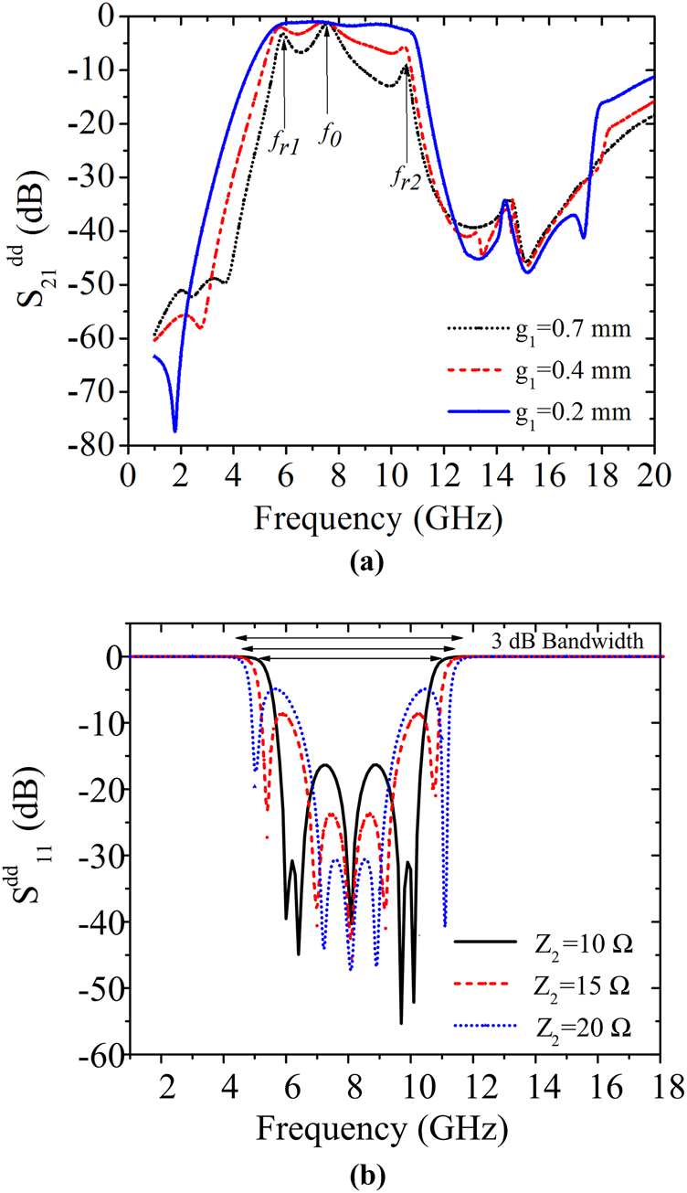
The typical frequency response of the DM obtained using transmission line circuits under weak coupling is plotted in Fig. 3(a), for different values of g 1. It can be seen that the DM has three resonant frequencies i.e. f r1 = 5.86 GHz, f 0 = 7.61 GHz, and f r2 = 10.54 GHz. The central mode corresponds to the center frequency of the differential pass band. The differential pass band can be achieved with decreasing the values of g 1.
Simulated frequency responses for DM: (a) |Sdd 21| with weak and strong couplings and (b) |Sdd 11| for different values of Z 2 (Z oe = 165 Ω, Z oo = 76 Ω, Z 1 = 120 Ω).

The circuit simulated response for various values of Z 2 are plotted in Fig. 3(b). Keysight Technologies Advance Design System (ADS) is used to carry out these simulations. It may be observed that the more bandwidth of the DM circuit can be achieved with an increase in the value of Z 2. However, it results in the degradation of the return loss. Therefore, the optimum value for Z 2 is taken as 15 Ω. The 3-dB bandwidth for Z 2 = 15 Ω is 5.65 GHz (5.36–11.01 GHz).
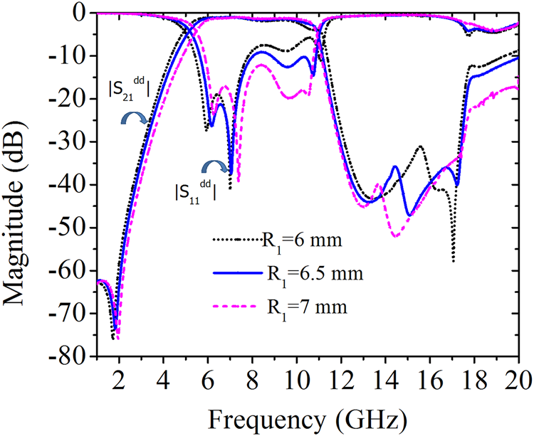
The numerically simulated frequency response of the proposed filter for different values of R 1 is shown in Fig. 4. It may be observed that the return loss characteristics of the differential filter become better with increasing values of R 1. However, increasing R 1 leads to the reduction in the pass band bandwidth.
EM simulated frequency responses for different values of R 1.

Common mode analysis
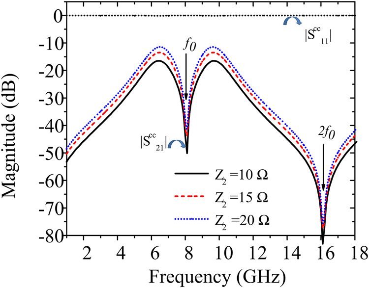
For the CM operation, the central plane AA″ is replaced a perfect magnetic wall and the corresponding CM equivalent circuit is shown in Fig. 2(b). The circuit simulated S-parameters for the different values of Z 2 are shown in Fig. 5. It is observed that an increase in the value of Z 2 improves CM rejection. However, the DM return loss gets worsen with increasing Z 2 as we have seen in Fig. 3(b). Hence, Z 2 = 15 Ω provide the good return loss in DM and good rejection (better than 10 dB) for the CM operation.
Simulated frequency responses of the CM with |Scc 21| and |Scc 11| (Z oe = 166.6 Ω, Z oo = 85.6 Ω, Z 1 = 124 Ω).

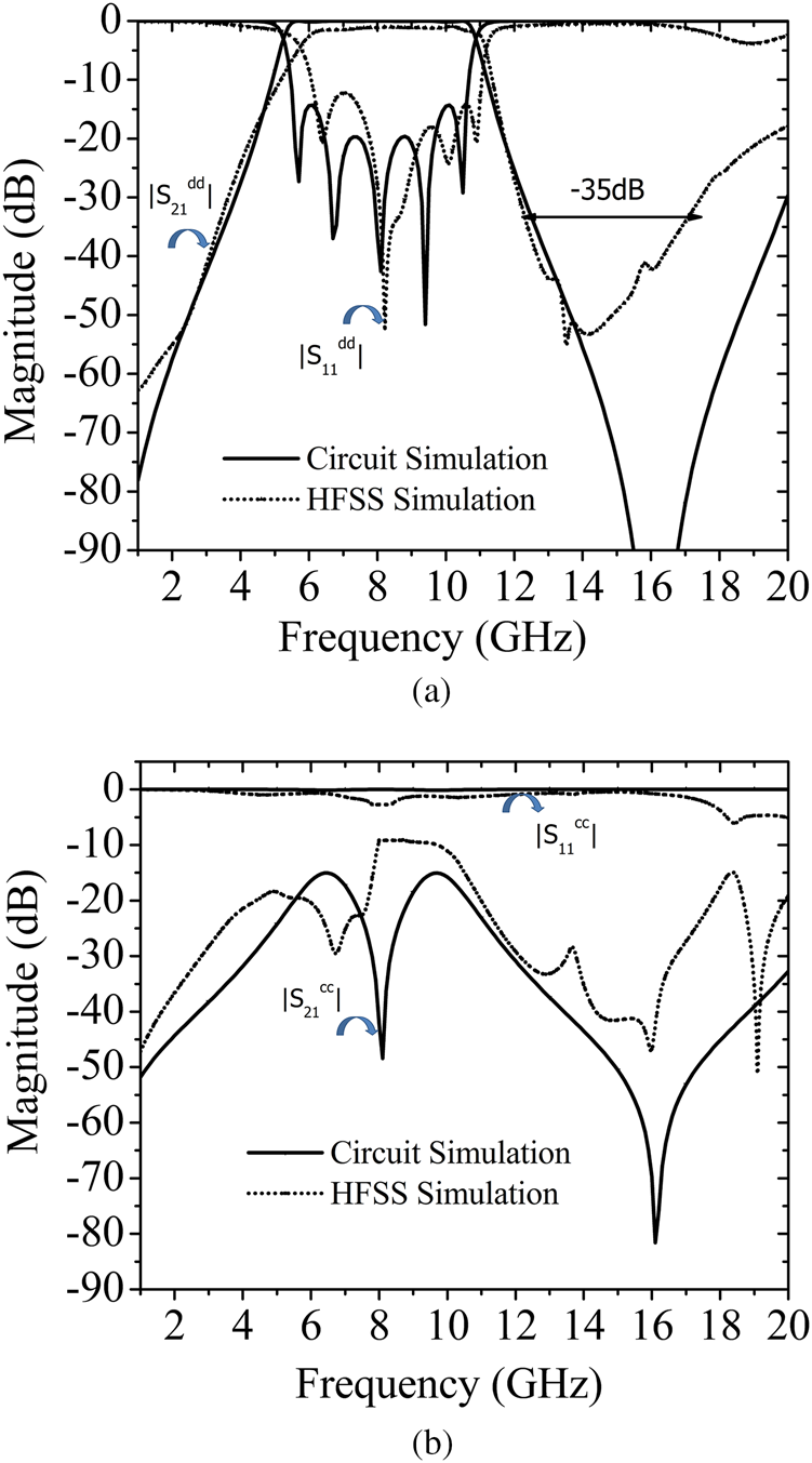
Based on the above analyses, the circuit simulations of the proposed differential wideband band are performed and compared with its EM simulated results and are plotted in Fig. 6. Figure 6(a) shows the simulated response under the DM operation and Fig. 6(b) for the CM operation. The circuit simulated responses matches well the EM simulated responses. However, there is little mismatch in the CM response.
Simulated results for the proposed differential BPF: (a) DM and (b) CM.

Results and discussion
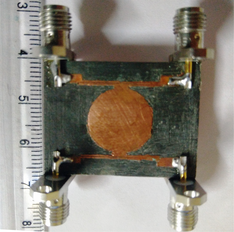
The proposed differential wideband BPF is fabricated on the RT/duroid 5880 substrate. The substrate is having a dielectric constant of 2.2, a loss tangent of 0.0009, and a thickness of 0.787 mm. Figure 7 shows the photograph of the fabricated prototype filter. The optimized design parameters for the proposed differential BPF are obtained as (here, all dimensions are in mm): W 0 = 2.425, l 1 = 7.5, l 2 = 15.8, g 1 = 0.2, g 2 = 0.2, R 1 = 6.5, D = 14, w 1 = 0.2, S = 2.54, tl 1 = 0.8, and tw 2 = 2.4.
The fabricated wideband differential BPF.

The S-parameters of the fabricated filter is measured using Keysight 5071 C vector network analyzer. The proposed filter has a compact size of 15.8 mm × 15.6 mm, which corresponds to 0.59 λ g × 0.58 λ g, where λ g is the guided wavelength at the center frequency of the differential pass band. The differential and CM S-parameters of the proposed differential BPF can be extracted by using four port S-parameters as [Reference Eisenstant, Stengel and Thompson15]:
 $$S_{21}^{dd} = \lpar {S_{21}-S_{2^{\prime}1}-S_{21^{\prime}} + S_{2^{\prime}1^{\prime}}} \rpar /2$$
 $$S_{11}^{dd} = \lpar {S_{11}-S_{1^{\prime}1}-S_{11^{\prime}} + S_{1^{\prime}1^{\prime}}} \rpar /2$$
 $$S_{21}^{cc} = \lpar {S_{21} + S_{2^{\prime}1} + S_{21^{\prime}} + S_{2^{\prime}1^{\prime}}} \rpar /2$$
 $$S_{11}^{cc} = \lpar {S_{11} + S_{1^{\prime}1^{\prime}} + S_{11^{\prime}} + S_{1^{\prime}1^{\prime}}} \rpar /2$$
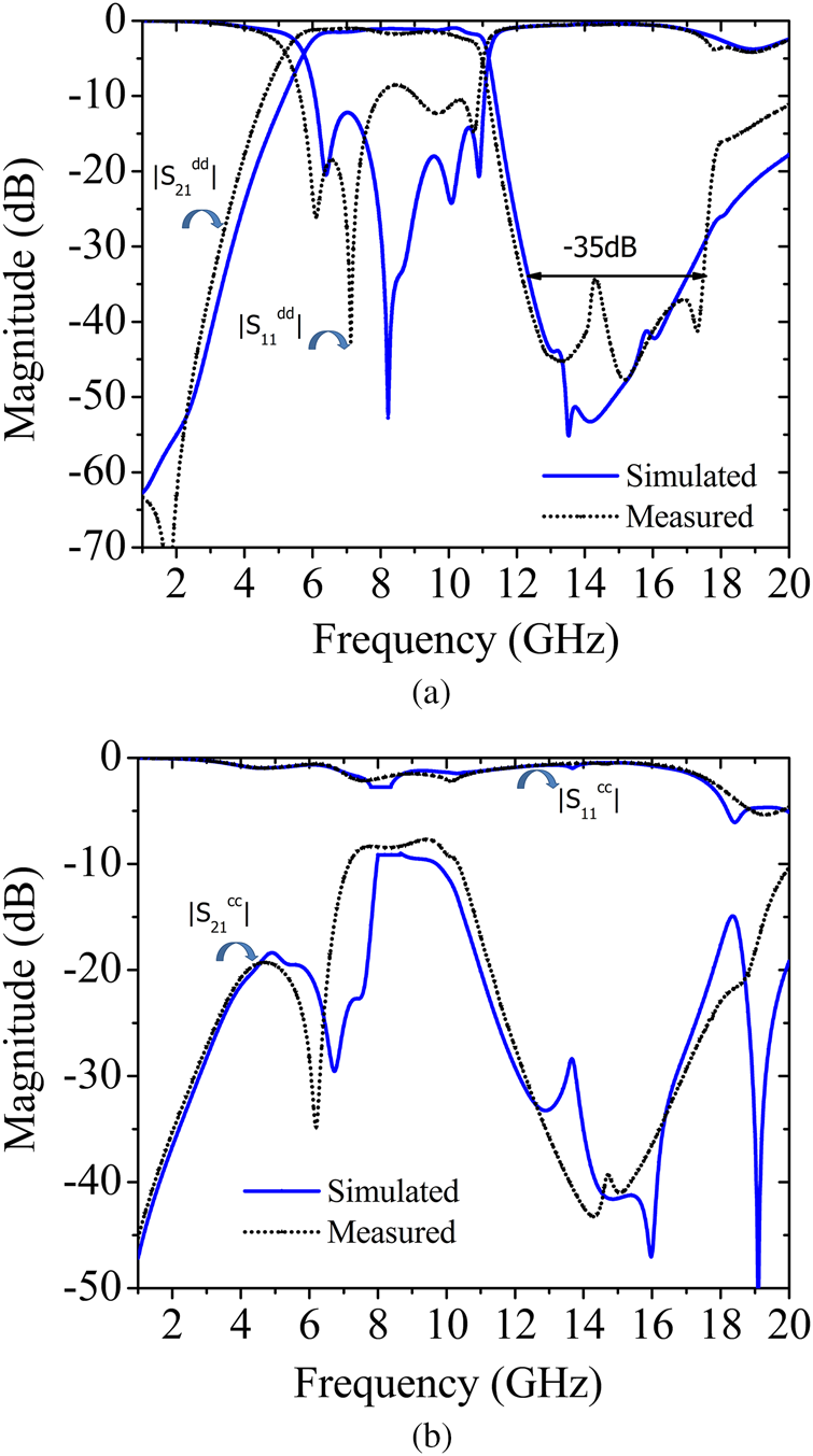
The simulated and measured S-parameters of the proposed filter are shown in Fig. 8. The proposed filter has the wideband differential pass band, which lies from 5.67 to 11.18 GHz. The CM rejection bandwidth of the filter is from 1 to 20 GHz with the rejection better than 10 dB over the entire differential pass band.
Simulated and measured results for the differential filter of Fig. 1: (a) DM and (b) CM.

The measured differential pass band bandwidth is 5.65 GHz (5.36−11.01 GHz), and the 3 dB fractional bandwidth is 70% with the minimum insertion loss of 1.6 dB over the pass band. The measured CM rejection level is better than 9.8 dB over the measured differential pass band bandwidth. The proposed filter is having attenuation better than 35 dB in the upper stop band (12.5−18 GHz), which indicates its good out-of-band performance.
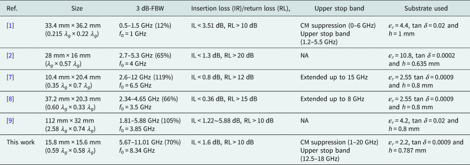
A comparison of the proposed differential filter with the other similar works reported in the literature is presented in Table 1. Our proposed differential filter has comparable performance with the others.
Comparison of the proposed differential filter with the other reported in the literature

Conclusion
The design of a circular-shaped differential wideband filter is presented. The analysis of the proposed structure shows that it possesses the characteristics of the wideband BPF under the DM. In addition, the proposed filter has wideband band stop characteristics under the CM. The compact size along with the wide differential pass band and good CM rejection makes the proposed structure suitable for the next generation portable balanced communication systems.
 Dharmendra Kumar Jhariya was born on 1987, in India. He received his Bachelor's Degree (B.E.) in Electronics & Communication Engineering from R.G.P.V. Bhopal (M.P.) in 2009 and completed the M.Tech.in ECE (Digital Systems) from M.N.N.I.T., Allahabad (U.P) in 2011 and received his PhD degree from I.I.T. Kharagpur, India. His current research interests include in filter design. His research papers publication in MOTL and IJMWT (Cambridge University Press). He has joined Jaypee Institute of Information Technology, Noida Sector-62, in July 2017 as an Assistant Professor (Senior Grade).
 Dr. Akhilesh Mohan received B. Tech. degree in Electronics Engineering from the K.N.I.T. Sultanpur, India, in 2002, M.Tech, and Ph.D. degree in microwave engineering from the I.I.T. Kanpur in 2004 and 2009 respectively. He worked as a Scientist/Engineer at Space Applications Center, Indian Space Research Organization, Ahmadabad from Feb. 2008 to July 2010. Since May, 2013, he is working as an Assistant Professor in E&ECE Department at I.I.T. Kharagpur, India. He has authored or co-authored over 50 peer reviewed international journal and conference papers.
 Dr. Rahul Kaushik received his B. Tech. (Electronics and Telecommunication Engineering) and M.Tech. from University of Allahabad, India in 2001 and 2003 respectively. He received his Ph. D. Degree from Jaypee Institute of Information Technology (JIIT), Noida, India in 2017. Presently, he is working as Assistant Professor (Senior Grade) in the department of ECE at JIIT, Noida, India. His research interests lie in the areas of communication systems. He is a senior member of the IEEE, USA and a fellow of IETE, India.
 Vishal Narain Saxena was born in 1988 in India. He received his B.Tech degree from Galgotias College of Engineering and Technology (GCET), Greater Noida in 2009 and M.Tech degree from IIT Roorkee in 2011 and is now pursuing Ph.D. from JIIT Noida, India. His current research interests include radio frequency and microwave engineering, and wireless communication. Currently he is an assistant professor in the Department of Electronics and Communication Engineering, Jaypee Institute of Information Technology, Sector 62, Noida, India.