I. INTRODUCTION
The active region of a wafer-based semiconductor device typically occupies only a small fraction of the wafer thickness, resulting in unnecessarily high materials costs for a wide range of devices such as solar cells, LEDs, lasers, and transistors. Single crystal thin films attached to inexpensive support substrates can replace wafers, and be used to make equivalent, if not better, devices, but with lower materials costs and the possibility of mechanical flexibility. In principle, there are two ways to accomplish this. One can either separate a thin layer from a single crystal wafer or ingot, or, one can use a single crystal as a substrate for epitaxial growth of a single crystal thin film, which is then removed from the substrate. In both cases, the goal is to reuse the wafer or ingot as many times as possible to keep material costs to a minimum. Based on these principles, several approaches have been explored over the last 30 years or so, including (i) epitaxial Si separation via porous Si perforation layers,Reference Brendel1 (ii) layer spalling via stressed overlayers,Reference Rao, Mathew, Saha, Smith, Sarkar, Garcia, Stout, Gurmu, Onyegam and Ahn2–Reference Martini, Gonzalez, Dross, Masolin, Vaes, Frederickx and Poortmans4 (iii) layer separation via ion-implantation-induced microcracks,Reference Bruel5 (iv) and liftoff of epitaxial GaAs via lateral chemical (HF) etching of GaxAl1−xAs release layers.Reference Yablonovitch, Gmitter, Harbison and Bhat6
Although these efforts represent substantial progress toward these goals, each technique suffers from at least one major limitation. In the first three techniques, separation of the thin film from its single crystal substrate relies on some form of cleavage, which is efficient from a throughput and materials utilization standpoint; however, the location of fracture is not precisely controlled, resulting in films with high surface roughness (techniques i, iii), thickness variation (ii, iii), and poor thickness accuracy (ii, iii). In process iv, however, the film's separation plane is controlled by the location of the thin GaxAl1−xAs buffer layer, resulting in films with well-defined uniform thicknesses and smooth surfaces. Unfortunately, this process is hindered by slow (∼3 cm/h) lateral etch rates,Reference Schermer, Mulder, Bauhuis, Voncken, van Deelen, Haverkamp and Larsen7 and by challenges in lifting-off completed devices due to hydrofluoric acid's (HF) damaging effect on metal and oxide layers during the long immersion in HF.
We present a new approach for obtaining single crystal thin films attached to inexpensive support substrates. In our approach, we grow an epitaxial thin film on a single crystal growth template. Then, the epitaxial thin film is adhered to a support substrate and is separated from its growth surface via fracture along the heteroepitaxial interface between the film and its growth substrate or, alternatively, via fracture along a heteroepitaxial interface of an epitaxial buffer layer between the film and the growth substrate. By fabricating an epitaxial structure with a mechanically weak heteroepitaxial interface, or a structure with a heteroepitaxial interface that can be weakened by a chemical species to exhibit environmentally assisted cracking, we precisely control the location of fracture, resulting in a process with the controllability of the GaxAl1−xAs etching technique (process iv) and the speed and etchant-free qualities of cracking techniques (processes i–iii).
In our example system, we show that films of epitaxial Si, Ge, and GaAs with thicknesses ranging from 100 nm to 1 μm grown on epitaxial CaF2 overlayers on Si <111> substrates can be transferred to glass substrates by inducing fracture along the heteroepitaxial interface between the semiconductor thin film and CaF2, or between CaF2 and the Si wafer. Furthermore, we show that water increases the ease of fracture along these interfaces, presumably by weakening the heteroepitaxial interfaces between the semiconductor thin film and CaF2 and/or between CaF2 and the Si wafer as in moisture-assisted cracking. We also study this effect by observing the spontaneous delamination of stressed Si and Ge films grown on CaF2 <111> single crystals when exposed to water-containing gases. Last, using x-ray diffraction, we examine the structural quality of our epitaxial films, and we show that no morphological changes occur to these films as a result of our liftoff procedure by comparing x-ray data taken on these films from before and after liftoff.
II. EXPERIMENTAL
A. Liftoff experiments
Si <111> substrates coated with a thin (100 nm–1 μm) epitaxial CaF2 layer were used as growth substrates for the growth of epitaxial Si, Ge, and GaAs films with thicknesses ranging from 100 nm to 1 μm. Prior to CaF2 deposition, the Si <111> substrates were etched with dilute HF to remove the native SiO2 layer. Using e-beam evaporation, CaF2 films were deposited at a deposition rate of 0.6 Å/s with a substrate temperature of 720 °C, and Si and Ge films were deposited on the CaF2-coated Si <111> substrates at a deposition rate of 1 Å/s with substrate temperatures of 600 °C, and 720 °C, respectively. For all e-beam evaporations, the background pressure was approximately 3 × 10⁻⁸ Torr. Deposition of GaAs onto CaF2-coated Si <111> substrates was performed using an Aixtron AIX 200/4 MOCVD reactor (Herzogenrath, North Rhine-Westphalia, Germany) with a substrate temperature of 700 °C, an Ar pressure of 75 Torr, tertiarybutylarsine (TBAs) flow of 242 μmol/min, trimethylgallium (TMGa) flow of 17.5 μmol/min, and disilane flow of 16.7 nmol/min.
For the Si and Ge films, a 5-nm-thick carbon film was deposited along the perimeter of the CaF2 surface to serve as a crack initiation region between the CaF2 surface and the subsequently deposited Si or Ge thin film. The carbon layers were deposited using e-beam evaporation with a deposition rate of 0.5 Å/s and a substrate temperature of 20 °C. For the GaAs films, this carbon layer was not used because it was observed that GaAs does not form a continuous film on carbon, thereby preventing the carbon from serving as a crack initiation layer for the GaAs film.
After deposition of the Si, Ge, or GaAs film, a 3-mm-thick glass substrate coated with uncured epoxy was placed on the surface of the epitaxial semiconductor film. For the Si and Ge films, the glass substrate was placed such that one edge of the glass rested within the region directly above the carbon layer. The structure was then placed on a hotplate maintained at 200 °C for 3 min to cure the epoxy. The epoxy used was EpoxyBond 110 from Allied High Tech Products Inc. (Rancho Dominguez, CA). This epoxy remains liquid until rapid curing occurs when the epoxy reaches approximately 150 °C, thus solidifying while the structure is hot, thereby generating stress upon cooling due to differences in thermal expansion coefficients between the growth substrate, the epoxy, and the glass substrate.
Once cooled to room temperature, the tip of a razor blade was placed at the edge of the glass substrate (the edge above the carbon layer for the Si and Ge samples) where it was glued to the film structure at approximately 80° from substrate normal. Then, a moderate force (0.25–5 lbs) was manually applied to the razor blade so as to wedge the blade between the glass and Si substrates, causing the glass substrate to break free from the Si substrate, with the semiconductor film remaining adhered to the glass substrate.
B. Growth on CaF2 <111> single crystal substrates
Si and Ge films were deposited on CaF2 <111> single crystal substrates using electron beam evaporation at a deposition rate of 1 Å/s with a substrate temperature of 600 °C and a background pressure of approximately 3 × 10⁻⁸ Torr. The epitaxial quality of the Si and Ge films was monitored in situ with reflected high-energy electron diffraction during growth. Upon reaching room temperature after deposition, the samples were transferred to a load lock where the samples were then exposed to dry N2, O2, Ar, air, and N2 bubbled through deionized water. Spontaneous delamination of these epitaxial films was observed through a glass viewing port installed on the load lock.
C. X-ray diffraction experiments
To determine the epitaxial quality of the Si, Ge, and GaAs films grown on the CaF2-coated Si <111> substrates and to detect morphological changes to these films as a result of the liftoff process, x-ray diffraction was performed before and after the liftoff process, using symmetric θ–2θ scans, rocking curves of the (111) film peaks, and ϕ scans of the (220) film peaks. In the rocking curves, the x-ray diffractometer was aligned to the (111) diffraction peak and then the sample was rocked through an angle ω about an axis lying in the plane of the sample. The shape of this peak reflects in-plane coherence length as well as the degree of crystallographic alignment in the out-of-plane direction. In the ϕ scans, the x-ray diffractometer was aligned to the (220) diffraction peak of the film. At this position, the scattering vector is tilted approximately 35.3° from substrate normal, and thus has a component in the plane of the sample. The sample was then rotated about its surface normal through the angle ϕ. The shape of the resulting peak reflects the in-plane coherence length as well as the degree of crystallographic alignment in the in-plane direction.
III. RESULTS AND DISCUSSION
A. Liftoff experiments
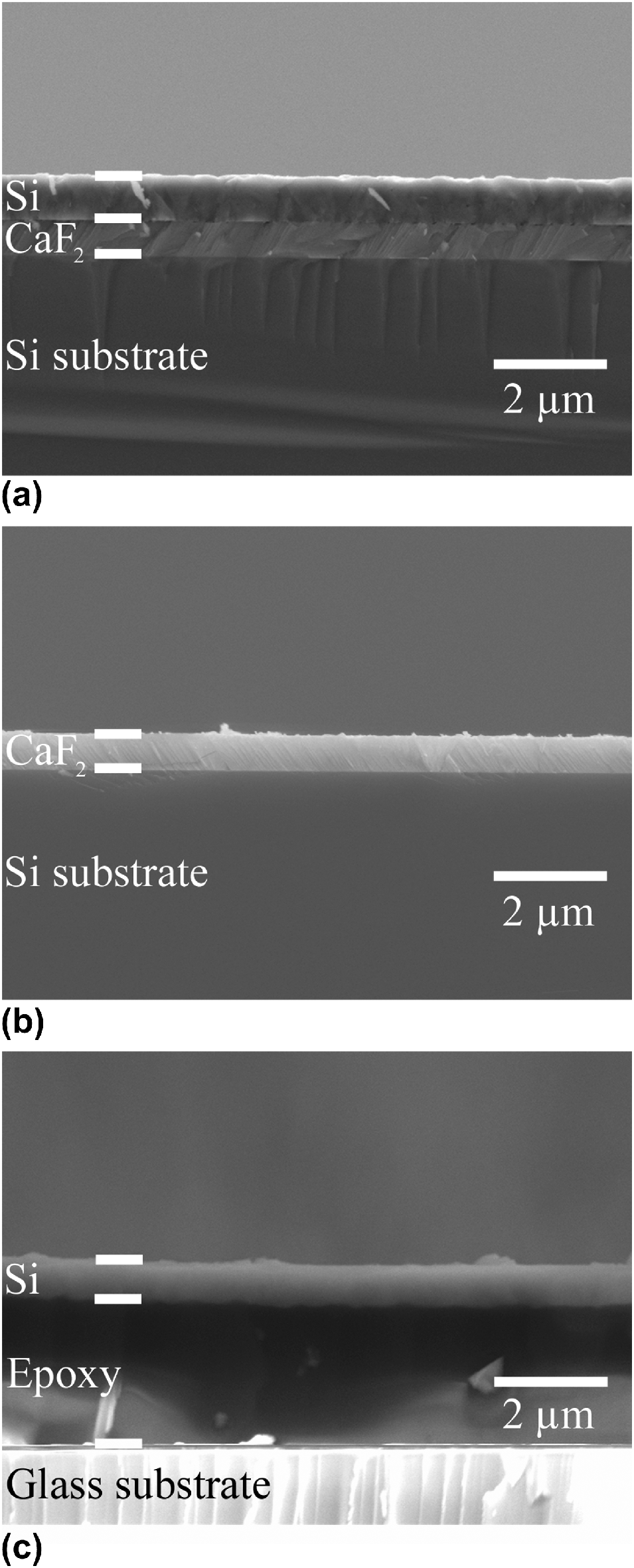
Upon application of force with a razor blade, the glass substrates break free from the Si substrate, leaving the semiconductor film adhered to the glass substrate with epoxy (Figs. 1 and 2). For some samples, fracture occurred almost exclusively along the upper heteroepitaxial interface between CaF2 and the semiconductor thin film (right sample in Fig. 1), whereas for other samples (left and middle samples in Fig. 1), the fracture surface alternated between the upper heteroepitaxial interface and the lower heteroepitaxial interface (CaF2/Si wafer interface), resulting in regions of CaF2 adhered to both the thin film and the Si wafer after liftoff (Fig. 3). However, with a short (20 s) immersion in sulfuric acid, these residual CaF2 regions can be easily removed from both the semiconductor film and the growth substrate, thereby restoring the Si wafer for reuse and exposing the smooth surface of the semiconductor thin film (Fig. 3). For samples where fracture occurred exclusively along the upper heteroepitaxial interface, we have shown that the CaF2 layer can be reused for growth of additional epitaxial semiconductor thin films.
Epitaxial Si films of 500-nm thickness adhered to glass support substrates and the growth substrate from which they were separated. The films were grown on a 250-nm-thick epitaxial CaF2 buffer layer on a Si <111> substrate. In the rightmost sample, fracture occurred almost exclusively along the heteroepitaxial interface between the Si film and the CaF2 layer. For the left and middle samples, fracture occurred along both heteroepitaxial interfaces, resulting in patches of CaF2 adhered to both surfaces after liftoff. The fracture surface of the left sample is shown in Fig. 3. The left and middle Si films are adhered to soda-lime glass substrates, whereas the film on the right is adhered to a borosilicate glass substrate. The dark line along the straight edge of the Si <111> substrate is from the 5-nm-thick carbon layer.

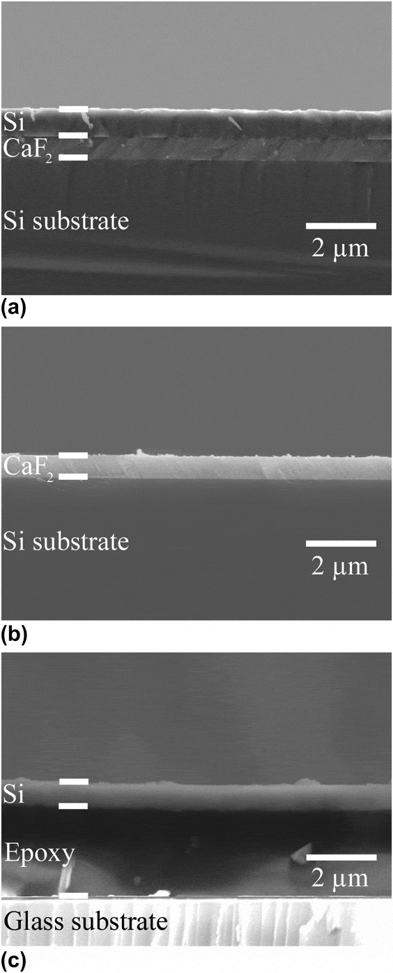
SEM cross-section of a typical epitaxial Si film adhered to a borosilicate glass substrate before and after liftoff. (a) Shows an epitaxial Si film grown on an epitaxial CaF2 layer on top of a Si <111> substrate before liftoff; (b) shows the CaF2 overlayer on the Si <111> substrate after liftoff of the Si film; and (c) shows the Si film adhered to the glass substrate after liftoff.
Typical fracture surface after liftoff of a Si film adhered to a soda-lime glass substrate. (a) Shows an optical micrograph of the fracture surface of the left sample shown in Fig. 1. The majority phase with the yellow/green color is CaF2. (b) Shows an optical micrograph of the same fracture surface after the removal of CaF2 via a short (20 s) immersion in sulfuric acid.
We observed that the composition of the glass support substrate helps to determine whether the crack will alternate between the two heteroepitaxial interfaces or remain at the upper heteroepitaxial interface. Soda-lime glass substrates, with thermal expansion coefficients of α ≈ 8 × 10⁻⁶ K−1, typically result in fracture surfaces alternating between the two heteroepitaxial interfaces, whereas borosilicate glass substrates, with α ≈ 3.3 × 10⁻⁶ K−1, typically result in fracture almost exclusively at the upper heteroepitaxial interface. Since the borosilicate glass has a thermal expansion coefficient closer to that of the Si substrate (α ≈ 2.6 × 10⁻⁶ K−1), cooling from the epoxy cure temperature creates less stress than the case of soda-lime glass, resulting in less of a tendency for the crack to dive to the lower interface.
During liftoff of Si films grown on epitaxial CaF2 overlayers on Si <111> substrates, we observed a decrease in fracture toughness of both heteroepitaxial interfaces with increased exposure to water. For these Si films, cooling from the epoxy cure temperature results in spontaneous partial delamination. Typically, spontaneous delamination starts from the carbon-coated crack initiation region, then propagates along the two edges perpendicular to the crack initiation region before ceasing further delamination, resulting in a horseshoe-shaped delaminated region. We observed that the final size of this delaminated region is influenced by the amount of water to which the sample is exposed. For example, for a 1-cm2 Si film adhered to a soda-lime glass substrate cured in an N2 glove box, approximately 15% of the sample area delaminated upon cooling in the glovebox. Next, the same sample was removed from the glovebox and exposed to air (∼50% humidity), resulting in the delamination of an additional ∼10% of the sample area. Then, the same sample was immersed in deionized (DI) water, resulting in the immediate delamination of an additional ∼15%.
A fracture will cease to propagate when the stress intensity factor, which is solely a function of the sample geometry and stress state, falls below the critical stress intensity needed for crack propagation.Reference Anderson8 For our Si films, the transfer of the sample from the glovebox to air should not change the stress intensity factor, since neither the sample geometry nor the stress state changes during transfer. The observation of continued delamination upon exposure to air therefore demonstrates a reduction of the critical stress intensity factor. The same argument holds for the transfer of the sample from air to the liquid water environment. The reduction of the critical stress intensity factor of the sample due to water means that water effectively weakened the interfaces along which the crack propagated, i.e., the heteroepitaxial interfaces between the Si film and CaF2, and/or between CaF2 and the Si substrate, through moisture-assisted cracking.
B. Growth on CaF2 <111> single crystal substrates
To further explore the effect of water on cracking at these heteroepitaxial interfaces, epitaxial thin films of Ge and Si were grown on single crystal CaF2 <111> substrates using electron beam evaporation. Both films were grown at 600 °C, and due to the large differences in thermal expansion between the CaF2 <111> substrate with α ≈ 25 × 10−6 K−1,Reference Schumann and Neumann9 and these semiconductor films with α's between 2.6 × 10⁻⁶ K−1 and 5.9 × 10⁻⁶ K−1,Reference Slack and Bartram10 the films were in compression upon reaching room temperature. Upon reaching room temperature after deposition, the films were stable in vacuum, dry N2, O2, and Ar. However, immediately upon exposure to air, or N2 bubbled through deionized water, the films rapidly and spontaneously delaminated from their CaF2 growth substrates. For both samples, delamination originated at the samples' edges and worked inward at speeds of approximately 1 mm/s along the heteroepitaxial interface, resulting in highly buckled films resting atop their CaF2 growth substrates after delamination (Fig. 4). This spontaneous delamination observed for films grown on single-crystal CaF2 substrates was not observed for films grown using the same growth conditions on CaF2 buffer layers on Si substrates. Presumably this is due to the difference in thermal expansion mismatch.
Delaminated Ge film grown on a CaF2 <111> substrate at 600 °C using electron beam evaporation. The film was stable in vacuum, dry N2, O2, and Ar, however delaminated immediately when exposed to air, with a delamination front speed of approximately 1 mm/s. Upon release, the film expanded laterally but remained lightly adhered at the edges of the substrate, giving rise to the buckled appearance. Immersing the debonded film and the substrate in water and gently agitating the water, the film released from the substrate completely.
The buckled nature of the delaminated film in Fig. 4 shows that the film underwent a lateral expansion upon delamination, and therefore was in compression prior to delamination as is expected, given CaF2's larger thermal expansion coefficient. Because the stressed film was stable in the absence of water and delaminated immediately upon exposure to water vapor, we conclude that the water vapor weakened the heteroepitaxial interface, providing conclusive evidence to the existence of environmentally assisted cracking along these heteroepitaxial interfaces and further evidence that water is the active chemical species.
The mechanism of moisture-assisted cracking along heteroepitaxial interfaces of CaF2 with Si, and with Ge, is unclear at this point. One possibility is that water acts as a catalyst for the breaking of bonds between the semiconductor materials and Ca and/or F. Another possibility is that there is a stress-enhanced chemical reaction between water and the semiconductor, and/or between water and CaF2, thereby breaking the CaF2/semiconductor bonds and causing delamination.
C. X-ray diffraction measurements
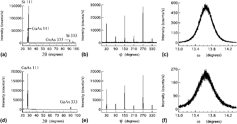
The liftoff procedure we have described does not induce morphological changes to the films, as evidenced by x-ray diffraction data taken before and after liftoff (GaAs XRD data shown in Fig. 5). The before and after full width half max (FWHM) values for the GaAs (220) peaks in ϕ [shown in Figs. 5(b) and 5(e)] were both 0.7°. The before and after FWHM values for the GaAs (111) rocking curves in ω [shown in Figs. 5(c) and 5(f)] were 0.36 and 0.42°, respectively. The FWHM values for Ge (111) rocking curves taken before and after liftoff were 0.28 and 0.29°, respectively, and the FWHM of the Ge (220) ϕ scans taken before and after liftoff were both 0.48°. For both GaAs and Ge, we measured no change in the FWHM of the (220) ϕ scans, however, for both films, the rocking curve width increased slightly after the liftoff process. We believe this is possibly due to slight bending of the film adhered to the glass substrate, especially at the sample's edges. It was not possible to obtain rocking curve data or ϕ scan data from the Si films before liftoff due to interference with the Si substrate peaks; however, the post liftoff FWHM of the Si (111) rocking curve was 0.79° in ω and the post liftoff FWHM of the Si (220) peaks in ϕ was 1.27°.
X-ray diffraction data for a GaAs film grown on an epitaxial CaF2 layer on top of a Si <111> substrate. Shown are results in the as-grown state, and after bonding to a glass carrier and delamination from the Si <111> substrate. (a) and (d) show symmetric θ–2θ scans for as-grown and delaminated films [note the presence of the Si <111> substrate peaks in (a), absent in (d)]; (b) and (e) show GaAs (220) ϕ scans for as-grown and delaminated films, and (c) and (f) show GaAs (111) rocking curves for as-grown and delaminated films.
In the (220) ϕ scans of all three materials, two sets of peaks were observed, with one low-intensity set offset by 60° from the higher intensity peaks, as shown in Figs. 5(b) and 5(e) for the GaAs film. This is due to a mixture of type A and B epitaxial orientations at the heteroepitaxial interface between the semiconductor film and CaF2, and/or between CaF2 and the Si substrate.Reference Olmstead and Bringans11
The large widths in ω and ϕ measured in all three materials indicate that all three films contain structural defects. Based on the XRD data, the Ge films were of highest crystalline quality, followed by GaAs, followed by Si. From lattice mismatch alone, we would expect Si to have the lowest widths in ω and ϕ since Si is more closely matched to CaF2; however, we observe less width in ω and ϕ with Ge and GaAs than with Si. We attribute this to higher homologous temperatures for Ge and GaAs during film growth. That is, 600 °C and 700 °C (growth temperature for Ge and GaAs, respectively) represent larger fractions of the melting temperatures of Ge and GaAs (937 °C and 1238 °C, respectively) than 720 °C (growth temperature for Si) is to the melting temperature of Si (1410 °C). It is likely that a higher homologous temperature enables higher adatom mobility, allowing adatoms to more easily arrange themselves into a configuration with lower free energy, thus higher crystalline perfection.
We have not yet optimized our epitaxial growth parameters; however, other groups have done so, and have made significant progress toward growing high quality epitaxial films of Ge, Si, and GaAs on CaF2 and related fluoride material surfaces.Reference Schroeder, Meng, Bostwick, Olmstead and Rotenberg12–Reference Sinharoy15 We predict that the use of more optimized growth procedures should not alter the liftoff procedure nor the moisture-assisted cracking mechanism we have observed in this system.
IV. CONCLUSION
A new approach for creating single crystal thin films attached to inexpensive support substrates is introduced. In this approach, epitaxial thin films are separated from their growth substrates by means of cracking along a mechanically weak heteroepitaxial interface. We have demonstrated this approach by showing that films of epitaxial Si, Ge, and GaAs with thicknesses ranging from 100 nm to 1 μm can be rapidly cracked from their CaF2 growth surfaces and transferred to a glass substrate, and we have shown with XRD that no morphological changes occur to these films as a result of the liftoff process. The approach we have outlined is believed to be general, and applicable to other epitaxial material systems with heteroepitaxial interfaces that are weak and/or susceptible to chemical weakening. The application of this approach to new epitaxial systems could result in new form factors for a wide range of electronic devices as well as dramatic cost savings since the growth substrate material is not consumed in this process and therefore can likely be reused many times with minimal processing between iterations.
ACKNOWLEDGMENTS
The authors would like to thank NSF for supporting Garrett Hayes with a graduate research fellowship; Chinmay Nivargi, Alberto Salleo, and Nicholas Melosh for helpful discussions; and Vijay Parameshwaran for assistance in depositing MOCVD GaAs films.
This material is based upon work supported by the Department of Energy through the Bay Area Photovoltaic Consortium under Award Number DE-EE0004946. Disclaimer: This report was prepared as an account of work sponsored by an agency of the United States Government. Neither the United States Government nor any agency thereof, nor any of their employees, makes any warranty, express or implied, or assumes any legal liability or responsibility for the accuracy, completeness, or usefulness of any information, apparatus, product, or process disclosed, or represents that its use would not infringe privately owned rights. Reference herein to any specific commercial product, process, or service by trade name, trademark, manufacturer, or otherwise does not necessarily constitute or imply its endorsement, recommendation, or favoring by the United States Government or any agency thereof. The views and opinions of authors expressed herein do not necessarily state or reflect those of the United States Government or any agency hereof.