I. INTRODUCTION
The promise of achieving specific functional properties through nanostructure motivates substantial synthetic efforts to prepare new and unconventional materials. Developing an understanding of the exceptional properties of such materials is of key importance. Toward these aims, we have recently developedReference Heideman, Nyugen, Hanni, Lin, Duncombe, Johnson and Zschack1–Reference Lin, Smeller, Heideman, Zschack, Koyano, Anderson, Kykyneshi, Keszler, Anderson and Johnson3 a general synthetic approach to the preparation of new families of thin film intergrowth compounds, derived from layered linear intergrowthsReference Wiegers4 of rock salt-like monochalcogenide (e.g., PbSe, BiSe, etc.) and transition metal dichalcogenide components (e.g., WSe2, NbSe2, etc.), using the method of modulated elemental reactants (MER).Reference Noh, Johnson, Hornbostel, Thiel and Johnson5 These novel nanolaminate materials exhibit exceptionally low thermal conductivities, on the order of 0.1 W·m−1·K−1 and 0.4–0.5 W·m−1·K−1, perpendicular and parallel to the layering, respectively.Reference Chiritescu, Cahill, Heideman, Lin, Mortensen, Nguyen, Johnson, Rostek and Böttner6, Reference Mavrokefalos, Lin, Beekman, Seol, Lee, Kong, Pettes, Johnson and Shi7 These extremely low thermal conductivities can be attributed to the unusual nanostructure that can be described as “turbostratic” disorder,Reference Chiritescu, Cahill, Nguyen, Johnson, Bodapati, Keblinski and Zschack8 a key aspect which also makes them structurally distinct from the bulk misfit-layered compounds from which the nanostructure of these materials is derived.Reference Wiegers4
The controllable “nano-architecture” in material systems such as these new misfit-layered compounds presents a potential route to tunable physical properties, in particular with respect to electrical transport and thermoelectric properties. However, a key challenge that must be overcome is control of the distribution of compositional and structural defects inherently trapped by the low temperature, nonequilibrium nature of the synthetic route.Reference Lin, Heideman, Nguyen, Zschack, Chiritescu, Cahill and Johnson2, Reference Smalley, Kim and Johnson9 Consequently, it is of interest to identify potential methods for reducing defect levels in these thin film specimens in order that the physical properties of these and related materials, as well as the influence of nanostructure, order, and disorder, can be accurately assessed.
Annealing in a controlled atmosphere of the most volatile elemental constituent has been shown previously to be effective in fixing the carrier concentration in thermodynamically stable compound semiconductor crystals, such as GaP (phosphorous vapor),Reference Nishizawa, Okuno, Suto, Sato and Yamokoshi10 Bi2Te3 (tellurium vapor),Reference Fleurial, Gailliard, Triboulet, Scherrer and Scherrer11 and PbxSn1−xTe-based compounds.Reference Sugiyama12 These approaches utilize thermodynamic equilibria between the crystalline and vapor phases, allowing control of electrically active compositional and structural defects which influence electrical transport properties. The application of such postprocessing approaches to kinetically stable materials, however, remains relatively unexplored. This motivated us to initiate systematic studies of the influence of specimen annealing, under controlled partial pressures of selenium vapor, on the electrical transport properties of the recently discovered misfit-layered nanolaminates. Here, we report the effects on room temperature carrier concentration, Seebeck coefficient, and Hall mobility for [(PbSe)0.99]1[WSe2]1 specimens. Composed of one layer of PbSe and one layer of WSe2, this new misfit-layered compound may be categorized as a moderate bandgap semiconductorReference Zhang and Singh13 and is therefore a particularly useful model system for studying the influence of annealing on carrier properties. We interpret an observed decrease in carrier concentration and increase in carrier mobility produced by the postannealing process as evidence of significant reduction of compositional and structural defects in the films, indicating this approach can be an effective postannealing treatment for kinetically stable materials.
II. EXPERIMENTAL DETAILS
A detailed description of specimen preparation is described elsewhere.Reference Heideman, Nyugen, Hanni, Lin, Duncombe, Johnson and Zschack1–Reference Lin, Smeller, Heideman, Zschack, Koyano, Anderson, Kykyneshi, Keszler, Anderson and Johnson3 Specimens for electrical transport measurements were prepared by physical vapor deposition of ultrathin elemental layers, referred to as the method of MER.Reference Noh, Johnson, Hornbostel, Thiel and Johnson5 Films ∼100-nm thick were deposited onto unheated fused silica substrates to minimize the influence of the substrate on electrical transport measurements. A Knudsen cell was used for evaporation of selenium (99.999%, Alfa Aesar, Ward Hill, MA), whereas electron beam evaporation was used for lead (99.999%, Alfa Aesar) and tungsten metal (99.95%, Williams Advanced Materials, Buffalo, NY). The required amount to be deposited for each elemental layer to achieve formation of [(PbSe)0.99]1[WSe2]1 is determined through a systematic calibration process described in detail elsewhere.Reference Heideman, Nyugen, Hanni, Lin, Duncombe, Johnson and Zschack1–Reference Lin, Smeller, Heideman, Zschack, Koyano, Anderson, Kykyneshi, Keszler, Anderson and Johnson3
Self-assembly of the [(PbSe)0.99]1[WSe2]1 compound is achieved by annealing the layered, elemental precursor films at 400 °C for 60 min under high-purity nitrogen atmosphere.Reference Lin, Smeller, Heideman, Zschack, Koyano, Anderson, Kykyneshi, Keszler, Anderson and Johnson3 For annealing under controlled Se vapor, the specimens were sealed in evacuated (10−6 Torr) fused silica ampoules, together with dry, powdered bulk WSe2 (Alfa Aesar, 99.8%) as a selenium source for isothermal annealing, i.e., source and specimen were both heated and cooled to the same temperature at the same rate. The WSe2 powder and film specimen are spatially separated such that mass transport can occur only through the vapor phase. The sealed ampoules were introduced into preheated tube furnaces for vapor annealing for the specified times discussed later.
Thin film x-ray diffraction (XRD) and reflectivity data were collected employing Cu Kα radiation on a Bruker D8 DISCOVER (Bruker, Madison, WI) equipped with a Göbel mirror. Film thickness was determined from the Kiessig fringes observed in x-ray reflectivity data.Reference Pietsch, Holý and Baumbach14 Representative specimens were characterized by synchrotron XRD data collected at the 33-BM-C beamline at the Advanced Photon Source (APS). Hall effect and electrical resistivity measurements were carried out using the van der Pauw method on films patterned with a cross geometry. The Seebeck coefficients were measured using a differential method and calculated from the fitted slope of voltages measured in succession and plotted against the respective measured temperature differences that were applied to the film. All transport properties were measured in the same direction, in the a-b plane of the film.
III. RESULTS AND DISCUSSION
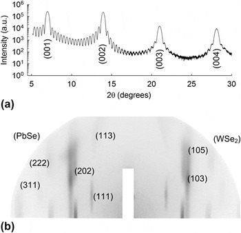
Inasmuch as it has a direct impact on the interpretation of electrical transport data, we first briefly discuss the unusual nanostructure present in our [(PbSe)0.99]1[WSe2]1 nanolaminates. The composition of this misfit-layered compound is characterized by an incommensurate, nonepitaxial relationship between the independent substructures of the two components, resulting in the PbSe:WSe2 ratio of 0.99:1. This is confirmed by both grazing incidence in-plane diffractionReference Zschack, Heideman, Mortensen, Nguyen, Smeller, Lin and Johnson15 and electron microprobe analysis.Reference Lin, Smeller, Heideman, Zschack, Koyano, Anderson, Kykyneshi, Keszler, Anderson and Johnson3 As a result of the artificial periodic structure created in the layered MER precursor, the [(PbSe)0.99]1[WSe2]1 specimens form with near-perfect texture, with the “c-axis” nanolaminate period normal to the substrate surface. This is evidenced by conventional laboratory powder XRD [Fig. 1(a)] from a [(PbSe)0.99]1[WSe2]1 specimen deposited on a <100> oriented silicon substrate, in which only (00l) reflections originating from the periodicity in the c-direction, i.e., perpendicular to the substrate surface, are observed. Kiessig fringes, originating from the interference of x-rays scattered from the top and bottom interfaces of the film, are observed to 2θ > 23°, indicating an extremely smooth film with deviations in thickness, i.e., roughness,Reference Wainfan and Parratt16 of ∼2 Å. Diffracted intensity collected using synchrotron x-ray radiation (energy of 12.50 keV) and an area detector [Fig. 1(b)] obtained with a fixed incident beam angle of θ = 0.6° further elucidates the nature of the layering and nanostructure. The features in these data can be attributed to the individual components separately, i.e., reflections are observed that can be indexed to the PbSe and WSe2 components, respectively. The breadth of mixed (hkl) reflections is characteristically much broader along the L direction, indicating a significantly shorter coherence length in this direction. These features are understood in terms of rotational (turbostratic) disorder, which results in little long-range order in these materials,Reference Zschack, Heideman, Mortensen, Nguyen, Smeller, Lin and Johnson15 in spite of the precise layering of the components which also exhibit a high degree of local ordering. This interpretation is supported by findings from high-resolution transmission electron microscopy studies, which confirm the interlayer disorder.Reference Lin, Smeller, Heideman, Zschack, Koyano, Anderson, Kykyneshi, Keszler, Anderson and Johnson3
(a) Laboratory thin film x-ray diffraction (XRD) pattern collected from a [(PbSe)0.99]1[WSe2]1 multilayer film. The low angle Kiessig fringes extend to 2θ > 23° indicative of highly uniform film thickness and layering. (b) Image plate data from synchrotron XRD.

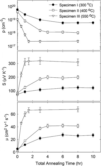
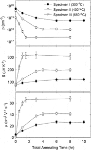
The effect of both annealing temperature and annealing time on the electrical transport properties of [(PbSe)0.99]1[WSe2]1 was investigated. The three [(PbSe)0.99]1[WSe2]1 specimens, I, II, and III, were annealed at 300, 400, and 550 °C, respectively. The effect of annealing time on room temperature carrier concentration, Seebeck coefficient, and Hall mobility, shown in Fig. 3, was investigated by measuring the electrical transport properties between successive anneals at fixed temperature. Since the detailed carrier characteristics and transport mechanisms are not yet well understood in turbostratic nanolaminates such as [(PbSe)0.99]1[WSe2]1, we use a simple model of a single carrier conductor to quantitatively evaluate the relative effects of annealing on the electrical transport properties. Carrier concentration, p, and Hall mobility, μ H, were estimated from the room temperature Hall coefficient R H = 1/(pe) and the expression μ H = R H/ρ, respectively, where |e| is the electron charge and ρ is the measured electrical resistivity. The Hall coefficient and Seebeck coefficient for all specimens were both positive, indicating holes are the majority carriers in these films, before and after the vapor annealing.
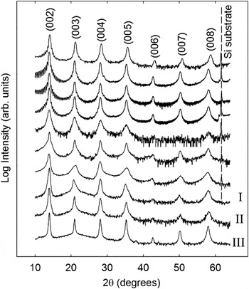
Typical electrical transport properties of [(PbSe)0.99]1 [WSe2]1 films evaluated after formation of the PbSe–WSe2 nanolaminates, i.e., after self-assembly by annealing at 400 °C under N2 but prior to Se vapor annealing. N2 anneal only, prevapor annealing, reveal relatively high hole concentration values (p > 1019 cm−3) for nominally undoped semiconductor films, consistent with a relatively high concentration of structural and/or compositional defects. The low temperature self-assembly process allows these two-component nanolaminates to be kinetically trapped in spite of their thermodynamic metastability. At the same time, nonequilibrium distributions of structural and compositional defects are presumably trapped as well, strongly influencing carrier transport. Prevapor annealed films also exhibit relatively low Hall mobilities, also likely the result of a high density of structural defects. Moreover, we have also observed a range of c-axis lattice parameters, from 12.66(1) to 12.80(1) Å, is possible for nominally [(PbSe)0.99]1[WSe2]1 specimens, suggesting a substantial phase width in which this compound can be prepared and sensitivity to the precise deposition conditions. In addition to the specimens I, II, and III that were investigated by vapor annealing, a number of other specimens of [(PbSe)0.99]1[WSe2]1 are included in Fig. 2 for comparison. Although the [(PbSe)0.99]1[WSe2]1 nanolaminates are readily reproducibly prepared, the relative intensities and peak breadths exhibit some variation, also likely resulting from a breadth in phase space within which the compound is formed.
Laboratory XRD data (intensity on log scale) collected on 10 different [(PbSe)0.99]1[WSe2]1 films from 10 different depositions, including the three specimens (I, II, III) that were investigated by vapor annealing. The broad background at lower angles in specimens I, II, and III originates from the fused silica substrates.

Before discussing the observed trends in the electrical transport properties, we first consider three potential effects the vapor annealing may have on the specimens, which might influence the measured transport properties: (i) Given the strong anisotropy in electrical properties expectedReference Wiegers4 to be present for [(PbSe)0.99]1[WSe2]1, changes in preferred orientation, i.e., texture, of these nanolaminates with annealing could affect the observed transport properties. (ii) The small (∼10 nm or less) in-plane PbSe and WSe2 component domain sizes might increase with annealing, influencing carrier mobility and possibly carrier concentration. (iii) Compositional and structural defects (possibly including the nature of domain boundaries at fixed domain size) are reduced with annealing. To explore the first possibility, rocking curve data were collected on the (003) reflection of a [(PbSe)0.99]1[WSe2]1 specimen annealed under selenium vapor at 400 °C as a function of annealing time. No appreciable difference in the rocking curve widths was detected after annealing under selenium vapor for 6 h, sufficient time for the electrical properties to reach a steady state as shown in Fig. 3. From these data, we conclude that changes in film texture are not measurably influenced by the vapor annealing process. To explore the second possibility, we analyzed XRD intensity data collected by scanning through mixed reflections of the components in reciprocal space along Q both perpendicular (e.g., along L) and parallel (e.g., along H) to the film surface. From the breadth of these profiles, the average domain size (coherence length) can be estimated.Reference Zschack, Heideman, Mortensen, Nguyen, Smeller, Lin and Johnson15 From these data, we found no significant change in domain size after annealing, which remained near ∼10 nm, suggesting the nanostructure and turbostratic disorder is retained after annealing. From these observations, we conclude that neither increase in texture nor increase in domain size is a likely source of the observed trends shown in Fig. 3. This suggests that changes in electrical transport properties upon annealing can be attributed to a decrease in other compositional and structural defects.
Hole concentration (p), Seebeck coefficient (S), and Hall mobility (μ H), of specimens I, II, and III, as a function of annealing time.

As shown in Fig. 3, the transport properties for all three specimens evolve monotonically with time, and after sufficient time plateau to values that do not change upon further annealing treatments. This suggests that a steady state in the film has been reached. The rate at which this steady state is obtained is clearly higher for higher annealing temperatures, consistent with the expected increase in the rate of mass transport that should occur at higher temperatures. The carrier concentration is substantially reduced for all three specimens as a result of the vapor annealing process. As expected from the decrease in carrier concentration, the Seebeck coefficient also increases substantially with annealing in each case; the largest value of the Seebeck coefficient of 310 μV·K−1 is observed for specimen I at a carrier concentration near 2 × 10Reference Qiu, Zhao, Steward, Dyck and Burda17 cm−3.
We have found the Hall mobility [Fig. 3] in these films shows remarkable enhancement after annealing under Se vapor, which is consistent with the decrease in carrier concentration and a decrease in defects as compared to the films before vapor annealing. In spite of the turbostratic disorder and resulting small average in-plane domain sizes of either component, on the order 10 nm or less, relatively high mobilities are observed in the postannealed specimens, exceeding 60 cm2 V−1·s−1 for specimen III annealed at 550 °C. Density functional theory calculations within the generalized gradient approximation have recently been carried out for [PbSe]n[WSe2]1 (n = 1, 2) commensurate approximate structures.Reference Zhang and Singh13 These calculations indicate that the electronic states near the valence band maximum are derived from states associated with PbSe in the [PbSe]1[WSe2]1 commensurate approximate. Based on this, we infer that the electrical transport in our p-type [(PbSe)0.99]1[WSe2]1 turbostratic nanolaminates is likely associated with the PbSe component. The relatively high mobilities may be understood in terms of the PbSe domain boundary orientations. In studies of nanocrystalline p-type PbSe thin films prepared by chemical bath deposition, Qiu et al.Reference Qiu, Zhao, Steward, Dyck and Burda17 found a strong dependence of carrier mobility on crystallographic orientation of the PbSe grains. Specifically, as the volume fraction of crystallites oriented with [200] perpendicular to the substrate increased, for fixed average grain size, the mobility was found to increase significantly, suggesting that favorable grain boundaries facilitating carrier transport are achieved in these orientations which minimize scattering of carriers. As with other misfit-layered compounds,Reference Wiegers4 the domains in the rock salt-like PbSe layers in our [(PbSe)0.99]1[WSe2]1 specimens are precisely orientated with [200] perpendicular to the substrate.Reference Lin, Heideman, Nguyen, Zschack, Chiritescu, Cahill and Johnson2 If the domain boundaries in the PbSe layers are similar in nature to bulk PbSe films, the orientation may facilitate relatively high carrier mobilities.
In addition to the dependence of time to steady state on annealing temperature, the data of Fig. 3 suggest that higher annealing temperatures also result in steady state values for μ H and p that are higher and lower, respectively. However, further annealing of specimen I at 550 °C and specimen III at 300 °C, each for 4 h, resulted in no appreciable change in the measured electrical transport properties. This suggests that initial characteristics of the precursor likely have a strong influence on the final steady state properties of the film after prolonged vapor annealing. For example, variation in the precise Pb:W ratio deposited in the precursor is not expected to be significantly changed by the postformation annealing and may significantly influence the electrical properties.
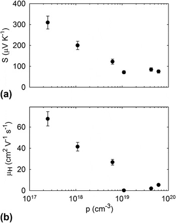
In Fig. 4, we plot μ H and S as a function of hole concentration, p, for the three specimens studied. Data are included only for specimens before the first vapor annealing step and after the last annealing step since it is conceivable that the specimens might not be homogeneous in the transient region before reaching the steady state. The data illustrate the wide variation in carrier concentrations and resulting Seebeck coefficients obtained in these nominally undoped specimens via vapor annealing alone. It is noteworthy that by applying the vapor annealing method, apparent carrier concentrations lower than 3 × 10Reference Qiu, Zhao, Steward, Dyck and Burda17 cm−3 can be achieved in [(PbSe)0.99]1[WSe2]1. An implication of this result is that meaningful doping studies in these films using methods such as ion implantation could be pursued.
(a) Seebeck coefficient and (b) Hall mobility as a function of hole concentration.

IV. CONCLUSIONS
We have investigated the effects of time and temperature during postformation vapor annealing of [(PbSe)0.99]1[WSe2]1 nanolaminates using bulk WSe2 as a source of selenium vapor. The use of a stoichiometric compound as the vapor source allows a controlled, reproducible annealing atmosphere. For the specimens studied, annealing was found to effectively reduce hole concentrations while simultaneously increasing Hall mobilities and Seebeck coefficients. The observed trends are consistent with the reduction of electrically active nonequilibrium compositional and structural defects in the films that are kinetically trapped during the low temperature self-assembly process. Approaches such as this may provide important postprocessing steps toward the goal of assessing the expected influence of nano-architecture in designed intergrowths and related nanostructured materials.
ACKNOWLEDGMENTS
The authors thank Ms. Jenia Karapetrova for technical assistance during collection of the synchrotron XRD data and acknowledge Dr. Harald Böttner for useful discussions concerning the vapor annealing apparatus. This work was supported through the Office of Naval Research (N0014-07-1-0358), the Oregon Nanoscience and Microtechnologies Institute, and the Army Research Laboratory. Coauthors C. Mortensen and C. Heideman were supported by the National Science Foundation through the Integrative Graduate Education and Research Traineeship (IGERT) (Grant No. DGE-0549503). The use of the APS was supported by the U.S. Department of Energy, Office of Science, Office of Basic Energy Sciences, under Contract No. DE-AC02-06CH11357.