


I. INTRODUCTION
Wireless communication systems are projected to be one of the fastest growing electronics industries in the next several years. Recent advances in integration technology and device performance demands higher packaging density from high-frequency integrated circuits (ICs). Flip-chip technology is emerging as a leading technology to meet the high-frequency and the high-density requirements [Reference Lee and Lee1]. Recent works have shown that it is suitable to integrate all circuits on GaAs microwave monolithic integrated circuit technologies in the millimeter wave frequency range. However, the low cost of silicon-based IC compared to GaAs makes silicon the process of choice in many radio frequency (RF) integrated circuit (RFIC) applications [Reference Niknejad and Meyer2]. Silicon-based RFIC requires integrated on-chip inductors as one of the key elements for voltage-controlled oscillator (VCO), low noise amplifiers, and single-chip transceivers. Silicon-based IC technologies have not been widely used with flip-chip technology for RF applications. Passive and active circuitries on flipped silicon chip face different coupling and parasitic mechanisms compared to the traditional wirebond package technology. Two major differences arise in the flip-chip technology compared to wirebond technique. First, the back plane of the flipped chip is no longer sitting on a solid ground plane but instead it is a floating ground. Second, the top of the die faces ground plane whereas wirebond faces away from ground plane. Several papers have addressed inductor performance on silicon substrate based on wirebond packaging technology since the introduction of inductor on silicon [Reference Nguyen and Meyer3, Reference Burghartz4]. Meanwhile, passive devices on flip-chip packaging technology are not studied extensively. On-chip inductors generally enhance the reliability and the efficiency of silicon-integrated RF cells and contribute to a higher level of integration. The limitation of inductors on flipped silicon chip should be clearly characterized and understood by the circuit designers in order to make appropriate design optimizations. Conventional on-wafer measurement techniques to characterize RF flip-chip face some difficulties because conventional on-wafer technique cannot characterize changed electric and magnetic field effects due to flip-chip configuration. The development of a characterization technique for flip-chip packages is motivated by the need to predict the behavior of devices in flipped environment at RF frequencies. In order to minimize the effect of the parasitics on flipped spiral inductor, the electromagnetic couplings as well as the neighboring bump effects from both chip and package substrate should be further analyzed and investigated.
In this paper, the effect of the flip-chip technology on the performance of on-chip silicon inductor is presented. Results from measurements and simulations are shown. It shows that the inductance of flipped on-chip spiral inductor on silicon substrate is affected by flip-chip environment. An on-strip technique was used to measure the RF performance of the flipped chip inductors. The on-strip measurement setup was further analyzed by using three-dimensional (3-D) full-wave electromagnetic simulation and experimentally validated up to 20 GHz by using vector network analyzer and on-wafer probe station. Assessment and characterization of a flipped on-chip spiral inductor is also presented as a validation of this technique. The organization of the paper is as follows: The difference between wirebond and flip-chip technology is reviewed in Section II. In this section, different electrical and magnetic behaviors on RF of flipped on-chip spiral inductor are shown. Section III explains the on-strip flip-chip measurement setup. Section IV discusses the effects of flip-chip technology on circuit performance and provides an equivalent circuit model for flipped on-chip spiral inductor. The S-parameters of the measured flipped spiral inductor is compared to those of the equivalent circuit model. The proximity effects between bump and inductor in flip-chip environment are studied in Section V.
II. ON-CHIP SPIRAL INDUCTOR IN FLIP-CHIP AND WIREBOND TECHNOLOGY
RFIC around 2 GHz has been successfully implemented using wirebond technology. However, flip-chip package provides a long-term potential alternative for significantly reducing package cost and system size using direct chip attach to PCB system boards. Flip-chip also stands to benefit from improved performance for RF, digital, and mixed signal applications in highly integrated chips [Reference Davis5]. Low impedance signal paths can be achieved from the inherent inductance drop of the two technologies (nHs' to pHs' in wirebond versus flip-chip). Flip-chip technology can furthermore draw size benefit from bumps instead of wirebonds for interconnections. Two major differences exist between flip-chip and wirebond technology. The back plane of the flipped chip is no longer a solid ground plane meanwhile the top of the chip faces ground plane instead. Figures 1(a) and 1(b) show the cross-section of an inductor using wirebond and flip-chip package technology, respectively [Reference Kim and Itoh6, Reference Lee, Megahed and De Flaviis7].
Cross-sectional view of spiral inductor in (a) wirebond and (b) flip-chip technology.

Conventional wirebond package technology usually relies on die attachment to the top of ground plane of the silicon substrate. In general, the location of the ground plane impacts the RF current return path since electric energy is coupled to the substrate through displacement of current. Displacement and conduction of currents into the substrate lead to the electromagnetic field losses in silicon substrate. Since loss and quality factor (Q) are related, it is desirable to quantify it. The Q of an inductor is defined as

Spiral inductors on silicon substrate suffer from several power dissipation mechanisms, which yield lower inductor Q. The resistance of metal trace causes a high series resistance, which limits the performance of the inductors at low frequencies, while the capacitive coupling to the lossy silicon substrate is responsible for the degradation of the Q at higher frequencies [Reference Koutsoyannopoulos and Papananos8]. For frequencies below 1 GHz, the skin effect is relatively small since the thickness of metal trace is typically comparable to the skin depth [Reference Zheng, Tripathi and Weisshaar9]. Above 2 GHz, however, the sheet resistance worsens as skin effect increases and electric energy is coupled to the substrate through displacement current. The substrate losses arise from the displacement current flowing through the oxide and conduction current to nearby grounds, either at the surface of the substrate or at the back plane of the substrate. Induced current flowing in the substrate furthermore causes substrate current due to the time-varying fields of the inductor. The time-varying fields are determined by the scalar and vector potentials [Reference Ramo, Whinnery and Van Duzer10].


Using Maxwell's equations, the following equation is obtained:

The first term identifies the magnetically induced eddy currents in the substrate of the metal conductors. The second term represents the dynamic radiation current. The third term includes the electrically inducted conductive and displacement currents in the substrate. The quality factor is proportional to the net magnetic energy stored, which equals to the difference between the peak magnetic and electric energy for an inductor. Magnetic coupling is largely responsible for the degradation of the Q of on-chip inductor. Since the magnetic field induced by the eddy current in conductive material is orthogonal to the magnetic field, and the top of the chip faces the package substrate and ground in flip-chip as shown in Fig. 1(b), the Poynting's theorem can be used to calculate the total power crossing the surface enclosing the inductor trace. It can also be used to quantify the eddy current losses with magnetic vector potential. The complex Poynting's vector is given by

Poynting's vector is integrated over the surface y, the power crossing the substrate is obtained from

For the time-varying case, the real component of total power is due to the lossy substrate since no other loss mechanisms exist for spiral inductor in wirebond technology [Reference Tegopoulos and Kriezis11]. However, flipped on-chip spiral inductor creates eddy current in the package substrate and ground plane. The eddy current in the package substrate is a negative increasing function that represents decreasing inductance as a function of frequency. The inductance decreases as the eddy currents flow in the package substrate. The eddy currents in substrate flow in a direction opposite to the current on inductor trace and generate a magnetic field. This magnetic field tends to cancel the penetrating magnetic field of the inductor and decrease the effective inductance. This can be explained by Lenz's law. However, the eddy currents flowing in the package substrate can be ignored due to low conductivity of package substrate material. Figure 2(a) shows the measured inductance of wirebond and flip-chip inductor on lossy silicon substrate. The measured on-chip spiral inductor has the following geometrical characteristics: outer dimension of 160 µm by 160 µm, metal trace width of 10.7 µm, and metal spacing between traces of 2.1 µm. The metal traces are insulated from the silicon layers by a SiO2 layer having a thickness of 4.39 µm and a dielectric constant of 4.2. The lossy silicon substrate under the SiO2 is 271 µm thick. The measured flipped on-chip spiral inductor uses the same geometrical characteristics of the wirebond inductor with the exception of the presence of the backside metal. The measured flip-chip inductance includes bump height of 80 µm, underfill between package substrate and flipped inductor. Figure 2 shows measured inductance and Q-factor of wirebond and flip-chip on-chip spiral inductor. Figure 2(a) displays the effective inductance of the wirebond on-chip spiral inductor, which is similar to that of the flipped on-chip spiral inductor up to 4 GHz. However, the effective inductance of the flipped on-chip spiral inductor shows peaking behavior around 6 GHz due to low self-resonance frequency (10.5 GHz). This difference can be explained by associated package structure. The flipped inductor has eddy current in package substrate and parasitic capacitance due to flipped inductor facing package substrate and ground. As already mentioned, eddy current in package substrate can be ignored due to low conductivity of package substrate, while parasitic capacitance due to different ground plane of flipped inductor is significant. The resonance frequency for the flipped spiral inductor is lower than the wirebond spiral inductor due to the larger parasitics capacitance from 80 µm flip-chip height and dielectric constant of 3.8 underfill in the flip-chip structure. The Q of on-chip spiral inductors in different package is also affected by the associated package structure. The location of the ground plane impacts the RF current return path in flip-chip structure. The inductor RF current return path for flipped silicon substrate is associated with locations of ground substrate contacts that exist on the top surface of the chip. The changed RF current return path for flipped silicon substrate results in significant variations in current density and current distribution in the substrate. The changed current density and distribution cause variations in flipped inductor resistance and inductance at high frequencies. The measured Q of wirebond and flip-chip inductors are shown in Fig. 2(b). The Q of the flipped on-chip spiral inductor is lower than the wirebond on-chip spiral inductor due to lower effective inductance at low frequencies and higher parasitic capacitance at high frequencies as well as loss due to eddy current.
Measured (a) inductance and (b) quality factor of wirebond and flip-chip inductor.

III. ON-STRIP MEASUREMENT TECHNIQUE
RF flip-chip characterization setup using on-strip measurement method is shown in Fig. 3. The chip was mounted onto a package substrate to measure the electric and magnetic characteristics of the flipped on-chip spiral inductor. The transition structures from on-wafer measurement probe pads to on-chip spiral inductor on chip were fabricated on a low-cost package substrate to measure the high-frequency response of RF flip-chip. In this setup, on-wafer measurement was used to obtain scattering parameters of package-mounted flipped on-chip spiral inductor.
On-strip measurement structure.

A) Structure of on-strip measurement
Transitions between the ground-signal-ground (GSG) probe pads and the substrate vias are accomplished by using tapered coplanar waveguide (CPW) traces on the bottom of package substrate [Reference Chun, Pham, Laskar and Hutchison12]. The entire structure is designed to maintain 50 Ω characteristic impedance using tapered CPW transmission lines. Region I in Fig. 3 shows tapered transition structure between GSG probe pads and package vias. The designed GSG probe pads have the signal pad width of 120 µm and the space between signal and ground pads of 60 µm. GSG on-wafer pads structure satisfies the probe pitch of 150 µm. The metal space limitation comes from package process limitation at the time of design. The diameter of package vias is 300 µm. The minimum distance between vias is 75 µm. The CPW trace on the bottom of package substrate provides a transition between the pitch of the GSG probes used for on-wafer measurement (150 µm) and package vias. CPW traces between substrate vias and flip-chip bump are located on the package upper substrate and shown in Region II of Fig. 3. The test structure on chip is shown in Region III of Fig. 3. The total length of on-strip measurement structure is 6 mm. This transition structure was designed with tapered CPW transition to reduce discontinuity effects. The tapered CPW trace was optimized to reduce interconnection loss using electromagnetic simulator. A simplified flip-chip test structure shown in Fig. 4(a) was analyzed using a 3D electromagnetic simulator. Advanced design system was used to design and optimize the CPW probe pad. Via pads under and on package substrate were designed according to the manufacturing design rule. The bump pads on substrate and chip were designed to keep bump pitch of 225 µm. Figure 4(b) shows simulated insertion and return loss of chip-to-package transition structure up to 20 GHz.
(a) Simplified geometry and (b) simulated S-parameters of chip-to-package transition.

B) Measurement results
Figure 5(a) shows a picture of fabricated bottom structure of package substrate. This structure includes input and output ports and tapered CPW structure between GSG probe pads and substrate vias. Measurements were carried out with Cascade on-wafer probe station with GSG pattern probes using a HP8510C vector network analyzer. Short-Open-Load-Thru (SOLT) [Reference Imparato, Weller and Dunleavy13] calibration was performed from 0.1 to 20 GHz, using calibration standard structures. Since the parasitics of on-chip open can be represented by Y-parameter equivalent lumped elements, which are in parallel to the passive and active circuits, the S-parameters of on-chip spiral inductor can be de-embedded from the measured S-parameters using a combination of cascaded and Y-parameter techniques. The same inductors were simulated by a full-wave electromagnetic simulator to compare measurement and simulation results. Figures 5(a) and 5(b) show pictures of on-strip measurement structure and on-chip spiral inductor, respectively. The white circles are vias in package substrate. The black circles are bumps between package substrate and die. The transition from vias to bump is located on upper substrate. This transition also uses tapered CPW structure to reduce discontinuity effects. The characteristics of the materials are as follows: the package substrate height of 200 µm, the package substrate dielectric constant of 4.2, substrate loss having tan δ = 0.023 at f = 2 GHz, bump height of 80 µm, under fill dielectric constant of 3.8 and molding layer height of 900 µm and dielectric constant of 4.3. The spiral inductor on flipped chip is as follows: outer dimension of 160 µm by 160 µm, metal width of 10.7 µm, and metal spacing of 2.1 µm. The metal traces are insulated from the silicon layers by a silicon oxide layer of 4.39 µm thickness and a dielectric constant of 4.2. The lossy silicon substrate has 271 µm thickness and 8 Ω-cm resistivity. X-ray machine was used to see other structures in the molding material, such as substrate vias and transition structure on package and flip-chip bump.
Fabricated (a) chip-to-package transition and (b) on-chip spiral inductor.

The measured S-parameters with on-strip measurement structure and de-embedded S-parameters are shown in Fig. 6. The flip-chip package parasitics, which include bumps, vias, and tapered CPW, are required in de-embedding process in order to characterize the on-chip device. De-embedding technique was used to extract package parasitics from measured S-parameters of the flip-chip structure.
Measured S-parameters of on-chip spiral inductor with on-strip measurement structure.

The flip-chip package model can be simplified in circuit simulations to predict the electrical performance of the device in a RF flip-chip structure. The transmission line segments, including a tapered CPW trace on each side of the package substrate, are modeled using transmission line models in circuit simulator as shown in Fig. 7. Lumped LC circuits are used to model the bump interconnections and via interconnections inside the package substrate [Reference Arai, Sato, Yamada, Nagai and Fujishiro14]. An L-network is used to model via transition. In addition, π-network is used to model bump interconnections for flip-chip interconnections. In the LC circuits, the capacitance represents the effect of the overlapping metallization area between chip and package, while the inductance represents the self and mutual inductance of the bumps and vias. The equivalent circuit of on-strip measurement structure shown in Fig. 7 can be divided into four parts: (1) input port that includes chip/package transition structure; (2) output port that includes chip/package transition structure, (3) test fixture on chip that includes parasitic capacitances and inductances, and (4) passive or active device on chip.
Equivalent circuit for on-strip measurement structure.

The input and output transitions are defined by the S-parameters, S I and S O, respectively. The S-parameters (S Device) of the flipped device are obtained by applying the following S-parameter measurement methodology which is shown in Fig. 8.
(1) S Total is obtained by measuring the two-port S-parameters with flipped die and input/output structure.
(2) S I is obtained by measuring the two-port fixture S parameters with input structure only.
(3) S O is obtained by measuring the two-port fixture S parameters with output structure only.
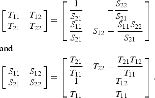
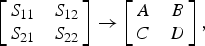
Determine the flipped device matrix S Device from S Total by applying the inverse chain scattering parameters or T parameter matrix multiplication techniques:

where conversions between S and T parameters [Reference Gonzalez15] are shown:
Simplified chip-to-package transition for de-embedding application.

The complex propagation constant and characteristic impedance are computed from the de-embedded S-parameters by using the following equations:

A three-step de-embedding method is followed to extract these package parasitics using simulated or measured S-parameters of the flip-chip device [Reference Cho and Burk16].
IV. EQUIVALENT CIRCUIT MODEL FOR FLIPPED ON-CHIP INDUCTOR
A small-signal equivalent circuit was extracted to understand the flip-chip effects of inductor parameters as shown in Fig. 9. In this circuit, R s includes a frequency-dependent term that is related to skin effect of metal and other high-frequency effects. C f models the parasitic capacitance that consists of the overlap capacitance between the spiral and the underpass, fringing capacitance between adjacent metal lines. C 1 and C 2 represent the capacitance between the metal layer and the grounded substrate. The equivalent circuit model can be represented as a three separate blocks such that a simplified two-port network is created [Reference Pozar17]. The model parameters are extracted by Y-parameters.
(a) Simplified two-port network and (b) the equivalent circuit for inductor.

The equivalent circuit model can also be determined by extracting component values from the measured Y-parameters. Each block of this network is extracted from the measured Y-parameters such that

Corresponding equivalent parameters and self-resonance frequency are calculated using equations (7) that are shown in Table 1.

Comparison of inductor characteristics for different package environment at 2 GHz.

The measured wirebond inductor has a outer dimension of 160 µm by 160 µm, a metal trace width of 10.7 µm, metal thickness of 3 µm, and metal spacing between traces of 2.1 µm. The measured flip-chip inductor uses the same geometrical characteristics of the wirebond inductor with the exception of the presence of the backside metal and bumps. Theses results show the increase of C 1, C 2, and C f in flip-chip environment. As a result, the self-resonance frequency is decreased with increased parasitic capacitance. This result can be understood because flipped on-chip spiral inductor faces package substrate and ground. In addition, the increase of R s with flip-chip can be observed in Table 1. The location of the ground plane impacts the RF current return path since electric energy is coupled to the substrate through displacement current. The RF current return path is concentrated on the surface of silicon layer with floating ground because the backside of the die is no longer grounded. Figure 10 shows the equivalent circuit model for a conventional on-chip spiral inductor and a flipped on-chip spiral inductor on package substrate [Reference Patrick Yue and Simon Wong18]. An equivalent model of flipped on-chip spiral is shown in Fig. 10(b). Parasitic capacitances (C 1 and C 2) of a flip-chip equivalent circuit are divided as C chip and C package. The C package represents the parasitic capacitance between spiral inductor and package substrate. The C package can be affected by different bump height or property of under-fill material. Accurate representation of the circuit is then obtained by minimizing the mean squared error between the Y-parameters and the admittance of each block over the entire frequency range of measured data. To assess the validity of the equivalent circuit models, S-parameter simulation and measurement were carried out as well. Two-port S-parameters were measured instead of a one-port parameter to allow extraction of parasitics from flipped structure. The equivalent circuit model of flipped spiral inductor consists of the equivalent circuit model of spiral inductor and the capacitance for flipped structure.
Equivalent circuit models for spiral inductor on (a) wirebond and (b) flip-chip.

The measured S-parameters of spiral inductor are with the simulated S-parameters to demonstrate the validity of the model in Fig. 11. When the measured and modeled equivalent circuit S-parameters are compared, good agreements are shown for the cases of wirebond spiral inductor and flipped spiral inductor. Good conformity between the two sets of S-parameter data confirms the validity of our model for the accurate estimation of the flipped spiral inductor model.
Equivalent circuit models for spiral inductor on (a) wirebond and (b) flipped structure.

V. BUMP PROXIMITY EFFECTS
The electrical performance of the complete flip-chip assembled structure cannot be derived by a simple combination of the individual characteristics of each element due to the electromagnetic coupling effect between each element and bump. Accurate estimation of the bump effect in the circuit is one of the main design objectives in flip-chip environment. One key circuit block of RFIC is the VCO blocks, which include an LC tank. To obtain low phase-noise performance, the existence of a high-quality LC resonator of the VCO is required. The Q of the resonator circuit is dominated by the quality factor of the on-chip inductor; hence, the design of such tank circuits is of major importance [Reference Burghartz, Edelstein, Soyuer, Ainspan and Jenkins19]. In LC tank circuits, the capacitance can be adjusted to tune the resonator frequency. However, the inductance and quality factor of flipped inductor are influenced by flip-chip structure. Figure 12(a) depicts the implementation of signal and ground bumps. The top metal layer can be used for die bump pad, which provides the shortest path to ground in flip-chip environment. The bump proximity effects cannot be ignored in the high-frequency circuit design. Conventional wirebond technology use peripheral pads for wire bonding, which is shown in Fig. 12(b).
Fabricated RFIC with (a) flip-chip and (b) wirebond technology.

The proximity effects of physical separation between inductor and neighboring bump was simulated and measured to examine how the isolation between them varies as the distance between them changes. A 3-D field analysis was used to perform electromagnetic simulation. The structure in Fig. 13(a) was simulated up to 20 GHz. For proximity effects, an RF signal is applied to port 1, while port 2 was connected to 50 Ω to measure output signal and port 3 is sensed to measure the coupled signal. The circled structure of Fig. 13(b) shows the three-port measurement structure under package substrate.
Three pairs of identical spiral inductor and bumps were simulated to examine the isolation (S 31) between inductor and bumps. The results in Fig. 14 suggest that the isolation between spiral inductor and bump is improved by the increased gap distance between inductor and bump.
Three-port structure for (a) electromagnetic simulation and (b) on-strip measurement.

Simulated S-parameters for bump proximity effects.

Figure 15 depicts the measured inductance and quality factor with bump proximity effects. At low frequencies, similar inductances are obtained regardless of the technology used. There is no difference in inductance of flipped inductors with and without bump proximity effect. However above 4 GHz, the effective inductance of the inductor with bump proximity is larger than that of the inductor without bump proximity. Since the inductor is orthogonal with bump, mutual inductance between inductor and bump is not significant. By considering the definition of effective inductance, which includes the parasitic capacitance term, it can be noticed that the capacitance contribution is getting significant as frequency approaches its self-resonance frequency. The self-resonance frequency of the inductor with bump proximity is lower than that of the inductor without bump proximity. The variation of self-resonance frequency is explained by the coupling capacitance effects between bump and on-chip inductor.
Measured (a) inductance and (b) quality factor with bump proximity effect.

VI. CONCLUSION
Silicon-based inductors in flip-chip technology are analyzed using full-wave electromagnetic simulation and the laboratory measurement. The results show that the inductance of flipped on-chip spiral inductor is influenced by flip-chip environment. The changed RF current return path for flipped silicon substrate results in significant variations in current density and current distribution in substrate. The changed current density and distribution cause variations in flipped inductor resistance and inductance at high frequencies. The equivalent circuit model of the flipped inductor is verified with measured results over a wide frequency range. The RF flip-chip characterization technique using on-strip measurement method is presented. The transition structures of CPW probes are fabricated on a low-cost package substrate to measure the high-frequency response of RF flip-chip. The application of this method is demonstrated experimentally and theoretically up to 20 GHz. Based on these studies, the proper range of flip-chip parameters to obtain a maximum value of quality factor and self-resonance frequency for designing the optimal structure for RFIC's applications can be determined.
 Gye-An Lee received the B.S. and M.S. degrees in Electrical Engineering from Ajou University, Suwon, South Korea, and the Ph.D. degree in Electrical Engineering from the University of California, Irvine, in 2004. In 2000, he was an RF engineer with Motorola in the area of cellular wireless systems design. He is currently with Skyworks Solutions Inc., Cedar rapids, IA working on GSM/WCDMA Power amplifier design as staff electrical engineer. His research and work interests include RF power amplifier using System-in-a-package (SIP), RF and microwave passive and active circuits and components, RF and microwave characterization and testing techniques, and broadband smart antenna system design.
 Darioush Agahi is an independent consultant in the Wireless RF Systems space, however at the time this manuscript worked on he was a Senior Director of RF systems engineering at Skyworks Solutions Inc. in Irvine CA. Darioush received his B.S. in Electronics (1981) and M.S. in Medical Engineering from the George Washington University in Washington DC (1983). Also he received an MSEE from Illinois Institute of Technology in Chicago Illinois (1993) and an MBA from the National University in 1997. Darioush holds 21 US patents plus he is a Professional Engineer (P.E.) registered in the state of Wisconsin.
 Franco De Flaviis received the Italy degree (laurea) in Electronics Engineering from the University of Ancona, Ancona, Italy, in 1990 and the M.S. and Ph.D. degrees in Electrical Engineering from the University of California, Los Angeles (UCLA), in 1994 and 1997, respectively. In 1991, he was an Engineer with Alcatel as a researcher specializing in the area of microwave mixer design. In 1992, he was a visiting researcher at UCLA working on low intermodulation mixers. He is currently an associate professor with the Department of Electrical Engineering and Computer Science, University of California, Irvine. He has authored and coauthored over 100 papers in reference journals and conference proceedings, filed several international patents, and authored three book chapters. His research interests include the development of microelectro mechanical systems (MEMS) for RF applications fabricated on unconventional substrates such as printed circuit board and microwave laminates with particular emphasis on reconfigurable antenna systems. He is also active in the research field of highly integrated packaging for RF and wireless applications. Prof. De Flaviis is a member of the URSI Commission B.



