Introduction
Microstrip antenna (MSA) finds many applications in wireless systems, attributed to their advantages like low profile, planar design [Reference Kumar and Ray1]. The MSA bandwidth (BW) is increased by employing a lower dielectric constant thicker substrate [Reference Kumar and Ray1, Reference Wong2]. However, probe inductance limits the BW in thicker substrate antennas. In such designs, modified feeding techniques are employed, and among them, proximity feeding is the simplest method [Reference Herscovici3, Reference Kovitz and Rahmat4]. While maintaining the single patch configuration, the MSA BW is increased by employing the resonant slot [Reference Wong and Hsu5–Reference Radavaram and Pour10]. In coaxially fed wideband slot cut MSAs, substrate thickness greater than 0.06λc is needed, which increases the antenna volume. Here, λc refers to the wavelength at the center frequency of the reflection coefficient (S11) BW. For substrate thickness greater than 0.08λc, BW in slot cut MSA is increased by employing the proximity feed [Reference Deshmukh and Ray11, Reference Deshmukh and Ray12]. The thinner substrate design employing a resonant slot is reported but it requires dual feeds with a differential feeding [Reference Radavaram and Pour10]. A thinner substrate slot cut antennas employing a modified ground plane profile are reported [Reference Deshmukh, Chavali and Ambekar13, Reference Deshmukh, Ambekar and Chavali14]. They yield BW in excess of 25%, on a substrate thickness in the range of 0.04–0.06λc. However, these designs have lower peak gain attributed to the increased back-lobe radiation. Thinner substrate modified ground plane designs offering BW in excess of 70% are reported [Reference Mondal and Sarkar15–Reference Mondal and Sarkar17]. But these configurations employ modifications in the patch and the ground plane, thus leading to a complex design. While using a printed circuit element placed below the E-shape MSA, a wideband design on a thinner substrate is obtained [Reference Chen, Yang and Nie18]. This design offers 8% BW, but details about the design of the printed element are not discussed.
In this paper, wideband designs of proximity fed rectangular MSA (RMSA) on a thinner substrate, by employing printed Ring shape or C-shape resonators placed below the patch, are proposed. A technique of non-contact proximity feeding has been reported in the literature to enhance the BW in conventional and slot cut patches. But it requires substrate thickness > 0.07λc. On a thinner substrate, the capacitive impedance offered by the feeding strip limits the MSA BW. This paper presents a technique that achieves BW improvement on a thinner substrate, while considering the proximity feeding. The initial study in this paper highlights the limitation of the proximity feeding technique to achieve maximum BW, against a reduction in the substrate thickness. To achieve a BW improvement on a thinner substrate, proximity fed RMSA is loaded with either an open-loop printed Ring shape resonator or C-shape resonator. Resonators are present below the patch, thereby not increasing the antenna dimensions. An improvement in the BW is achieved through the coupling between the TM10 mode on RMSA and TM20r modes on printed resonators. The proximity fed RMSA designs individually loaded with Ring shape resonator or C-shape resonator elements are discussed. Among all, the design consisting of three C-shape resonators achieves maximum BW. On a total substrate thickness of 0.053λc, the antenna offers a simulated BW of 214 MHz (23.62%) with a broadside gain of greater than 6 dBi. Considering the substrate thickness, the results achieved in terms of BW and gain are improved ones against the reported wideband designs offering broadside radiation characteristics. Also, the proposed work puts forward a technique to increase the BW in proximity fed designs, while employing a thinner substrate. To highlight the novelty aspect, a detailed tabular comparison against the reported MSAs is discussed ahead in the paper. With the obtained antenna characteristics, the proposed wideband design can find applications in the GSM band (800–1000 MHz). The antennas proposed in this paper are initially optimized using CST software [19] followed by an experimental verification. In the reflection coefficient (S11) BW, radiation pattern and broadside gain measurements, ZVH–8, SMB 100A, FSC6 are used. The measurement is carried out inside the Antenna Laboratory in which wideband high-gain Horn antennas were used as the reference antennas. A good agreement is obtained between the simulated and the measured results.
Wideband proximity fed RMSA loaded with printed ring shape resonator
Wideband configuration of proximity fed RMSA loaded with printed open Ring shape resonator is shown in Fig. 1(a, b). Initially, rectangular patch is designed for the TM10 mode frequency of 875 MHz, using air-suspended FR4 substrate (h = 0.16 cm, εr = 4.3), with an air gap (ha) of 2.7 cm; thus realizing total substrate thickness of the antenna as 2.86 cm (0.085λg10). The λg10 refers to the wavelength at the TM10 mode frequency. The RMSA dimensions are calculated as, L = 13 cm and W = 15 cm. RMSA is fed using a square proximity strip of length “ls” = 2.2 cm, placed at a substrate thickness of “hs” = 2.5 cm above the ground plane and at a feed position of “xf” = 3.5 cm from the patch center. In the proximity feed design, electromagnetic coupling arising from the fringing fields of the strip excites the resonant mode on the patch that yields simulated S11 BW of 174 MHz (20.2%). The BW obtained is a function of proximity strip parameters, i.e. strip length and its thickness above the ground plane. To assess the effects of air gap and the proximity feed thickness, parametric study for the decrease in the total substrate thickness is carried out and smith chart for the same is provided in Fig. 1(c).
(a, b) Proximity fed RMSA loaded with resonant Ring shape loop, and (c) effect of reducing the substrate thickness on the S11 BW in proximity fed RMSA.

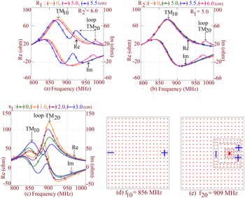
In each variation, the air gap thickness is reduced, and subsequently strip thickness is lowered. In equivalent circuit form, the proximity strip in combination with the probe inductance provides a series combination of inductor and capacitor [Reference Kumar and Ray1]. Against the decrease in the substrate thickness, probe inductance reduces, thus making the capacitive effect more dominant. With this for smaller hs, the loop formed does not lie completely inside VSWR = 2 circle, thereby reducing the S11 BW. As noted from Fig. 1(c), this effect is prominent for substrate thickness less than 0.07λg10. In [Reference Chen, Yang and Nie18], one such technique to increase the BW in thinner substrate antennas using coaxial feed was discussed. But the method presented is complex, as no details about the design of the printed circuit element used to reduce the thickness were elaborated. To enhance the BW on thinner substrate, while using the proximity strip, two techniques are presented in this work, which are simpler in design and implementation. In the first such design, printed Ring shape resonator loop is coupled with the proximity fed RMSA as shown in Fig. 1(a). The printed loop is placed below the rectangular patch, thus not increasing the overall patch size. The RMSA dimensions are maintained the same as specified earlier, while air thickness is chosen as “ha” = 1.6 cm, making the total substrate thickness of the antenna as 1.76 cm (0.053λg10). The RMSA is fed using a square proximity strip of side length “ls” = 2 cm, which is placed at “hs” = 1.5 and “xf” = 3.5 cm. For these substrate parameters, RMSA offers simulated BW of 80 MHz (9%), which is lower than that observed above in thicker substrate design. To analyze the effects of printed Ring shape loop dimension, parametric variations are carried out and resonance curve plots showing the variations in real and imaginary part of input impedance against variation in Ring dimensions “R1,” “R2,” and its position “x1” for a given width “wr,” are shown in Fig. 2(a–c).
Resonance curve plots for the variation in (a) “R1,” (b) “R2,” (c) “x1,” and (d, e) surface current distributions of proximity fed RMSA loaded with Ring shape resonator.

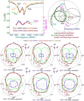
In the resonance curve two modes are observed. To identify the modes, surface current distribution at them was studied, as provided in Fig. 2(d, e). The first mode corresponds to TM10 mode. At the second mode, currents exhibit two half wavelength variation along the total Ring shape length. With this variation, resonant mode in Ring shape resonator is referred to as TM20r, also represented as “loop TM20” in Fig. 2(a–c). With the variation in lengths R1, R2 that constitutes a total Ring shape length, frequency of TM20r mode reduces, and it gets tuned with respect to the TM10 mode frequency of the RMSA. For the wideband response, impedance tuning at the two modes is also needed. Here, position of Ring shape resonator (x1) from the RMSA center optimizes the impedance at two modes to achieve a wideband response. The antenna dimensions in the optimum wideband design are “R1” = 5.7, “R2” = 6.0, “wr” = 1.0, “wg” = 0.4, and “x1” = 3.0 cm, and their results are provided in Fig. 3(a). The simulated and measured S11 BW is 135 MHz (15.16%) and 137 MHz (15.47%), respectively. Antenna offers broadside radiation pattern across the entire BW as mentioned in Fig. 3(c–h), with cross-polar radiation level less than 15 dB as compared with the co-polar level. The E-plane of radiation is aligned along Φ = 00. Antenna gain over the S11 BW is more than 6 dBi with a maximum value of 8.1 dBi. With reference to the TM10 mode frequency of RMSA, above mentioned BW is obtained for substrate thickness of 1.76 cm, i.e. 0.053λg10.
(a) S11 BW and gain plots, (b) smith chart for the optimum design, and (c–h) radiation pattern plots over the S11 BW for proximity fed RMSA loaded with Ring shape resonator.

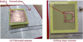
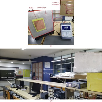
For the same substrate thickness, impedance locus plots for proximity fed RMSA and that loaded with a Ring shape resonator loop are provided in Fig. 3(b). For RMSA, loop is not formed inside VSWR = 2 circle. This does not yield maximum BW. But when RMSA is loaded with a Ring shape resonator then an additional loop due to the TM20r mode is formed inside the VSWR = 2 circle that increases the BW by 6%, on a thinner substrate, while using the proximity feed. Fabricated antenna showing RMSA and Ring shape resonator is provided in Fig. 4(a, b).
(a, b) Fabricated prototype of proximity fed RMSA loaded with Ring shape resonator.

Wideband proximity fed RMSA loaded with printed C-shape resonators
Design of proximity fed RMSA loaded with C-shape resonators is shown in Fig. 5(a–c). The C-shape resonators are placed below the patch and on the other side of FR4 substrate. Three variations of the design are investigated. First one with single C-shape resonator, followed by two and three resonators, each having different length Ri, where i = 2, 3 & 4. The vertical dimension R1 and resonator width wr is same across all the C-shape resonators.
(a, b) Proximity fed RMSA loaded with odd number of C-shape resonators, (c) even number, and (d) surface current distribution at TM20r mode on C-shape resonator.

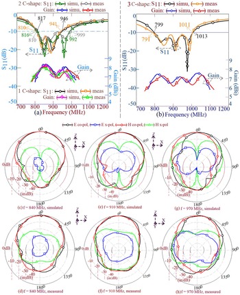
The C-shape resonator is simpler in fabrication against the open Ring shape resonator. Furthermore, in the geometry of C-shape against the Ring shape resonator, surface currents at TM20r mode are larger in contribution along the length, as shown in Fig. 5(d), hence the same is selected. In each design, for ha = 1.6 cm, by employing parametric variations for the C-shape dimensions, an optimum S11 BW is obtained that results in the optimum spacing of TM20r modes with reference to the TM10 mode. Results for all the designs are provided in Figs. 6 and 7.
S11 BW and gain plots for proximity fed RMSA loaded with (a) one, two, (b) three C-shape resonators, and (c–h) radiation pattern plots over the S11 BW for proximity fed RMSA loaded with three C-shape resonators.

(a) S11 BW measurement setup and (b) gain measurement setup for proximity fed RMSA loaded with three C-shape resonators.

In the optimum design consisting of single C-shape resonator placed below the proximity fed RMSA, resonator dimensions are R1 = 4.4, R2 = 8.6, wr = 1.0, x1 = 2.45 cm. It offers simulated and measured S11 BW of 129 MHz (14.63%) and 131 MHz (14.96%), respectively.
The broadside antenna gain is more than 6 dBi over the complete BW with a maximum value of 8 dBi. A single C-shape resonator offers equivalent BW to that given by Ring shape resonator. The addition of second C-shape resonator adds to another TM20r resonant mode and its optimum spacing with respect to RMSA’s TM10 and C-shape TM20r modes, yields increment in the BW. An optimum response is obtained for R1 = 4.4, R2 = 8.6, R3 = 7.2, wr = 1.0, y = 3.0 cm, and corresponding simulated and measured S11 BW are 176 MHz (19.47%) and 189 MHz (20.89%), respectively. The antenna offers similar broadside gain characteristics to that offered in single C-shape resonator design. A single and dual C-shape resonator designs offer broadside radiation pattern across the BW with E-plane aligned along ϕ = 00. The cross-polar level remains below 15 dB as compared with the co-polar level of radiation. An increment in the BW is further achieved by employing three C-shape resonators of unequal dimensions. The dimensions (Ri) of the individual resonator are kept different to achieve maximum BW. Here, while employing parametric study in each resonator lengths, optimum BW is obtained. For the three C-shape resonator dimensions as, R1 = 4.4, “R2” = 8.6, R3 = 7.2, R4 = 7.9, wr = 1.0, y1 = y2 = 5.0 cm, respective simulated and measured S11 BW are 214 MHz (23.62%) and 220 MHz (24.42%). The broadside antenna gain is more than 6 dBi across the S11 BW with a maximum value of 8 dBi. The radiation pattern across the BW is in the broadside direction with cross-polar level less than 15 dB as compared with the co-polar level. The E-plane of radiation is aligned along Φ = 00. On a total substrate thickness of 1.76 cm (0.053λg10), proximity fed RMSA yields simulated BW of 80 MHz (9%). Against these three C-shape resonators loaded proximity fed RMSA on the same substrate thickness offers nearly 15% increment in the S11 BW. Due to the capacitive impedance offered by the coupling proximity strip, BW in proximity fed RMSA on thinner substrate is less than 10%. The proximity feeding is the simplest method to enhance the MSA BW. In the literature, a simple technique to increase the BW of patch antenna employing proximity feed on thinner substrate showing broadside radiation characteristics, without using a modified ground plane structure, is not discussed. The proposed work addresses this research gap and presents a novel technique that employs printed resonators placed below the patch. This does not increase the patch size but provides S11 BW improvement on a substrate thickness of ∼ 0.05λc. This is the new contribution in the proposed wideband MSAs.
The S11 BW, broadside gain, and radiation pattern measurement setup are provided in Fig. 7. All these measurements are carried out inside the Antenna laboratory. The cable as seen in the S11 BW measurement is a low-loss cable. As the radiation pattern measurement is a relative plot of received power in the orthogonal planes, any amount of cable loss occurring has less effect. In the broadside gain and pattern measurement, reference wideband high-gain Horn antennas were used as the reference antennas. The RF source SMB 100A and spectrum analyzer FSC 6 are used in these measurements. A required minimum far-field distance calculated with reference to the highest frequency of the S11 BW is maintained between the reference Horn antenna and Antenna under test (AUT). Thus, for the obtained frequency results, minimum distance of 170 cm is needed. Around the measurement desk, minimum amount of metallic objects is present that ensures lower reflection from the surrounding objects. Also, the distance of the surrounding walls/objects is more than seven times the wavelength calculated with respect to lowest frequency of S11 BW. This gives path length of at least fourteen times the wavelength for any reflected wave coming from the surrounding objects. Due to this path length, reflected wave has lower effects against the direct wave present between the transmitter and receiver antenna. Broadside gain measurement is carried out using three-antenna method. This method is selected as it provides better accuracy for the measurements inside the laboratory. Also, it minimizes any loss or variations in the measurement due to the improper calibration of gain in the reference Horn antenna, as employed in the relative gain measurement employing single Horn antenna. These setup details provide fairly good measurements inside the antenna laboratory. The simulated radiation efficiency for the proposed designs was observed. Since the air-suspended FR4 substrate is employed, antenna radiation efficiency remains above 70% across the S11 BW.
To explain the wideband linear polarized radiation pattern response in proximity fed RMSA loaded with printed C-shape resonators, surface current distribution at the observed resonant modes in the optimum design of RMSA loaded with three C-shape resonators is studied, and its resonance curve plot and modal current distributions at the observed resonant peaks are shown in Fig. 8.
(a) Resonance curve plot and (b–e) surface current distribution at the observed resonant modes for proximity fed RMSA loaded with three C-shape resonators.

The surface current distribution at C-shape resonator mode is shown over the patch as well as over the C-shape resonator, i.e. the back view of the geometry. With three C-shape resonators, four resonant modes are present in the optimum design, i.e. for RMSA TM10 mode and TM20r mode in each C-shape resonator. At the resonance condition of TM10 mode, surface currents vary along the horizontal direction inside the rectangular patch, whereas at respective C-shape resonator mode, currents are showing two half wavelength variation along the C-shape length. This highlights a linear and horizontal variation of the modal currents over the antenna aperture across the resonant modes, which contribute to the S11 BW, and that achieves a broadside radiation pattern over the same. When the respective C-shape resonator mode is dominant then surface current over the rectangular patch is affected. This leads to some contribution of the vertical surface current components over the rectangular patch. These current components are the main source of variation in the broadside gain by around 1–1.5 dBi over the S11 BW, as observed in the above gain plots for the optimum designs.
Comparative analysis for the proposed design
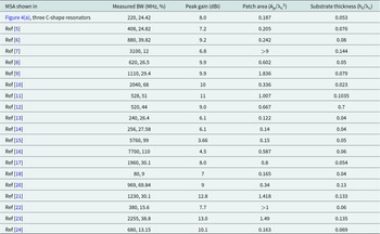
To highlight the novelty in the proposed study, a comparative analysis of the proposed optimum design against the reported wideband configurations is presented in this section. Among the proposed designs, RMSA loaded with three C-shape resonators provides maximum S11 BW for a smaller substrate thickness. Hence, a comparison of the same against the reported wideband MSAs is tabulated in Table 1 and is discussed below. The comparison is presented for measured S11 BW and gain against the antenna thickness and patch area. The substrate thickness (ht) mentioned in Table 1 is normalized with respect to the wavelength (λc), whereas patch area (Ap) is normalized with reference to the square of the wavelength (λc2) at the center frequency of S11 BW (fc). This normalization helps in comparing different configurations optimized in different frequency bands and substrate thickness, on a common platform.
Comparison of the proposed optimum wideband design against the reported wideband MSAs

The original E-shape MSA design reported in [Reference Wong and Hsu5] offers comparable BW but requires thicker substrate. The multiple slots cut design discussed in [Reference Wei-Wen, Qiu-Hao, Meng, Wang and Xu6] offers large BW on thicker substrate. However, it displays variation in the broadside gain by more than 3 dBi across the S11 BW. This is attributed to the asymmetric placement of slots with respect to the patch center. The double U-slot cut design discussed in [Reference Fan, Jiang, Liu, Xiu, Lin and Xu7] offers lower BW for substrate thickness in excess of 0.1λc. The wideband design discussed in [Reference Liu, Wei, Gao, Wen, Luo, Rui and Liu8] offers equivalent value of the BW for the antenna volume but the design consists of modified patch shape, slots, shorting post, and the differential feed. These design features increase the design complexity. Wideband antenna presented in [Reference Feng, Zhang, Weng and Jiao9] requires large antenna volume. The dual U-slot cut design presented in [Reference Radavaram and Pour10] does offer wider BW on thinner substrate. But it requires differential feeding and dual feeds. The gap-coupled array designs employing proximity feed yield BW of around 50% [Reference Deshmukh and Ray11, Reference Deshmukh and Ray12], but it requires large antenna size and thicker substrate. The modified ground plane design offers equivalent BW on thinner substrate but they have lower peak gain; attributed to the increased back-lobe radiation [Reference Deshmukh, Chavali and Ambekar13, Reference Deshmukh, Ambekar and Chavali14]. The modified ground plane designs discussed in [Reference Mondal and Sarkar15, Reference Baudha and Yadav16] offer very large BW or those discussed in [Reference Mondal and Sarkar17] provide comparable values of BW and gain against the proposed design. However, in these designs, an explanation about the resonant modes in the structure, which leads to a wider BW is not presented. Also, these designs employ modifications in the patch as well as ground plane thereby increasing the design complexity. Based on a similar technique as discussed in the proposed work, coaxially fed wideband design on thinner substrate is reported in [Reference Chen, Yang and Nie18] that employs printed circuit element positioned below the patch. This design offers lower BW against the proposed configuration. The proximity fed design discussed in [Reference Chavali and Deshmukh20] requires higher antenna thickness and employs multiple resonators placed around the fed patch. Against this proposed configuration is single resonator design optimized on a thinner substrate. The configuration discussed [Reference Wang, Xue and Xie21] employs array of four patches with a differential feeding. It offers higher BW and gain against the proposed design, but requires much higher antenna size. The multi-layer design discussed in [Reference Gao, Wang, Liu and Shaojun22] employs gap-coupled design involving half U-slot cut rectangular patch fed using the aperture coupled technique. This design requires larger patch size and offers lower BW against the proposed configuration. The antenna discussed in [Reference Shishkin Mikhail23] employs fed E-shape patch electromagnetically coupled with four rectangular resonators. This antenna offers higher BW and gain but overall antenna dimensions are very large. The design discussed in [Reference Jadhav, Rathod, Awale and Ray24] employs cavity backed configuration and offers higher broadside gain against the proposed design. Here, selection of cavity-backed design increases the antenna volume.
A gap-coupled multi-resonator technique is the simplest method among all the wideband techniques in MSA, since it just involves the placement of parasitic resonator in the immediate vicinity of the fed patch. Furthermore, proximity feeding is a simpler method to increase the MSA BW on thicker substrate and is widely reported in the literature. However, the proximity feeding has the limitation on thinner substrate due to a higher capacitive impedance offered by the feeding strip. In the reported papers, no techniques are discussed that consider the BW improvement on a thinner substrate while using the non-contact proximity feed. This paper presents a novel technique that provides BW increment on substrate thickness of around 0.05λc, while using a proximity strip. The proposed method works on a similar concept of multi-resonator gap-coupled design and thus is simpler in implementation and design, against the reported wideband techniques. In comparison to the reported work, the proposed study presents a novel technique using the proximity strip and coupled resonators that provides BW of 24% with a broadside radiation characteristics and a peak gain of 8 dBi, on a substrate thickness of 0.053λc. The addition of printed resonators does not increase the patch size and maintains a single patch wideband configuration. Against the reported configurations, the proposed design offers improved results in terms of S11 BW, gain, and substrate thickness, considered together. These are all the novelties in the proposed work against the reported configurations.
Conclusions
The proximity feeding is a widely reported and simplest technique to be used to enhance the MSA BW, but on a thicker substrate. But this method has limitations on a thinner substrates due to the higher capacitive impedance offered by the feeding strip. This paper puts forward a technique to increase the BW on thinner substrate, while using the proximity feeding and the rectangular patch. The parasitic Ring shape or C-shape resonators are placed below the patch, and thus they do not increase the antenna size. Among all the proposed configurations, the design employing three C-shape resonators offers the optimum result. It gives S11 BW of 24%, peak broadside gain of 8 dBi, but on substrate thickness of 0.053λc. With the obtained antenna characteristics, the proposed antenna can find applications in GSM 800–1000 MHz frequency band.
Data availability statement
No dataset was generated in the preparation of the manuscript.
Funding statements
No funds were received during the preparation of this manuscript.
Competing interests
Authors have no conflicts of interest/competing interests to disclose.

Venkata A. P. Chavali received BE degree in Electronics and Communication Engineering from Andhra University, Vishakhapatnam, India, in 2004, ME degree in Digital Communication from RGPV, Bhopal, India, in 2010, and PhD degree in Electronics and Telecommunication Engineering from D. J. Sanghvi College of Engineering, Mumbai University, in 2022. Currently, she is working as Assistant Professor with the Department of Electronics and Communication Engineering, Indian Institute of Information Technology Surat, Surat, Gujarat, India. Her research interest includes broadband microstrip antennas. She has 38 journals, 54 conference publications, 2 granted patents, and 1 monograph to her credit.

Amit Deshmukh received BE degree in Electronics from VIT, Pune University, and MTech and PhD degrees from the Department of Electrical Engineering, IIT Bombay. Currently, he is working as Professor & Head of the Department of Electronics and Telecommunication Engineering, D. J. Sanghvi College of Engineering, Vile-Parle (W), Mumbai, India. He has published more than 350 journal and conference papers, 4 patents, and 1 monograph.