
Recently, heterojunction solar cells based on p-type cuprous oxide (p-Cu2O) have been intensively studied[ Reference Minami, Nishi, Miyata and Nomoto 1 – Reference Hoye, Brandt, Ievskaya, Heffernan, Musselman, Buonassisi and MacManus-Driscoll 8 ] because of the difficulty of obtaining a suitable n-type Cu2O. We have recently reported that a conversion efficiency of 8.1% was achieved in heterojunction solar cells fabricated by inserting an n-type zinc-germanium-oxide (Zn1−XGeX-O) thin film between an Al-doped ZnO (AZO) thin film and a p-Cu2O sheet prepared with thermal oxidation,[ Reference Minami, Nishi and Miyata 9 ] whereas an efficiency only as high as 2% was obtained in heterojunction solar cells fabricated by depositing an AZO thin film on p-Cu2O sheets.[ Reference Minami, Nishi and Miyata 3 , Reference Minami, Miyata and Nishi 10 ] The efficiency enhancement that is associated with the insertion of an appropriate n-type oxide thin film is mainly attributed to the suppression of the recombination current that is caused by a large conduction band discontinuity at the interface between the AZO transparent electrode and the p-Cu2O sheet.[ Reference Minami, Nishi, Miyata and Nomoto 1 , Reference Minami, Nishi and Miyata 3 , Reference Minami, Miyata and Nishi 10 , Reference Minami, Nishi and Miyata 11 ] It should be noted that the recombination current at the AZO/p-Cu2O interface may also be suppressed by inserting an n-type or i-type Cu2O thin film between the AZO and p-Cu2O.[ Reference Minemoto, Matsui, Takakura, Hamakawa, Negami, Hashimoto, Uenoyama and Kitagawa 12 , Reference Takiguchi and Miyajima 13 ] Although the fabrication of p-n homojunction Cu2O solar cells using electrochemical deposition (ECD) have been reported,[ Reference Wang and Tao 14 – Reference McShane and Choi 17 ] the obtained maximum efficiency in p-n homojunction Cu2O solar cells is currently only 1.06%.[ Reference McShane and Choi 17 ] In contrast, Lee et al. have recently reported that an efficiency of 3.97% was obtained in a thin-film heterojunction solar cell fabricated by depositing an n-Ga2O3 thin film on a p-Cu2O thin film prepared using ECD.[ Reference Lee, Lee, Heo, Siah, Chua, Brandt, Kim, Mailoa, Buonassisi and Gordon 4 , Reference Lee, Chua, Brandt, Siah, Li, Mailoa, Lee, Gordon and Buonassisi 5 ] However, the obtained efficiencies in these thin-film heterojunction solar cells are always lower than those obtainable in heterojunction solar cells fabricated with the same structure on thermally oxidized p-Cu2O sheets, as described above.[ Reference Minami, Nishi, Miyata and Nomoto 1 , Reference Minami, Nishi and Miyata 3 – Reference Minami, Nishi and Miyata 6 , Reference Minami, Nishi and Miyata 9 ] This suggests that the crystallographical properties obtained in p-Cu2O and/or n-type Cu2O thin films prepared by ECD are currently insufficient for solar cell application, because the Cu2O thin films must be prepared on electrically conducting glass substrates coated with gold (Au) and/or transparent conducting oxide thin films. However, the crystallographical properties of Cu2O thin films prepared by ECD may be improved by epitaxially growing the thin films on high quality Cu2O substrates.
In this paper, we describe the epitaxial growth of undoped and manganese-doped Cu2O (Cu2O:Mn) thin films, using ECD, on high-quality p-type sodium-doped Cu2O (p-Cu2O:Na) sheets prepared by thermally oxidizing Cu sheets. By inserting an undoped or Cu2O:Mn thin film between the AZO and p-Cu2O:Na, a significant improvement of photovoltaic properties was achieved in AZO/undoped Cu2O/ or Cu2O:Mn/p-Cu2O:Na solar cells fabricated with a Cu2O homojunction.
Undoped (non-intentionally doped) Cu2O and Cu2O:Mn thin films were prepared on p-Cu2O:Na sheet substrates under various deposition conditions using the following ECD process.[ Reference McShane and Choi 17 ] Initially, an acetic acid and Copper (II) acetate aqueous solution was prepared with 0.08 M acetic acid, 0.02 M Copper (II) acetate and de-ionized water; then a 0.1–1.0 × 10⁻⁵ M manganese chloride (MnCl2) aqueous solution was added to the solution as a doping impurity; and after that, a 3 M lithium, sodium or potassium hydroxide (LiOH, NaOH or KOH) aqueous solution was added to adjust the pH to 4.9. Next, a p-Cu2O:Na sheet substrate was immersed in the above solution at a temperature of 70 °C; a Pt plate and the p-Cu2O:Na sheet substrate were used as the anode and cathode electrodes, respectively, of the ECD. Finally, the deposition was carried out under various current densities of 0.1–2.0 mA/cm2 for durations of 5–30 min. The ECD of n-type undoped Cu2O thin films reported by McShane and Choi was referenced for the above solution and deposition conditions.[ Reference McShane and Choi 17 ] The p-Cu2O:Na sheets were prepared by incorporating Na into Cu2O sheets prepared by thermally oxidizing Cu sheets, described elsewhere in detail.[ Reference Minami, Nishi and Miyata 6 , Reference Minami, Nishi and Miyata 18 ] In brief, the incorporation of Na into the oxidized Cu2O sheets, impregnated with NaCl powder, was carried out with a heat treatment at 700 °C for 1 h in an Ar gas atmosphere. Before being used as the substrate in the ECD, the p-Cu2O:Na sheets were always etched in three solutions: first, a solution of Iron (II) chloride and hydrochloric acid followed by a solution of nitric acid and sodium chloride and, finally, an ammonium persulfate solution. The Cu2O:Na sheets (thickness of 0.2 mm) used in this work were polycrystalline p-type semiconductors that exhibited a hole concentration on the order of 1015 cm−3 and a Hall mobility as high as 100 cm2/Vs. For comparison with these Cu2O:Na sheets, polycrystalline fluorine-doped SnO2 (FTO) coated glass sheets were also used as the substrate in the ECD. For device fabrication, AZO (Al2O3 content of 2 wt.%) thin films were prepared with a pulsed laser deposition (PLD), described elsewhere in detail.[ Reference Minami, Nishi, Miyata and Nomoto 1 , Reference Minami, Nishi and Miyata 3 , Reference Minami, Nishi and Miyata 9 – Reference Minami, Nishi and Miyata 11 ] The AZO thin films, functioning as the transparent electrode and prepared with a thickness of 200 nm, exhibited a resistivity on the order of 10−3 Ω.cm and a carrier concentration on the order of 1020 cm−3. The crystallographic properties were evaluated by x-ray diffraction (XRD) using an x-ray unit (Rigaku SmartLab) with a copper anode. The solar cells were fabricated by forming an AZO/undoped or Mn-doped Cu2O/p-Cu2O:Na structure on the front surface of the Cu2O:Na sheets and an Au ohmic electrode on the back surface. The photovoltaic properties of the Cu2O-based solar cells (electrode area of 3.14 mm2) were evaluated by exposing only the AZO transparent electrode area to AM1.5 G solar illumination (100 mW/cm2) at 25 °C.
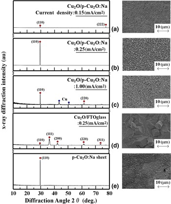
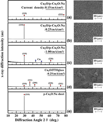
The resulting surface morphology and crystallographical properties in undoped (non-intentionally doped) and Mn-doped Cu2O thin films grown on p-Cu2O:Na sheet substrates by ECD were considerably affected by deposition conditions such as the pH and the amount of charge passed during deposition (current density and duration), whereas they were relatively independent of the kind of hydroxide used for adjusting the solution pH. The crystallographical properties of the Cu2O thin films grown on the p-Cu2O:Na sheet substrates were evaluated by a grazing-incidence XRD (GIXRD) analysis. Figure 1 shows typical GIXRD patterns and surface scanning electron microscopy (SEM) images of undoped Cu2O thin films grown on p-Cu2O:Na sheet substrates with a current density of (a) 0.15, (b) 0.25 and (c) 1.0 mA/cm2 by ECD. The undoped Cu2O thin films were deposited with a thickness of approximately 1 µm at a pH (adjusted using KOH) of 4.9 and a solution temperature of 70 °C. For comparison, the GIXRD pattern and surface SEM image of (d) an undoped Cu2O thin film grown on an FTO glass substrate and (e) a p-Cu2O:Na sheet substrate before the growth are also shown in Fig. 1. The undoped Cu2O thin film was grown on an FTO glass substrate at a current density of 0.25 mA/cm2 under the same deposition condition as used for the growth of the p-Cu2O:Na sheet substrates. As can be seen in Fig. 1, Cu was produced in the Cu2O thin films grown; the amount of Cu increased as the current density was increased above 0.25 mA/cm2. As evidenced from the GIXRD pattern, the obtained crystallinity (estimated by the full-width at half maximum (FWHM) of the (110) XRD peak) in undoped Cu2O thin films grown was strongly dependent on the current density. In addition to the above results, the obtainable crystallinity in undoped Cu2O thin films grown was investigated further by varying the current density near 0.25 mA/cm2 to obtain more detail, data not shown here. As a result, a current density of 0.25 mA/cm2 was found to result in higher quality crystallinity in undoped Cu2O thin films grown by ECD.
Typical GIXRD patterns and surface SEM images of undoped Cu2O thin films grown on p-Cu2O:Na sheet substrates with a current density of (a) 0.15, (b) 0.25 and (c) 1.0 mA/cm2 and (d) grown on an FTO coated glass substrate with a current density of 0.25 mA/cm2 by ECD; (e) a p-Cu2O:Na sheet substrate (before growth).

Note that the thermally oxidized p-Cu2O:Na sheets used as the substrate were polycrystalline with a grain size in the range from approximately 1 to 6 mm2. An undoped Cu2O thin film grown at a current density of 0.25 mA/cm2 exhibited the same grain structure as the p-Cu2O:Na sheet substrate used. As evidenced by the GIXRD patterns shown in Fig. 1, the undoped Cu2O thin film grown exhibited the same orientation as the p-Cu2O:Na sheet substrate. The crystallinity of undoped Cu2O thin films grown at a current density of 0.25 mA/cm2 was comparable with that of the p-Cu2O:Na sheet substrate. Namely, the FWHM estimated at the (110) GIXRD peak observed from the undoped Cu2O thin film grown at a current density of 0.25 mA/cm2 and the p-Cu2O:Na sheet substrate, as shown in Fig. 1(b) and (e), were 0.125° and 0.091°, respectively. In contrast, the FWHM of the undoped Cu2O thin film grown on a polycrystalline FTO substrate, as shown in Fig. 1(d), was 0.57°. In addition to the GIXRD analysis, we evaluated the crystallographical properties of the undoped Cu2O thin films grown on the p-Cu2O:Na sheet substrates with a current density of 0.25 mA/cm2 by ECD by in-plane XRD analysis and observed the (111) in-plane XRD peak from both the grown undoped Cu2O thin films and the p-Cu2O:Na sheet substrates (no data shown). As evidenced from the results mentioned above, it can be concluded that the undoped Cu2O thin film grown at a current density of 0.25 mA/cm2 by ECD had grown epitaxially on the p-Cu2O:Na sheet substrate; that is, an undoped Cu2O/p-Cu2O:Na homojunction was formed. It was also found that the current density dependence of crystallinity obtained in undoped Cu2O thin films grown under the same deposition condition as described above was not affected by Mn doping; the best current density was found to be 0.25 mA/cm2 for Cu2O:Mn thin films grown by ECD.
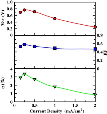
However, it was difficult to measure the electrical properties of the epitaxially grown Cu2O thin film in isolation when using ECD because of the necessity of using a conducting substrate such as the p-Cu2O:Na sheet or FTO. In particular, it is very difficult to only remove the epitaxially grown Cu2O thin film from an ECD-grown Cu2O/p-Cu2O:Na homojunction. Accordingly, Cu2O-based solar cells were fabricated by preparing a transparent AZO thin-film electrode on the ECD-grown Cu2O/p-Cu2O:Na homojunction using a PLD method to evaluate the suitability for photovoltaic applications. The obtained open circuit voltage (VOC), conversion efficiency (η) and fill factor (FF) as functions of current density are shown in Fig. 2 for the AZO/undoped Cu2O/Cu2O:Na homojunction solar cells fabricated with undoped Cu2O thin films grown on p-Cu2O:Na sheets by ECD with various current densities. The undoped Cu2O thin films were deposited with a thickness of approximately 240 nm at a pH (adjusted using KOH) of 4.9 and a solution temperature of 70 °C. We found that the obtained short-circuit current density (JSC) in AZO/undoped Cu2O/Cu2O:Na homojunction solar cells decreased slightly as the current density was increased from 0.15 to 2.0 mA/cm2, data not shown here. As can be seen in Fig. 2, the obtained VOC, η and FF increased as the current density was increased, reached a peak at 0.25 mA/cm2 and then decreased with a further increase of the current density. The current density dependence of VOC, η and FF may be related to that of the crystallinity of undoped Cu2O thin films, as shown in Fig. 1.
Obtained VOC, FF and η as functions of current density in homojunction solar cells fabricated with undoped Cu2O thin films grown on p-Cu2O:Na sheets with various current densities by ECD.

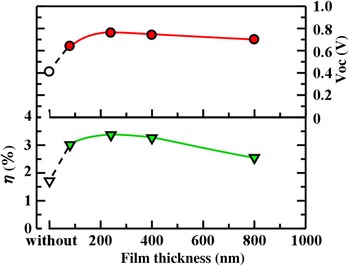
Obtained η and VOC as functions of film thickness are shown in Fig. 3 for AZO/undoped Cu2O/Cu2O:Na homojunction solar cells fabricated with undoped Cu2O thin films grown with various thicknesses under the optimized deposition condition on p-Cu2O:Na sheets by ECD. The undoped Cu2O thin films were deposited at a current density of 0.25 mA/cm2, a pH (adjusted using KOH) of 4.9 and a solution temperature of 70 °C. The η (open data point) plotted at the “without” mark on the horizontal axis represents the case of an AZO/Cu2O:Na solar cell (or fabricated with a film thickness of 0, i.e., without the ECD-grown undoped Cu2O thin-film layer). As can be seen in Fig. 3, the obtained η and VOC were increased dramatically by inserting an undoped Cu2O thin-film layer between the AZO thin film and the Cu2O:Na sheet; that is, η and VOC increased as the thickness of the undoped Cu2O thin film was increased up to 100–400 nm, and then decreased with a further increase of the thickness. The thickness dependence of η is mainly related to that of VOC. It should be noted that a high VOC of 0.76 V (η of 3.37%) was obtained in an AZO/undoped Cu2O/Cu2O:Na homojunction solar cell fabricated by inserting an undoped Cu2O thin film with a thickness of approximately 240 nm, whereas the VOC obtained in an AZO/Cu2O:Na solar cell was approximately 0.41 V (η of 1.71%). The significantly enhanced Voc and η suggest that the undoped Cu2O thin-film layer prepared by the ECD has excellent crystallinity as well as acts as an appropriate active layer. Consequently, the recombination current on the p-Cu2O:Na surface at the AZO/Cu2O:Na interface was suppressed by forming the undoped Cu2O/Cu2O:Na homojunction. In addition, the Fermi energy of the undoped Cu2O thin film, rather than that of the p-Cu2O:Na sheet, shifted toward the conduction band. However, it should be noted that when using ECD on p-Cu2O substrates, forming a Cu2O thin film that only exhibits n-type conduction is very difficult because the formed Cu2O p-n junction was reversely biased during the ECD process.
Obtained η and VOC as functions of film thickness in homojunction solar cells fabricated with undoped Cu2O thin films grown on p-Cu2O:Na sheets with various thicknesses.

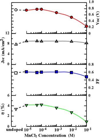
Because the Fermi energy of undoped Cu2O thin film is uncontrollable, obtaining a desirable Fermi energy would require further investigations to identify an effective donor in Cu2O.[ Reference Bai, Wang, Zhang and Tao 19 – Reference Meyer, Polity, Reppin, Becker, Hering, Kramm, Klar, Sander, Reindl, Heiliger, Heinemann, Müller, Ronning, Svensson, Pearton and Jagadish 22 ] Accordingly, we attempted to incorporate many kinds of impurities into undoped Cu2O thin films using the ECD method described above. As a result, we found that Mn doped into Cu2O may possibly act as an effective extrinsic donor. Obtained VOC, JSC, FF and η as functions of MnCl2 concentration are shown in Fig. 4 for AZO/Cu2O:Mn/Cu2O:Na homojunction solar cells fabricated by preparing Cu2O:Mn thin films on p-Cu2O:Na sheets using various levels of MnCl2 concentration in the ECD solution. The Cu2O:Mn thin films were deposited with a thickness of 240 nm at a current density of 0.25 mA/cm2, a pH (adjusted using KOH) of 4.9 and a solution temperature of 70 °C. The VOC, JSC, FF and η (open data points) plotted at the “undoped” mark on the horizontal axis represent the case of an AZO/undoped Cu2O/Cu2O:Na homojunction solar cell (or fabricated with a MnCl2 concentration of 0, i.e., an undoped Cu2O thin-film layer). As can be seen in Fig. 4, VOC, JSC, FF and η all increased as the MnCl2 concentration was increased to approximately 10−4 M. Note that η and VOC decreased significantly as the MnCl2 concentration was increased over approximately 10−4 M. Using a MnCl2 concentration of 10−4 M, the Mn content (Mn/(Mn + Cu) atomic ratio) in the Cu2O:Mn thin films was approximately 2.6 × 1019 cm−3 (0.51 at.%), as evidenced by x-ray photoelectron spectroscopy. It should be noted that a high η of 4.21% and a high VOC of 0.78 V were obtained in an AZO/Cu2O:Mn/Cu2O:Na homojunction solar cell fabricated by depositing a Cu2O:Mn thin film doped with a MnCl2 concentration of 10−4 M, i.e., without using an n-type semiconductor thin-film layer such as Ga2O3 or Zn1−XGeX-O.[ Reference Minami, Nishi and Miyata 3 , Reference Minami, Nishi and Miyata 9 ]
Obtained VOC, JSC, FF and η as functions of MnCl2 concentration in homojunction solar cells fabricated by preparing Cu2O:Mn thin films on p-Cu2O:Na sheets using ECD with various MnCl2 concentrations.

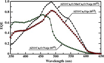
The external quantum efficiency (EQE) of various Cu2O-based solar cells was measured to estimate the p of the Cu2O active layer of the solar cells, because as we have reported previously the obtainable EQE wavelength dependence in Cu2O-based solar cells is dependent on the p of the p-Cu2O active layers used.[ Reference Minami, Nishi and Miyata 23 ] Fig. 5 shows typical EQE wavelength dependences for various Cu2O-based solar cells fabricated with AZO/Cu2O:Mn/Cu2O:Na and AZO/Cu2O:Na structures. The AZO/Cu2O:Mn/Cu2O:Na homojunction solar cell was fabricated by depositing a Cu2O:Mn thin film doped with a MnCl2 concentration of 10−4 M, as shown in Fig. 4. For comparison, AZO/Cu2O and AZO/Cu2O:Na solar cells were fabricated using Cu2O and Cu2O:Na sheets with p on the order of 1013 and 1015 cm−3, respectively, both without the inserted Cu2O thin-film layer. Note that the amount of EQE in the wavelength range from approximately 500 to 600 nm, near the absorption edge of Cu2O, decreased markedly as the p of the p-Cu2O sheets was increased. The blue-shift of the EQE wavelength dependence with an increase of the p, following the decrease of obtained η, is attributed mainly to a decrease of the width of the depletion layer created in these Cu2O thin films. Thus, the value of p of the Cu2O:Mn thin-film active layer is estimated to be less than 1013 cm−3, as seen in Fig. 5; that is, the Cu2O:Mn thin film doped with a MnCl2 concentration of 10−4 M by ECD is identified to be an i-type semiconductor. Consequently, the width of the depletion layer created in the AZO/Cu2O:Mn/Cu2O:Na homojunction solar cell fabricated by inserting an i-type Cu2O:Mn thin film is enhanced compared with that created in AZO/Cu2O:Na solar cells.
EQE wavelength dependences for AZO/Cu2O:Mn/Cu2O:Na homojunction, AZO/Cu2O and AZO/Cu2O:Na solar cells fabricated with a hole concentration (p), on the order of 1015 or 1013 cm−3, indicated in parentheses.

In summary, we described the epitaxial growth that results from preparing an undoped (non-intentionally doped) or Mn-doped Cu2O (Cu2O:Mn) thin film on thermally oxidized polycrystalline p-type sodium-doped Cu2O (p-Cu2O:Na) sheets using ECD. A significant improvement of photovoltaic properties was achieved in solar cells fabricated by inserting a manganese-doped Cu2O (Cu2O:Mn) thin film between an Al-doped ZnO (AZO) transparent electrode and p-Cu2O:Na sheets. The obtained photovoltaic properties in these solar cells, featuring a Cu2O:Mn/p-Cu2O:Na homojunction, were controlled by varying the content of Mn doped into the Cu2O:Mn thin film, achieved by varying the MnCl2 concentration of the ECD solution. An efficiency of 4.21% and an open circuit voltage of 0.78 V were obtained in an AZO/Cu2O:Mn/p-Cu2O:Na solar cell fabricated with a 240-nm-thick Cu2O:Mn thin film prepared with a MnCl2 concentration of 10−4 M. The ECD-grown Cu2O:Mn thin film was assigned as an i-type semiconductor.
Acknowledgments
The authors wish to acknowledge Mr. Y. Nishi, K. Fukuda, T. Nakagawa, K. Okumura, K. Yamada, T. Yoshida, K. Yoshimoto for their technical assistance in the experiments.