I. INTRODUCTION
Surface texturing in solar-based devices is a geometric method of reducing reflection in crystalline silicon substrates.Reference Chung, Chen and Chu1 It is often achieved by the anisotropic etching of (100)-oriented silicon substrates into square-based pyramidal structures.Reference Gee, Gordon and Laing2 The pyramidal structures are formed by the alkaline etching of (100)-oriented silicon surfaces along crystallographic orientations that expose the {111} planes.Reference Hylton, Burgers and Sinke3 Potassium hydroxide (KOH) and additive isopropyl alcohol (IPA) are two of the most common alkaline solutions that are used for anisotropic etching of silicon surfaces.Reference Tellier and Brahim-Bounab4–Reference Zubel and Kramkowska12 The sizes and uniformities of the resulting pyramids are also traceable to IPA, which acts as a wetting agent, when added to alkaline etchants.Reference Yang, Chen, Chiou and Lee11
Furthermore, the pyramidal sizes, heights, and base widths are usually on the order of several micrometers.Reference Zubel and Kramkowska12,Reference Moroz, Huang, Wijekoon and Tanner13 Hence, the reflection falls within a basic structure that supports geometric optics.Reference Zhu, Wang and Yang14 Consequently, the surface texturing of (100)-oriented silicon substrates can be used to improve the absorption of light within the silicon substrates.Reference Campbell and Green15 This can be achieved by using the reflection from micropyramids to redirect light to produce multiple reflections that increase the possibility of light absorption by silicon substrates. Since such increased absorption can enhance photocharge conversion and solar cell efficiency, there is a need to study the effects of micropyramidal geometries on the reflectance of textured silicon surfaces.
In a recent work, Baker-Finch and McIntoshReference Baker‐Finch and McIntosh16,Reference Baker‐Finch and McIntosh17 considered the reflection of normally incident light from textured silicon surfaces. They presented the reflection path and the fraction of rays that follow a given path, using geometrical approach for regular inverted pyramidal textures and a ray tracing method for random pyramidal textures.Reference Baker‐Finch and McIntosh16 They were able to establish that, for all normally incident rays that intersect a pyramidal facet, 88.9% of incident rays experience a secondary reflection, while the remaining 11.1% experience tertiary reflection.Reference Baker‐Finch and McIntosh17
However, in practice, the incident rays of sunlight are not always normal to the surfaces of textured silicon solar cells. Since the angles of incidence may vary, depending on the position on the earth, and the earth's rotation about the sun and about its own axis, there is a need to explore the possible effects of different angles of incidence on the reflection of sunlight from {111} facets on the surfaces of textured silicon solar cells. Hence, the work of Baker-Finch is limited to normal incidence, which is not always the case for most solar cells in service.
In this work, an analytical model is used to determine how incident light interacts with textured micropyramidal facets on alkali-textured silicon surfaces. The dependence of the secondary reflection on the angles of incidence of light rays is explored along with the contributions of the primary and secondary reflection to the total reflection. The possible optical interactions are considered for a range of pyramidal geometries and light incidence angles. The analytical model is then used to determine the reflectances of well controlled textured surfaces. The potential for light trapping is also explored, before discussing the implications of the results for the design of microtextured silicon surfaces.
II. MODELING
A. Pyramids on etched silicon surfaces
The silicon solar industry relies largely on silicon wafers with (100), (110), and (111) orientations.Reference O'Mara, Herring and Hunt18 However, (100) wafers are the most geometrically appealing, since the orientations of {111} planes can be easily located on them.Reference O'Mara, Herring and Hunt18 To understand the etching behavior of different wafers, it is important to know the relative positions of different crystal planes in these wafers. It is also important to know the angles that they make with each other, after etching.
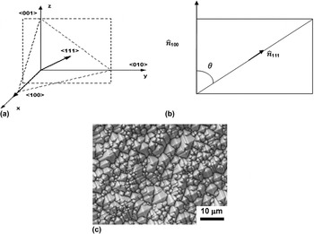
During wet anisotropic etching, grooves with {111} sidewalls are exposed.Reference Zhu, Wang and Yang14 These are aligned with {100} planes at specific angles.Reference Campbell and Green15 Also, the KOH solution is the preferred etchant that is used in the anisotropic etching of silicon to produce grooves with {111} sidewalls. This is attributed to its high anisotropy against {111} planes.Reference King and Buck19,Reference Parretta, Sarno, Tortora, Yakubu, Maddalena, Zhao and Wang20 Furthermore, the angles between the individual crystallographic planes can be calculated using vector operations (dot products), since the angles between {100} and {111} planes are the same as the angles between the unit vectors of their normals. Thus, by inspection, the unit normals of both the (100) plane and the (111) plane can be obtained from their Miller indices, as shown in Fig. 1.
(a) The square and triangular shapes represent the (100) plane and (111) plane, respectively, (b) a rectangle including the main diagonal of the cube used to determine the angle of interest, and (c) SEM image of pyramids on the surfaces of KOH etched (001) silicon wafers.

In an effort to demonstrate the geometrical properties of silicon crystal on a (100) plane, the dot product [Eq. (1)] is used to obtain the angle between the (111) plane indices and the (100) plane indices to be 54.74°.
 $${\hat n_{100}} \cdot {\hat n_{111}} = \left| {{{\hat n}_{100}}} \right|\left| {{{\hat n}_{111}}} \right|\cos \theta \quad ,$$
where  $\left| {{{\hat n}_{100}}} \right|$ and
 $\left| {{{\hat n}_{111}}} \right|$ represent the magnitudes of the unit normal vectors and θ is the angle between the (111) facet and the (100) substrate.
The above angle corresponds to that specified from Wulf's stereographic projections of a (100)-oriented silicon crystal.Reference Dziuban21 Due to symmetry of the (111) plane on the (100) plane, the (111) plane meets the (010) plane and the (001) plane at an angle of 54.74°. The intersection of the (111) plane also forms a square-based pyramid. This implies that, for all incident light rays normal to the substrate, the primary reflections are oriented at 54.74° to the substrate surfaces. However, for actual industrial c-Si solar cells, where non-ideal etching is observed, a slightly smaller base angle (or facet tilt angle) is normally observed.Reference Baker‐Finch and McIntosh16,Reference Baker-Finch22 This has been shown to be less than 52° in Refs. Reference Baker‐Finch and McIntosh16 and Reference Baker-Finch22.
B. Textured surface model
1. Vector geometry approach
For a collimated beam of light that interacts with a textured silicon surface at a particular angle,Reference Campbell and Green15 the vector geometry approach explored in this section considers the possible angles of incidence of light relative to the pyramidal {111} facets. Within this context, the vector geometry approach uses vector dot products and Phong's projection modelReference Geitz23 to determine the angles of the reflected rays.
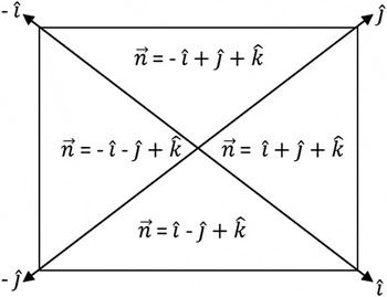
Since the KOH texturing of (100) wafers forms pyramidal {111} planes,Reference Wijekoon, Weidman, Paak and MacWilliams24,Reference Bressers, Kelly, Gardeniers and Elwenspoek25 we begin by representing the pyramidal surfaces by the vector coordinates of their plane normals. As shown in Fig. 2, the diagonals of the pyramids are represented, respectively, by unit vectors i and j, while k is the normal to the substrate. This allows us to specify the normal vector, n, for each of the facets on the pyramid (see Fig. 2).
Top-view of a square based pyramid showing the unit vectors and normal vectors on the textured surface.

Furthermore, the incident light ray is also defined by a vector, v = −i + j − x × k (where x is a variable). Since the normal to the substrate plane is the (001) direction, we define it as n = k. Thus, the dot product is used to determine the angle between v and n. This gives:
 $$v \cdot n = \left| v \right|\left| n \right|\cos \theta \quad ,$$
where |v| and |n| represent the magnitudes of the vectors v and n, respectively, and θ is the angle between v and n. Hence, rearranging Eq. (2) gives:
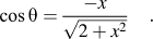 $$\cos \theta = {{ - x} \over {\sqrt {2 + {x^2}} }}\quad .$$
With the light ray vector, v, known for a given angle of incidence [Eq. (3)], the angles of incidence of the primary reflection can be determined. Note that Eq. (3) applies except when the incident angle is equal to 0°. When θ = 0°, the light ray vector is defined by v = −k.
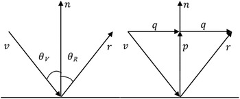
Once the incident light ray vector is known, the angles of the facets can be determined from Eq. (3). This makes it easier to obtain the secondary reflections. The coordinates of the reflected vector can be determined from the Phong's model.Reference Geitz23 Hence, the angle of incidence of the light reflected from a surface is equal to the angle of reflection, as shown in Fig. 3. If v is the direction of the incidence light ray vector, r is the direction of the reflected ray, n is the surface normal of the substrate, and θV and θR are the incidence and reflected angles, respectively, the reflected ray vector, r, can be determined from vector projection to be:
 $$p = v{{\left| n \right|} \over n}\quad .$$
Phong's reflection model showing the vector projection of the incidence light ray.

From Fig. 3, p is a projection of v onto n. Thus, we may rearrange Eq. (4) to obtain:
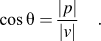 $$\cos \theta = {{\left| p \right|} \over {\left| v \right|}}\quad .$$
Also, using the dot product of two vectors, we may express cosθ as:
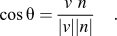 $$\cos \theta = {{v\,\,n} \over {\left| v \right|\left| n \right|}}\quad .$$
By combining Eqs. (4)–(6), p becomes
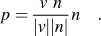 $$p = {{v\,\,n} \over {\left| v \right|\left| n \right|}}n\quad .$$
Since vector q connects v to its projection and also connects p to r, the coordinates of the reflected vector r are given by:
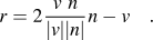 $$r = 2{{v\,\,n} \over {\left| v \right|\left| n \right|}}n - v\quad .$$
As an example, consider the case of light under normal incidence to the substrate, Eq. (8) can be used to calculate the secondary reflection for a given light ray (v = −k) that is incident to a facet with n 1 = i + j + k. The secondary reflection occurs on a neighboring facet with n 2 = −i – j + k. Thus, by combining Eqs. (6) and (8), 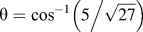 $\theta = \cos ^{ - 1} \left( {{5 \mathord{\left/ {\vphantom {5 {\sqrt {27} }}} \right. \kern-\nulldelimiterspace} {\sqrt {27} }}} \right)$, which is equal to 15.79°. This implies that, for normal incidence to a textured silicon (100) substrate, all secondary reflections occur at an angle of 15.79°.
The above method represents a possible approach to the determination of the angles between any incoming ray of light and any pyramidal facet. However, it does not treat cases in which fractions of the light rays are incident on different facets. Furthermore, the method does not determine whether reflection actually occurs or not. These issues can be addressed by exploring simpler systems, such as periodic two-dimensional (2D) arrangements of textured pyramids that will be considered in the next section.
2. 2D model of periodic pyramidal structures
a. Basic assumptions
A 2D model of a periodic pyramidal system is illustrated schematically in Fig. 4. This can be achieved in practice by masking the surface of a silicon wafer prior to the etching process.Reference Parretta, Sarno, Tortora, Yakubu, Maddalena, Zhao and Wang20 Assuming that the incident light rays are perpendicular to the surface of the substrate, the optical interaction of light (with the separate facets X and Y) can be idealized, as a two-dimensional problem.
The schematic diagram of the side view of a periodic pyramidal system.

In an effort to determine whether the angle of incidence, prior to the primary reflection on surface X, can produce secondary reflections, we gradually increase the angle of incidence from θ = 0° to θ = 35.3° until the incident light ray is tangential to facet Y (Fig. 4). Above 35.3°, the reflections from facet Y vanish until θ = 54.7°, at which the incident ray becomes normal to facet X. Furthermore, for incident angles greater than 54.7°, the reflected rays are directed away from the substrate and not toward it. Hence, secondary reflection will not occur for angles of incidence greater than 54.7°.
b. Contributing factors from primary, secondary, and total reflectances
To estimate the total reflectance, the fraction of light rays that is incident to each facet is estimated along with their contributions to the total reflectance. As shown in Fig. 4, angles θX and θY are the angles between the light ray and the normal vectors to facets X and Y, for primary reflections. Hence, the fraction of the light ray that falls on each facet can be expressed simply as the ratio of that angle's cosine to the sum of both angles' cosines. This is given by:
 $${F_{{\rm{X}}1}} = {{\cos \left( {{\theta _{\rm{X}}}} \right)} \over {\cos \left( {{\theta _{\rm{X}}}} \right) + \cos \left( {{\theta _{\rm{Y}}}} \right)}}\quad \!\!\!{F_{{\rm{Y}}1}} = {{\cos \left( {{\theta _{\rm{Y}}}} \right)} \over {\cos \left( {{\theta _{\rm{X}}}} \right) + \cos \left( {{\theta _{\rm{Y}}}} \right)}}\quad ,$$
where F X1 and F Y1 are the contributing factors of the primary reflections from facets X and Y, respectively. Since all of the reflections from facet Y vanish for angles greater that 35.3°, Eq. (9) is only valid for angles, θ, up to 35.3°. Beyond θ = 35.3°, F X1 = 1 and F Y1 = 0. For secondary reflections from facet Y, the fractional contributing factor, F Y2 = 1, since any light ray reflected from facet Y experiences a secondary reflection.
Unlike factor F Y2, the contributing factor (F X2) of the secondary reflections from facet X is more complex. By inspection, the contributing factor FX2 varies from 1 to 0, for four separate cases in the angle of incidence. In the first case, when the angle of incidence (to the substrate) is less than 19.4°, secondary reflection occurs on the neighboring Y facet, for all light rays that strike any arbitrary point on facet X. Secondly, for angles of incidence between 19.4° and 35.3°, some of the light rays reflected from facet X are directed away from the substrate, while those at angles of incidence between 35.3° and 54.7° are not able to strike some portion of facet X, due to shading from facet Y. Finally, at any angle greater than 54.7°, secondary reflections can no longer occur.
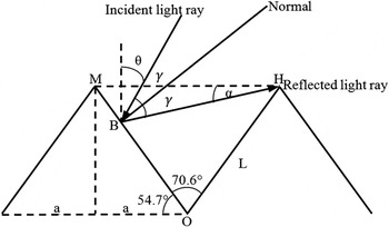
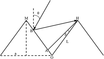
For any angle of incidence between 19.4° and 35.3°, as illustrated in Fig. 5, secondary reflection does not occur between points M and B on facet X (i.e., line length MB). Therefore, the fraction of facet X that does not produce secondary reflections from incident light rays is simply the ratio of the MB to MO. From Fig. 5, the base length of the pyramid is equal to the distance between the peaks of the two pyramids. This implies that MH is twice the line length, a, shown in Fig. 5. Hence, the line length, a, can be related to the side length, L, via the following expression:
 $$a = L\cos \theta \quad .$$
Light interaction with the pyramid facet at an angle between 19.4° and 35.3°.

Hence, for θ = 54.7°, Eq. (10) gives  $a = L\cos \left( {54.7} \right) = {L \mathord{\left/ {\vphantom {L {\sqrt 3 }}} \right. \kern-\nulldelimiterspace} {\sqrt 3 }}$.
Since MH is twice the length of the line segment, a, MH is now given by:
 $${\rm{MH}} = 2a = {{2L} \mathord{\left/ {\vphantom {{2L} {\sqrt 3 }}} \right. \kern-\nulldelimiterspace} {\sqrt 3 }}\quad .$$
Furthermore, applying the sine rule to triangle HMB, we obtain:
 $${{\sin \left( \alpha \right)} \over {{\rm{MB}}}} = {{\sin \left( {125.3 - \alpha } \right)} \over {{\rm{MH}}}}\quad .$$
Substituting 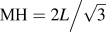 ${\rm{MH}} = {{2L} \mathord{\left/ {\vphantom {{2L} {\sqrt 3 }}} \right. \kern-\nulldelimiterspace} {\sqrt 3 }}$ into Eq. (11) now gives:
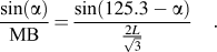 $${{\sin \left( \alpha \right)} \over {{\rm{MB}}}} = {{\sin \left( {125.3 - \alpha } \right)} \over {{\textstyle{{2L} \over {\sqrt 3 }}}}}\quad .$$
Hence, rearranging Eq. (12) now gives:
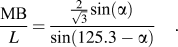 $${{{\rm{MB}}} \over L} = {{{\textstyle{2 \over {\sqrt 3 }}}\sin \left( \alpha \right)} \over {\sin \left( {125.3 - \alpha } \right)}}\quad .$$
Thus, the relationship between the angle of incidence, θ, and the angle, α, opposite to the line length MB, can be obtained by applying the sine rule to triangle MHB. Since the incidence light ray is reflected across the normal to the line MB, we can also equate the included angle to 90°. That gives:
 $$\gamma + \theta + 35.3^\circ = 90^\circ \quad .$$
Rearranging Eq. (14) now gives
 $$\gamma = 54.7^\circ - \theta \quad .$$
Also, from triangle MCB, we can deduce that:
 $$2\gamma + \theta = 90^\circ - \alpha \quad .$$
Hence, 2(54.7° − θ) + θ = 90° − α, and α is now given by
 $$\alpha = \theta ^\circ - 19.4^\circ \quad .$$
Hence, substituting Eq. (16) into Eq. (13) now gives:
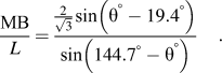 $${{{\rm{MB}}} \over L} = {{{\textstyle{2 \over {\sqrt 3 }}}\sin \left( {\theta ^\circ - 19.4^\circ } \right)} \over {\sin \left( {144.7^\circ - \theta ^\circ } \right)}}\quad .$$
Thus, the contributing factor, F X2, of the secondary reflections for this range is given by:
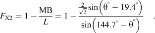 $${F_{{\rm{X}}2}} = 1 - {{{\rm{MB}}} \over L} = 1 - {{{\textstyle{2 \over {\sqrt 3 }}}\sin \left( {\theta ^\circ - 19.4^\circ } \right)} \over {\sin \left( {144.7^\circ - \theta ^\circ } \right)}}\quad .$$
For angles of incidence between 35.3° and 54.7° (Fig. 6), the part of facet X between points O and A (line length OA) does not have access to light rays due to the effects of shading. The proportion of facet X that is not accessible to light rays can thus be expressed as the ratio of the OA to the side length of the pyramid, OM or L.
Light interaction with the pyramid facet at an angle between 35.3° and 54.7°.

Hence, by applying the sine rule to triangle HOA, we obtain:
 $${{\sin \left( \beta \right)} \over {{\rm{OA}}}} = {{\sin \left( {109.4 - \beta } \right)} \over L}\quad .$$
Rearranging Eq. (19) now gives:
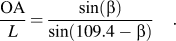 $${{{\rm{OA}}} \over L} = {{\sin \left( \beta \right)} \over {\sin \left( {109.4 - \beta } \right)}}\quad .$$
Furthermore, by substituting the angle, β, with the expression β = θ − 35.3°, we have:
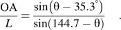 $${{{\rm{OA}}} \over L} = {{\sin \left( {\theta - 35.3^\circ } \right)} \over {\sin \left( {144.7 - \theta } \right)}}\quad .$$
Thus, the contributing factor, F X2, of the secondary reflections for this range is given by:
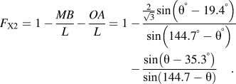 $${F_{{\rm{X2}}}} = 1 - {{MB} \over L} - {{OA} \over L} = 1 - {{{\textstyle{2 \over {\sqrt 3 }}}\sin \left( {\theta ^\circ - 19.4^\circ } \right)} \over {\sin \left( {144.7^\circ - \theta ^\circ } \right)}} - {{\sin \left( {\theta - 35.3^\circ } \right)} \over {\sin \left( {144.7 - \theta } \right)}}\quad .$$
So for all angles, F X2 can be obtained via any of the following expressions, depending on the range of the angle of incidence of the light rays:
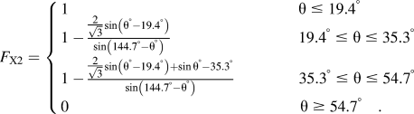 $${F_{{\rm{X}}2}} = \left\{ \matrix{ 1\quad \quad \quad \quad \quad \quad \quad \quad \quad \quad \;\;\quad \quad \quad \quad \theta \;\le\; 19.4^\circ \hfill \cr 1 - {{{\textstyle{2 \over {\sqrt 3 }}}\sin \left( {\theta ^\circ - 19.4^\circ } \right)} \over {\sin \left( {144.7^\circ - \theta ^\circ } \right)}}\quad \quad \quad \quad \quad \quad \quad \quad 19.4^\circ \;\le\; \theta \;\le\; 35.3^\circ \hfill \cr 1 - {{{\textstyle{2 \over {\sqrt 3 }}}\sin \left( {\theta ^\circ - 19.4^\circ } \right) + \sin \theta ^\circ - 35.3^\circ } \over {\sin \left( {144.7^\circ - \theta ^\circ } \right)}}\quad\quad\quad \quad 35.3^\circ \;\le\; \theta\; \le\; 54.7^\circ \hfill \cr 0\quad \quad \quad \quad \quad \!\!\quad \quad \quad \quad \quad \quad \quad \quad \quad \quad \theta \;\ge\; 54.7^\circ \quad . \hfill \cr} \right.$$
By combining the primary and secondary reflections with their contributing factors, the total reflectance can be obtained from the following expressionReference Wu, Wei and Lin26,Reference Singh, Kumar, Lal, Singh and Das27 :
 $${R_{\rm{T}}} = {R_{{\rm{X}}1}}{F_{{\rm{X}}1}}\left[ {{R_{{\rm{X}}2}}{F_{{\rm{X}}2}} + \left( {1 - {F_{{\rm{X}}2}}} \right)} \right] + {R_{{\rm{Y}}1}}{F_{{\rm{Y}}1}}{R_{{\rm{Y}}2}}\quad ,$$
where R X1 and R Y1 are the primary reflection coefficients from facets X and Y, with contribution factors of F X1 and F Y1, respectively. R Y2 is the secondary reflection coefficient from facet Y. The secondary reflection coefficient from facet X is represented by R X2 with its contribution factor being F X2. However, (1 − F X2) accounts for the light not subjected to a secondary reflection from facet X. The reflectance, R, for both the primary and secondary reflections can be obtained using the Fresnel equations adopted from Ref. Reference Pedrotti, Pedrotti and Pedrotti28. These give:
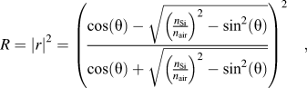 $$R = {\left| r \right|^2} = {\left( {{{\cos \left( \theta \right) - \sqrt {{{\left( {{{{n_{{\rm{Si}}}}} \over {{n_{{\rm{air}}}}}}} \right)}^2} - {{\sin }^2}\left( \theta \right)} } \over {\cos \left( \theta \right) + \sqrt {{{\left( {{{{n_{{\rm{Si}}}}} \over {{n_{{\rm{air}}}}}}} \right)}^2} - {{\sin }^2}\left( \theta \right)} }}} \right)^2}\quad ,$$
where r represents the reflection coefficient for both the primary and secondary reflections.
III. EXPERIMENTAL PROCEDURES
In an effort to validate the pyramidal structures used in the above model, the (100)-oriented silicon wafers were procured from Semiconductor Wafer Inc., Hsinchu, Taiwan. Prior to alkaline etching, the wafers were dipped in 0.5% HF for 100 s to remove native oxides and subsequently dried in nitrogen gas. Samples were etched in an alkaline solution of KOH under the etching conditions of an etch duration of 40 min, an etch temperature of 80 °C, and a volume concentration of KOH:IPA in the ratio 2:4. Also, at the end of each texturing process, the samples were rinsed in distilled de-ionized water and dried in nitrogen gas.
The alkaline etching was carried out in a GFL-1083 thermo-coupled water bath (Gesellschaft für Labortechnik (GFL), Burgwedel, Hanover, Germany). Scanning electron images of the etched and unetched silicon surfaces were then obtained using an EVO MA-10 scanning electron microscope (SEM) that was operated at 10 kV (EVO MA-10, Carl Zeiss, Hamburg, Germany).
IV. RESULTS AND DISCUSSION
A. Reflection from etched 100 silicon surfaces
A secondary electron image of an etched (100)-oriented silicon wafer surface is presented in Fig. 1. This shows clearly that pyramidal facets are formed on the silicon wafer, after etching. This has geometrical characteristics that are similar to those discussed and idealized earlier in Sec. 2. However, unlike the idealized unit cell structures, in which the pyramidal dimensions were uniform, the actual pyramidal structures exhibited variations in the unit cell heights, although the basic shapes were geometrically similar. The interactions with the incident light rays should, therefore, apply to primary reflections, since the secondary reflections may be affected by differences in the adjacent facets.
As discussed in the preceding section, the possibility that the incident light will experience a secondary reflection (double-bounce incidence) or a multiple reflection depends upon the height of the pyramid, the apex angle of the pyramid, and the facet tilt angles of the geometrical textures, with respect to the surface of the wafer.Reference Hamel and Chibani29,Reference Xi, Yang, Dan, Jun, Li and Que30 From prior work by Sethi et al.,Reference Sethi, Anand, Walia and Sood31 a secondary reflection is experienced or guaranteed, if the facet tilt angle falls within the range between 45° and 60°. Since texturing of (100)-oriented silicon wafers in the alkaline solution produces pyramids with an apex angle of 70.6° and a facet tilt angle of 54.7° for an ideal process or <52° for a non-ideal process,Reference Baker‐Finch and McIntosh16,Reference Baker-Finch22 which are within the range specified by Sethi et al.,Reference Sethi, Anand, Walia and Sood31 our model can be used to investigate the possibility of secondary reflection, for the full range of incidence angles to the substrate.
By inspection, when the angle of incidence to the substrate is less than 19.4°, secondary reflection occurs on the neighboring Y facet, for all light rays that strike any arbitrary point on X facet. This validates prior work on the reflection of normally incident light rays using the OPAL 2 softwareReference McIntosh and Baker‐Finch32,Reference Baker‐Finch and McIntosh33 to show that 88.9% of incident rays experience a double and 11.1% experience triple bounce. However, if the angle of incidence is between 19.4° and 35.3°, some light is reflected from facet X. The reflected light is directed away from the substrate, leaving only some proportion of the facet to experience secondary reflection.
In the case of incident angles between 35.3° and 54.7°, the incident light rays are not able to strike some portion of facet X. This is due to shading from facet Y. However, for incident angles equal to 54.7°, the possibility of secondary reflections is eliminated because the incident light is perpendicular to facet X. Thus, at any angle greater than 54.7°, secondary reflections cannot occur. Hence, any incident light rays that strike the textured surfaces of etched (001)-oriented silicon surfaces at low incidence angles produce more secondary reflections and thus have at least two chances of being absorbed. However, the chances of absorption are reduced at high incidence angles, where most of the reflected light rays are directed away from the substrate.
B. Total reflectances
It is important to note here that the above model does not account for the tertiary reflections, as with prior work on the reflection of normally incident sunlight.Reference Baker‐Finch and McIntosh16,Reference Baker‐Finch and McIntosh17,Reference Baker-Finch22 These were not explored, since they do not occur often for non-normal incident angles.Reference Sethi, Anand, Walia and Sood31 Furthermore, they have only a minor effect on the overall accuracy of the total reflectance.Reference Sethi, Anand, Walia and Sood31 Also, in the 2D textured surface model, the pyramids were assumed to be aligned with one another, as shown in Fig. 4. However, this is valid only for regular inverted pyramidal textures and not for randomly textured silicon wafers. Hence, a more realistic approach is needed to model the light/pyramid interactions in actual etched (001)-oriented silicon wafers with textures similar to those presented in Fig. 1. Nevertheless, the results obtained from the current idealized 2D textured surface model are close to the measured reflectance values presented by Parretta et al.Reference Parretta, Sarno, Tortora, Yakubu, Maddalena, Zhao and Wang20
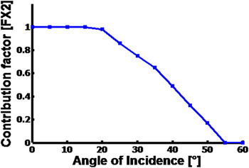
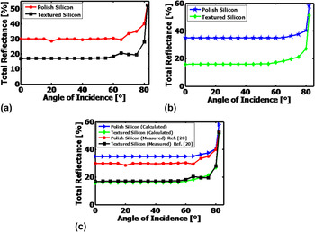
A summary of the contribution factors (F X2) obtained for different angles of incidence is presented in Fig. 7. This shows that, above the incident angle of 19.4°, F X2 decreases gradually with increasing angle of incidence. Furthermore, the dependence of the total reflectance on the angle of incidence is presented in Figs. 8(a) and 8(b), for etched (001)-oriented surfaces subjected to incident light rays with a wave length, λ, of 635 nm. In all cases, the total reflectances of the textured surfaces are lower than those of the flat polished surfaces.
The dependence of F X2 on the incidence angle.

(a) Measured total reflectance versus angle of incidence treated at λ = 633.20 (b) Calculated total reflectance versus angle of incidence treated at λ = 635. (c)The calculated and measured reflectance versus angle of incidence.

The predicted reflectances [obtained from Eq. (23)] are also in good agreement with the measured reflectance values [Fig. 8(c)]. The close agreement between the experimental and predicted reflectances suggests that the idealized model presented here captures most of the important aspects of light interactions with the pyramidal structures that are formed by the alkaline etching of (001)-oriented silicon surfaces with etchants such as KOH.
C. Implications
The implications of the above model are quite significant. First, they show that more secondary reflections are experienced on textured silicon (100)-oriented wafers at low incidence angles. The optical path lengths also increase with increasing secondary reflections, thus, providing increased chances of light absorption. This suggests that KOH textured pyramidal structures can be tailored to control their reflectance, when the angle of incidence of light and the uniformity of the pyramids are well controlled.
Furthermore, the good agreement between the measured and the predicted reflectances suggests that our 2D model captures most of the important aspects of light interactions with the pyramidal structures that are formed by the KOH-etching of (001)-oriented silicon surfaces.
These resulting reductions in surface reflectance enable more light to be trapped for conversion to charge in single crystal silicon solar cells. The control of alkaline etching can, therefore, be used to engineer the improvement of silicon solar cell efficiency. Further work is clearly needed to explore the possible improvements in solar cell efficiency that can be achieved via the controlled alkaline etching of silicon wafers in silicon solar cells.
V. CONCLUSIONS
(1) A simple analytical model has been developed and used to study the optical behavior of flat and textured silicon substrates. The model explored the possibility of secondary reflections, for the full range of incidence angles to the silicon substrate. The geometrical interactions of light rays with pyramidal facets were used to predict the reflectance values, which were compared with measurements of reflectance on alkaline textured silicon surfaces.
(2) Secondary reflection is experienced or guaranteed, for all pyramid heights, when the angle of incidence to the substrate is less than 19.4°. Hence, any incident light beams that strike the textured surfaces of etched (001)-oriented silicon surfaces at low incidence angles produce more secondary reflections than flat silicon substrates. Thus, secondary reflections increase the time available for the incident light rays to be absorbed into (001)-oriented silicon single crystals.
(3) The predictions obtained from the current 2D textured surface model are close to the measured reflectance values presented in Ref. Reference Parretta, Sarno, Tortora, Yakubu, Maddalena, Zhao and Wang20. The close agreement between the experimental and predicted reflectances suggests that the idealized model presented here captures most of the important aspects of light interactions with the pyramidal structures that are formed by the alkaline etching of (001)-oriented silicon surfaces with etchants such as KOH.
(4) The current results suggest that the model can be helpful in the design of textured silicon surfaces for the control of surface reflectance and the trapping of light by secondary reflections. Such control and trapping could lead to increased photoconversion and silicon solar cell efficiency.
ACKNOWLEDGMENTS
The authors are grateful to thank Prof. Oleg Yordanov, Bruno Dandogbessi, and Uche Opara for useful scientific discussions. Appreciation is also extended to the World Bank STEP-B Program, the World Bank African Centers of Excellence Program, the African Development Bank, the African Capacity Building Foundation (ACBF), and the Nelson Mandela Institute for financial support.