I. INTRODUCTION
Since the discovery of colossal magnetoresistance and high-temperature superconductivity in perovskite transition metal oxides, much effort has been devoted to understanding of the unusually electronic and magnetic properties of these materials. Especially, the layer-type perovskite oxides of Ln2–xAxBO4 (Ln: lanthanides; A: alkaline earth elements, B: transition metal elements) with a K2NiF4-type structure have aroused much attention for their structural similarity with high-temperature superconductors as well as their anisotropic magnetotransport properties.Reference Chichev, Dlouha, Vratislav, Knizek, Hejtmanek, Marysko, Veverka, Jirak, Golosova, Kozlenko and Savenko1–Reference Wu and Neumeier3 The presence of rocksalt layer Ln/A–O induces the characteristic of a two-dimensional (2D) confinement, which significantly reduces the bandwidth of the eg electrons in the system and therefore influences the freedom of charge, spin, and orbit.
Recently, the layered perovskite cobaltite, Nd2–xSrxCoO4 in the doping range of 1.25 ≤ x ≤ 1.60 has been investigated systematically in our group.Reference Huang, Ruan, Lv, Zhuang, Wei, Wu, Li, Zhang, Chai, Yang, Cao and Li4, Reference Huang, Ruan, Lv, Wu, Pang, Cao and Li5 We found that as temperature lowered, the polycrystalline specimens underwent a transformation from paramagnetic phase, through Griffiths phase and ferromagnetic phase, to spin-glass reentry. We also examined the transport properties of the specimens but drew some controversial conclusions.Reference Huang, Ruan, Lv, Zhuang, Wei, Wu, Li, Zhang, Chai, Yang, Cao and Li4, Reference Matsuno, Okimoto, Fang, Yu, Matsui, Nagaosa, Kawasaki and Tokura6, Reference Wang and Takayama-Muromachi7 The resistivity (in the doping range of 1 ≤ x ≤ 2) and thermopower (in the doping range of 1.25 ≤ x ≤ 1.60) of the polycrystalline specimens below room temperature indicated a semiconducting property. No anomaly was found at the magnetic-transitional temperatures. However, for Sr2CoO4 thin film,Reference Matsuno, Okimoto, Fang, Yu, Matsui, Nagaosa, Kawasaki and Tokura6 a clear anisotropy was observed in the resistivity and a metal-insulator transition presented at Curie temperature T C.
It is well known that the transport properties of the transition metal oxides are largely determined by the hybridization of transition metal (3d orbital) with oxygen (2p orbital). The spin fluctuations should contribute to the transport phenomena because they scatter conduction electrons through the exchange interaction.Reference Gratz8 To obtain more information about the conduction mechanisms of the layered cobaltite, temperature dependence of the resistivity and the thermopower was investigated for the Nd0.75Sr1.25CoO4 (NSCO) thin film in the a-b plane. The thermopower of the specimen could be well accounted for by the spin-dependent scattering of the charge carriers, whereas the conduction of the specimen could be well interpreted by the small polaron hopping conduction in the nonadiabatic regime at high temperatures combined with a 2D variable range hopping of small polarons at low temperatures.
II. EXPERIMENTAL
By employing a pulsed laser deposition method with a KrF excimer laser (λ = 248 nm), thin film of NSCO was grown on (100)-LaAlO3 (LAO) and (100)-LaSrAlO4 (LSAO) substrates with a typical dimension of 5 × 5 × 0.5 mm3. A target with the nominal composition was prepared by a nitrate decomposition methodReference Sanchez-Andujar and Senaris-Rodriguez9 where the annealing temperature was set at 1250 °C instead of 975 °C. The film was then epitaxially grown at 710 °C under 40 mTorr oxygen pressure.
The crystal structures of the target and the film were characterized by x-ray diffraction (XRD) measurement with Cu Kα radiation. The thickness and surface morphology of the film were measured by a JSM-6700F scanning electron microscope (SEM; JEOL, Tokyo, Japan). The compositional analysis of the film was carried out using an energy dispersive x-ray (EDX) spectroscopy as attached on the SEM. All measurements were taken at room temperature in normal conditions.
The resistivity (ρ) measurements were carried out in the a-b plane of the film by a home-built four-probe device equipped with a Lakeshore temperature controller (Model No. 340, Lake Shore Cryotronics, Westerville, OH). For the measurements the film with the substrates was cut into pieces in the dimension of 5 × 2 × 0.5 mm3. Four gold spots were then deposited on the surface of the film in an identical distance (~1.4 mm) before copper wires were attached with silver epoxy. The specimen temperature was kept constant within ±1 K during the measurements.
The thermopower (S) was defined as the thermoelectric voltage per degree of temperature difference (ΔV/ΔT) and the measurements were performed in the a-b plane of the film by a homemade apparatus, in which the steady-state technique of alternating the temperature gradient was used as described in Ref. 10. The films were placed between two copper electrodes, and an appropriate temperature gradient of 2 K was maintained between them. After measurements the absolute thermopower values of the specimens were obtained by subtracting the contribution of the copper leads. The error of the measurement system was <0.1 μV/K. The data were collected with decreasing temperature in a temperature range of 300–76 K for ρ and a temperature range of 310–80 K for S where the large resistance of the NSCO thin film at lower temperatures exceeded the upper measurement limit of our setup.
With a physical property measurement system (PPMS; Quantum Design, San Diego, CA), direct current (dc) magnetization was measured within a temperature range from 5 to 300 K under an applied magnetic field of 1000 Oe in the field-cooling (FC) model.
The results were reproducible on other specimens, such as NSCO thin film on (001)-LSAO, (100)-MgO, and (100)-SrTiO3 substrates. The thickness of the films varied from 50 to 120 nm. The resistance was so large that the thermoelectric measurements could only be performed in a limited high-temperature range. Therefore, in the article we only explained the results of the film on (100)-LAO and (100)-LSAO substrates.
III. RESULTS
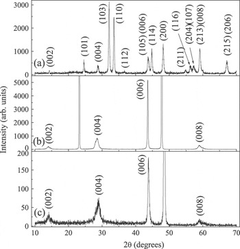
Figure 1 shows the XRD profiles of NSCO target and NSCO thin film. For the target, the diffraction peaks are well indexed with K2NiF4-type tetragonal structure described by the I4/mmm space group, but for the thin film only diffraction peaks along the c direction are observed in the patterns, indicative of a single phase of the film with K2NiF4 structure that epitaxially grew along the c axis. As revealed in the XRD profiles, the crystalline quality of the film on LAO seems better than that on LSAO.
XRD profiles for (a) NSCO ceramic, (b) NSCO thin film on LAO substrate, and (c) NSCO thin film on LSAO substrate at room temperature.

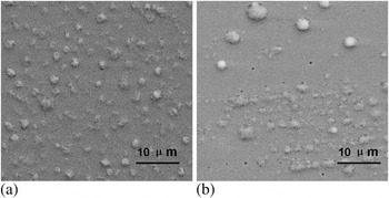
Figure 2 presents the SEM images of NSCO thin film grown on different substrates. There are a few spherical droplets formed on the smooth surface of the deposited film. Elemental analysis of EDX spectra suggests that the droplets and the film are of uniform chemical contents with fairly similar stochiometric ratio. The diameter of the droplets is ~1.5 μm on the LAO substrate while it ranges from 0.6 to 5.0 μm on the LSAO substrate. Moreover some nano-sized pores appear in the film on the LSAO substrate, indicating a relatively poor surface morphology. The thickness of the films, as observed by the cross-sectional SEM images, is 240 nm on LAO substrate and 490 nm on LSAO substrate.
Surface images of the NSCO thin film on (a) LAO substrate and (b) LSAO substrate.

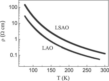
Figure 3 shows the measured dependence of the ab-plane resistivity ρ on the temperature of NSCO thin film grown on different substrates. In contrast to the metallic nature of the parent compound Sr2CoO4 thin film in the a-b plane,Reference Matsuno, Okimoto, Fang, Yu, Matsui, Nagaosa, Kawasaki and Tokura6 the resistivity herein presents a semiconducting nature of temperature dependence without any distinct anomaly or jump over the whole temperature range.
Temperature dependence of the ab-plane resistivity ρ for NSCO thin film grown on LAO and LSAO substrates.

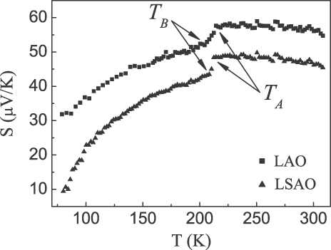
Figure 4 presents the measured temperature dependence of the ab-plane thermopower S of NSCO thin film grown on different substrates. Within the measured temperature range, a positive Seebeck coefficient S(T) is observed. In detail, with decreasing temperature the Seebeck coefficient is almost independent of temperature when T > T A, nevertheless, it presents a steplike decrease in a limited temperature range of T B < T < T A and a further continuous decrease when T < T B. The critical temperature points of T A and T B are respectively 214.4 and 204.4 K for the film on LAO and 212.4 K and 208.4 K for the film on LSAO. The positive S(T) indicates that the majority of charge carriers are holes. Except for the steplike decrease between T A and T B, the temperature evolution of the thermopower for the thin film is analogous to that of La2–xSrxCoO4 compound with uniform structure.Reference Chichev, Dlouha, Vratislav, Knizek, Hejtmanek, Marysko, Veverka, Jirak, Golosova, Kozlenko and Savenko1 The result suggests that they may arise from the same mechanism where the low-temperature downturn of the thermopower evidences the presence of a finite density of states at the Fermi level.
Temperature dependence of the ab-plane thermopower S for NSCO thin film grown on LAO and LSAO substrates.

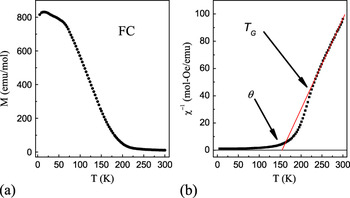
We had attempted to achieve dc magnetization of the thin film, but the demagnetizing effect of the substrates was so large that the magnetic properties of the film could not be obtained via our measurement system. Finally, we performed only magnetization experiment on the target pellet instead of thin film. Figure 5 shows the relations of FC magnetization and inverse susceptibility with temperature for the NSCO ceramic. The magnetization value and its temperature evolution in Fig. 5 are analogous to those of polycrystals annealed at 975 °C,Reference Huang, Ruan, Lv, Zhuang, Wei, Wu, Li, Zhang, Chai, Yang, Cao and Li4 indicating that the annealing at 1250 °C has little influence on the magnetic properties for the sample. As confirmed by the measurementsReference Huang, Ruan, Lv, Zhuang, Wei, Wu, Li, Zhang, Chai, Yang, Cao and Li4, Reference Huang, Ruan, Lv, Wu, Pang, Cao and Li5 of magnetic hysteresis, alternating current (ac) susceptibility and electron-spin resonance, the specimen undergoes a transformation from paramagnetic phase, through Griffiths phase and ferromagnetic phase, into spin-glass reentrance. The Griffiths temperature T G and Weiss temperature θ, as characterized by the arrows in Fig. 5(b), are 225.2 and 156.7 K, respectively, for the specimen.
Temperature dependence of (a) the FC magnetization and (b) the inverse susceptibility for NSCO ceramic. The solid line is the best fit to the Cure–Weiss law in the paramagnetic range, T > T G.

IV. DISCUSSION
The aforementioned measured results reveal that the resistivity magnitude of the film on LAO substrate is smaller than that on LSAO substrate but the thermopower magnitude of the film on LAO substrate is larger than that on LSAO substrate, although both have similar temperature dependence. Because the mismatch between the film and the substrates would introduce strain to the film, the influence of the strain on the specimens may induce the previously observed magnitude differences of the resistivity and the thermopower. In contrast to that of the ceramic,Reference Huang, Ruan, Lv, Zhuang, Wei, Wu, Li, Zhang, Chai, Yang, Cao and Li4 the ρ value of the film herein becomes much smaller, although the S is much larger than that of the ceramic.Reference Huang, Ruan, Lv, Zhuang, Wei, Wu, Li, Zhang, Chai, Yang, Cao and Li4 The phenomenon is consistent with the quasi-2D electronic nature of the specimen. In the Sr2CoO4 film,Reference Matsuno, Okimoto, Fang, Yu, Matsui, Nagaosa, Kawasaki and Tokura6 the out-of-plane resistivity ρc is much higher than the in-plane resistivity ρab. The ratio of them, ρc/ρab, ranges from 120 to 150 over the whole temperature region that was investigated. In our experiment, the S and ρ were measured only in the weak-semiconducting a-b plane. The improved carrier mobility thus decreases the ρ and consequently increases the S for the transition metal oxides with intense phonon drag.
It is worth noting that the limited temperature region for the steplike decrease in S is just close to the Griffiths temperature, T G and the continuous decrease in S is in the Griffiths and ferromagnetic states. Similar to the case in La2–2xSr1+2xMn2O7,Reference Nakamae, Colson, Forget, Legros, Marucco, Ayache and Ocio11 this coincidence should be due to the spin alignment that reduces the spin dependent scattering of the charge carriers and thus decreases the diffusive term in the Seebeck coefficient. It is believed that the steplike decrease of S comes from the abrupt spin alignment from the paramagnetic phase to Griffiths phase. For the continuous alignment of the spins in the Griffiths and ferromagnetic phases, the S value decreases successively and does not present any anomaly.
In analogy to previous studies on transition metal oxides, we have performed an analysis on the specimens in terms of small polaron hopping conduction where the conductivity can be expressed by the general formulaReference Mott12, Reference Austin and Mott13:

where W is the activation energy, σ0 is the pre-exponential factor given as

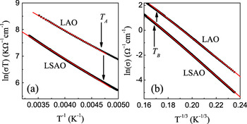
where k B is the Boltzmann constant, v ph is the optical phonon frequency, N is the concentration of the transition metal ions, R is the average spacing between the transition metal ions given as R = N −1/3, C is the fraction of the transition metal ion concentration in the low valence state to the total transition metal ion concentration, and α−1 is the localization length. The exponential factor exp(−2αR) reduces to 1 in the adiabatic case, otherwise it is nonadiabatic.Reference Mott12 We found that the electrical conductivity of the film cannot be fitted with the small polaron hopping model in the whole temperature range studied, only the data above T A can be well applied. Figure 6(a) shows the plots of ln(σT) versus T −1 for NSCO thin film on LSAO and LAO substrates. The linear fit yields the values of W in Table I, which are compatible with those reported for other transition metal oxides.Reference Banerjee, Pal, Rozenberg and Chaudhuri14–Reference Lago, Battle, Rosseinsky, Coldea and Singleton16 For the thin film, the value of v ph can be estimated from the relationReference Nagaraja, Sankarappa and Prashant Kumar17:

The plots of (a) ln(σT) versus T− 1 and (b) ln(σ) versus T −1/3 for NSCO thin film grown on LAO and LSAO substrates. The solid lines in (a) and (b) respectively correspond to the least-square fitting with small polaron hopping and variable range hopping conduction models.

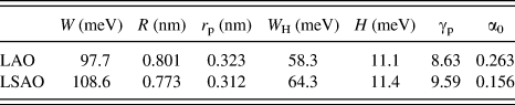
Deduced values of the activation energy W, the average spacing between the transition metal ions R, the polaronic radius r p, the polaronic hopping energy W H, the critical bandwidth H, the polaronic coupling constant γp, and the proportionality constant between the heat transfer and kinetic energy of an electron α0 for the NSCO thin film on LAO and LSAO substrates.

where θ is the Weiss temperature. With a value of 156.7 K for θ as obtained from the magnetization measurement, we can get v ph = 3.27 × 10¹² Hz. Given that the composition of the film is consistent with the nominal stoichiometry, the value of C can be derived to be 0.75 with the relation:

In this case, the polaronic density at Fermi level N(E F) is estimated to be 4.76 × 10²¹ eV−1cm−3 by using the unit cell volume of 157.5 Å3 derived from XRD data. With the values of N(E F) and W, the value of R is calculated using the relationReference Mott and Davis18:

As a scale of the polaronic dimension, the polaronic radius can be derived from the formulaReference Yildiz, Lisesivdin, Kasap and Mardare19:

And the polaronic hopping energy can be expressed asReference Yildiz, Lisesivdin, Kasap and Mardare19

With the values of W H and v ph, the polaronic coupling constant can be obtained with the relationReference Mott12:

The derived values of the aforementioned parameters are listed in Table I for the thin film on different substrates. The value of r p is found to be about 0.3 Å, which is much smaller than that of R. This obviously suggests that the polarons are indeed small polarons and they are localized in the cobalt sites. The value of γp is estimated to be about 9 for both specimens. As a measure of the electron-phonon interaction, a value of γp larger than 4 generally indicates strong electron-phonon interaction in solids.Reference Mott and Davis18 Therefore, the electron-phonon interaction in the thin film is confirmed to be very strong.
For the electrical conductivity of the thin film associated with the small polaron hopping, it is important to distinguish between the adiabatic case and the nonadiabatic case. According to Holstein’s relation,Reference Holstein20, Reference Emin and Holstein21 the polaronic bandwidth, J, should observe the conditions:
J > H for adiabatic hopping conduction and,
J < H for non-adiabatic hopping conduction,
where

The value of J can be estimated from the approximate relation at high temperatures,Reference Mollah, Khan, Shukla, Arshad, Kumar and Das15

By using the previously obtained values of W H, v ph, and θ, and selecting a representative temperature point where the Seebeck coefficient remains constant, such as T = 256 K, the values of J and H are calculated. The calculated value of J is 10.24 meV and the calculated values of H are listed in Table I. It is obvious that the J is smaller than H, suggesting a nonadiabatic hopping conduction for the thin film. Moreover, the condition for small polaron formation is J < W H/3, otherwise there will be large polarons.Reference Holstein20 In Table I the value of W H/3 is around 20 meV, much larger than J. Therefore, the conduction of the thin film in the a-b plane is via small polaron hopping conduction in the nonadiabatic regime.
In fact, the small polaron hopping conduction can also sustain with the plateau of Seebeck coefficient above T A in Fig. 4. In the case of the polaronic conduction, for a fixed concentration of charge carriers, the S(T) approaches saturation when the thermal energy becomes larger than the polaronic bandwidth. In this case, the S(T) would observe Heikes formulaReference Heikes22 as expressed by

where α0 is a constant of proportionality between the heat transfer and kinetic energy of an electron. If α0 < 1, small polaronic conduction would occur and if α0 > 2 large polarons would be involved.Reference Pal, Hirota, Tsujigami and Sakata23 The β is a spin-degeneracy factor and takes a value of either 1 or 2. Hops in the nonspin degeneracy when β = 1 is expected in a ferromagnetic regime. However, twofold spin degeneracy when β = 2 is predicted in a paramagnetic regime. As confirmed in Fig. 5, the sample exhibits a paramagnetic state above T A, which suggests that β = 2 for S in the plateau range. Via Eq. (11), α0 is calculated with a mean value of S in the plateau and a value of C at 0.75. The calculated results are listed in Table I. The values of α0 are both far less than one, suggesting that the conduction of the film is indeed with the small polaron hopping.
According to the hopping theory, the conduction mechanism in the solid generally changes from the thermally activated small polaron hopping to the variable range hopping conduction with decreasing temperature.Reference Friedman and Holstein24 As shown in Fig. 6(b), the conductivity of the thin film below T B can be well fitted with the Mott’s variable range hopping in the 2D model,Reference Mott and Davis18

where σ0 is the pre-exponential factor and T 0 is a constant depending on the density of states at the Fermi level N(E F) and is given as

The linear fit in Fig. 6(b) yields the value of T 0 = 4.58 × 10⁵ K for the thin film on LAO and 5.92 × 10⁵ K for the thin film on LSAO. The obtained value is one order of magnitude lower than those of perovskite manganates,Reference Lago, Battle, Rosseinsky, Coldea and Singleton16 which is consistent with the high value of N(E F) for the polaronic hopping conduction.Reference Banerjee, Pal, Rozenberg and Chaudhuri14
Hence, the transport properties in the a-b plane of the thin film evolve from nonadiabatic small polaron hopping conduction to variable range hopping conduction with decreasing temperature. The polaronic conduction may stem from several factors for the thin film. First, similar to the Jahn–Teller distortion of the MnO3 tetragonal structure in the manganates,Reference Millis25 the Jahn–Teller distortion of the CoO3 tetragonal structure may also exist in the cobaltite thin film. Thus, the Jahn–Teller phonon models would split the twofold eg orbital degeneracy and induce a narrow conduction band for the system. Second, the 2D structure of the specimen herein presents a quasi-2D electronic nature, which would lead to the anisotropic reduction of the bandwidth. In addition, the local disorder for the substitutional defects might also play an important role. All these would result in a strong electron-phonon coupling for the thin film as observed. At high temperatures the charge carriers are dressed by the surrounding ions but become quite mobile. At low temperatures the cobalt ions are frozen into their discrete positions, which would act like the domain wall for the system. The charge carriers would prefer to hop among the nearest neighbors. In such a case, the variable range hopping of small polarons would dominate the conduction.
V. CONCLUSION
In summary, the resistivity (in the temperature range of 76–300 K) and the thermopower (in the temperature range of 80–310 K) of the NSCO thin film in the a-b plane were respectively investigated. The specimen exhibited p-type semiconducting transport properties. The thermopower presented a plateau at high temperatures and decreased at low ones with an additional steplike decrease in a limited temperature range. In contrast to the magnetic properties of the specimen, the decreasing thermopower was chiefly ascribed to the spin alignment that reduced the spin-dependent scattering of the charge carriers, and the steplike decrease was attributed to the abrupt spin alignment from paramagnetic phase to Griffiths phase. The conduction at high temperatures could be well interpreted in terms of small polaron hopping conduction in the nonadiabatic regime, but it changed to variable range hopping of small polarons with decreasing temperature. In addition to the Jahn–Teller distortion of the CoO3 tetragonal structure, the polaronic conduction might be also due to the anisotropic reduction of the bandwidth for the 2D structure of the specimen and the local disorder for the substitutional defects. All these resulted in a strong electron-phonon coupling for the system.
ACKNOWLEDGMENTS
This work was supported by the China–MOST International Sci & Tech Cooperation and Exchange Project under Grant No. 2008DFA51230; National Key Basic Science Research Program (973 Project) under Grant No. 2007CB936603; NSFC projects under Grant Nos. 11074207, 60776007; and the Faculty Start-up Fund at Xiamen University under Grant No. X12111.