


Introduction
Shaping an electron beam for clinical use can be challenging due to the high susceptibility of electrons to in-air scattering events. The most common approach for electron beam shaping is similar to the one proposed by Goede et al. in 1977 Reference Goede, Gooden, Ellis and Brickner1 and involves the use of an electron cutout block secured in close proximity to the patient’s skin. Reference Hogstrom and Almond2 The block is composed of a low melting point alloy (LMPA) and contains an aperture which is scaled to provide the desired field size and shape at the prescription source-to-surface distance. Although recent works have investigated the use of alternative collimation options for electron beams – such as tungsten-containing rubber shielding, Reference Kijima, Monzen, Matsumoto, Tamura and Nishimura3 specialised electron multi-leaf collimators (MLC), Reference Ma, Pawlicki and Lee4,Reference Eldib, ElGohary and Fan5 and conventional photon MLC Reference Mueller, Fix and Henzen6,Reference Ma, Parsons and Chen7 − these alternatives are still being refined and have not yet been adopted in routine clinical practice.
Electron cutout blocks are commonly made using Cerrobend (also known as Wood’s metal or Lipowitz’s alloy) or a similar LMPA. A Styrofoam aperture ‘negative’ is manually aligned to the desired location in the insert frame and then molten LMPA is poured in the frame. Once the LMPA has cooled to room temperature, the Styrofoam negative is removed and the block can be used for patient treatment. While this approach is effective and widely used for producing clinically viable electron blocks, it also has inherent limitations. For example, some of the steps in the process – such as the manual positioning of the negative in the frame – are subjective and prone to user error. Reference Skinner, Fahimian and Yu8 Furthermore, at our centre, we have observed that the force of the molten LMPA against the sides of the insert frame can result in appreciable bowing, making the frames unusable clinically and sometimes necessitating several pours before an acceptable electron block is achieved.
In recent years, three-dimensional (3D) printing has found uses in several facets of radiation therapy, including brachytherapy, Reference Sekii, Tsujino and Kosaka9–Reference Cunha, Mellis and Sethi11 quality assurance Reference Tino, Yeo, Leary, Brandt and Kron12–Reference Kumar, Sharma and Despande14 and electron beam therapy. Reference Skinner, Fahimian and Yu8,Reference Michiels, Mangelschots, Roover, Devroye and Depuydt15–Reference Su, Moran and Robar18 Much work has been done to evaluate the dosimetric properties of different 3D printable filaments, as well as the spatial accuracy of the phantoms that can be produced with the technique. Reference Filippou and Tsoumpas19–Reference Kairn, Crowe, Markwell and Jaffray21 One area of interest is the applicability of 3D printing techniques for improvement of the electron block fabrication process. Michiels et al. demonstrated a workflow utilising a 3D printed positioning device and a polylactic acid (PLA) aperture negative for electron block fabrication. Reference Michiels, Mangelschots, Roover, Devroye and Depuydt15 This technique alleviated the need for the Styrofoam negative and block cutter, as well as manual negative positioning; however, each 3D printed negative required between 1 and 9 hours of printing time. Furthermore, while PLA filament is a common choice in 3D printing applications for radiation therapy, Reference Filippou and Tsoumpas19 its low glass transition temperature of approximately 60°C is problematic. The melting temperature of Cerrobend is 70°C, and so when using PLA, there is potential for the 3D printed parts to deform, compromising the final field shape. This issue is more pronounced when using cadmium-free alloys, such as those proposed by Blackwell and Amundson, Reference Blackwell and Amundson22 since the melting point of cadmium-free LMPA is 95°C. For these reasons, the use of 3D printed PLA components for electron block fabrication is sub-optimal and precludes its use as a widespread replacement for conventional electron block fabrication methods.
In this work, we propose an alternative 3D printing method for electron block production. We investigate the use of another commonly used 3D printing filament material, Acrylonitrile Butadiene Styrene (ABS), as an alternative to PLA. The glass transition temperature of ABS is 105°C, which is significantly higher than that of PLA and is appropriate for use with cadmium-free LMPA. We present a 3D printed negative design, which compared to other 3D printed approaches requires a minimal amount of filament and considerably less printing time. Furthermore, our technique enables the fabrication of complex electron blocks consisting of multiple precisely positioned apertures which can, for example, be used to passively modulate the intensity of the electron beam. Reference Hogstrom, Carver, Chambers and Erhart23 Finally, we demonstrate that the use of a 3D printed alignment jig designed to match the outer contours of Varian electron insert frames can be used to minimise frame bowing and increase the usable lifetime of insert frames in the clinic.
Materials and Methods
Insert design and printing
Patient treatment plans containing electron aperture blocks were exported from the Eclipse Treatment Planning System (TPS) version 13.6 (Varian, Palo Alto, USA) in DICOM RT file format. A customised Python script was used to automatically generate the corresponding stereolithography (STL) file for the 3D printable negative from the DICOM file. In brief, the beam block data were read from the DICOM file using the freely available pydicom module, and the coordinates of each control point in the block contour were extracted. The coordinates were scaled to represent the contour at an SSD of 95 cm. The Python FreeCAD module was used to generate a wire structure from the contour points. A second wire structure was created within the first wire by applying a 4 mm offset towards the contour interior. The area between these two wires was extruded to form a shell in the shape of the desired cutout with a height of 20 mm and a thickness of 4 mm. In-plane and cross-plane support beams are automatically added to the interior of the shell for increased stability. Finally, an alignment ‘lock’ was added to the main in-line support, facilitating proper alignment of the negative in the jig. The last step in the script generates a 3D printable STL file. A custom Python GUI was developed that allows the user to browse for and import the desired DICOM RT file and specify the save path for the STL file produced. The GUI displays a 2D Beam’s Eye View of the cutout aperture, a 3D rendering of the STL file, and treatment parameters such as patient name, MRN, applicator size and SSD.
All 3D printing was performed using a Raise3D N2 printer (Raise3D, CA, USA) with ABS as the printing material. The STL file was imported into Simplify3D for slicing and g-code generation. A print speed of 4000 mm/min, 50% infill and 0.35 mm layer height was set. The ABS was extruded from a 0.6 mm diameter nozzle at a temperature of 240°C, and the print bed was maintained at a temperature of 110°C. After printing, the top surface of the negative was briefly sanded using 150C fine grit sandpaper to minimise any small gaps between the ABS and acrylic base plate caused by surface imperfections.
Jig design and printing
A contour gauge was used to acquire the exterior profile of a Varian III electron block insert frame (Varian, Palo Alto, USA). The 2D profile was reproduced as a sketch in Autodesk Inventor (Autodesk Inc., CA, USA) and extruded. Two work planes were added to the model such that they intersected opposite corners of the extruded part at 45° angles and met at the origin of the sketch. The part was mirrored first across one plane (producing an L-shaped part) and then across the second plane, producing the completed frame. Jigs of different size can easily be generated by modifying the length of the initial extrusion. Two perpendicular support bars were added through the geometrical centre of the frame, and an alignment key was extruded at their intersection. The model’s STL was exported and sliced using Simplify3D (Simplify3D, OH, USA). The printer settings used were identical to those in the previous section, with the exception of the layer height, which was set to 0.25 mm. The print bed was coated with a thin layer of adhesive (Magigoo) to ensure that the frame adhered to the bed for the duration of the print.
Single aperture electron block preparation and evaluation
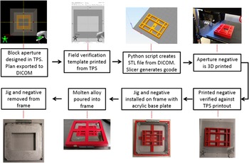
Electron blocks were prepared using the cadmium-free LMPA LOW-203 (Alchemy Extrusions Inc., On, Canada) composed of 52.5% bismuth, 32% lead and 15.5% tin. It has a melting point of 95°C, equivalent to the alloy initially proposed by Blackwell and Amundson. Reference Blackwell and Amundson22 The workflow for generating 3D printed electron cutouts is shown in Figure 1. In brief, the field verification template corresponding to the 3D printed negative was printed from the TPS and used as an initial verification of the 3D printed negative dimensions. The insert frame was then placed into the jig, ensuring that the jig notches matched the tabs on the frame exterior. Correct placement of the negative in the jig was facilitated by matching the lock-and-key pair. The acrylic base plate was inserted into the frame, and masking tape was used to secure the base to the jig to prevent unwanted leakage. The molten LMPA was added to the frame and left to cool. Upon reaching room temperature, the jig and negative were removed and any sharp edges on the interior of the aperture were filed.
An overview of the workflow for generating an electron block using the 3D printed jig and a 3D printed aperture negative designed in Eclipse.

Sheets of EBT3 gafchromic film were used to evaluate the shape of the field produced by the completed electron blocks. The film was taped to the top of a stack of 10 cm of solid water at an SSD of 100 cm and irradiated using a Varian TrueBeam accelerator. Post-irradiation, the film was digitised using an Epson Expression 10000 XL flatbed scanner, imported into DoseLab (Varian Medical Systems, CA, USA) and co-registered against the corresponding 2D dose distribution exported from the Eclipse TPS. Horizontal and vertical profiles and the corresponding full-width at half-maximum (FWHM) values were determined. A Sun Nuclear IC Profiler was also used to acquire field profiles as a secondary check.
Multi-aperture electron block preparation and evaluation
Two multi-aperture electron blocks were fabricated using the passive electron intensity modulation methodology developed by Hogstrom et al. Reference Hogstrom, Carver, Chambers and Erhart23 . In this technique, a block containing a hexagonal grid of apertures is used to spatially modulate the intensity of an electron beam. The aperture diameter, d, required to produce a beam of relative intensity, I, with respect to an open field is given by
 $$d = r * {\left( {{I \over {100}} * {{2\sqrt 3 } \over \pi }} \right)^{{1 \over 2}}}$$
where r is the inter-aperture spacing. For this work, a constant spacing of r = 15 mm was used. To ensure proper positioning of the grid, the alignment lock was generated in the centre of a rectangular base, from which the hexagonal grid of aperture negatives was extruded. The multi-aperture negatives were 3D printed, and blocks were prepared in 15×15 cm2 insert frames as described in the previous section. Profiles for an open 15×15 cm2 field as well as passively modulated fields were acquired using the Sun Nuclear IC Profiler.
Results and Discussion
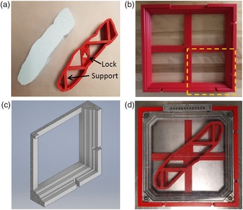
A comparison of a standard Styrofoam negative and a 3D printed negative is shown in Figure 2(a). The addition of cross-plane and in-plane supports to the interior of the 3D printed negative increases the structural integrity of the part and prevents elastic deformation when surrounded by the molten alloy. The 3D printing technique used in previous works Reference Michiels, Mangelschots, Roover, Devroye and Depuydt15 minimises elastic deformation by printing solid top and bottom layers for the negative and using several shell layers as well as 5% infill; however, this approach increases the amount of filament used for each print and would significantly increase printing time when large cutout negatives are required. The T-shaped lock is printed only on one face of the negative, ensuring that only one orientation of the negative in the jig is possible. An image of the 3D printed jig for the 20×20 cm2 insert frame is shown in Figure 2(b). The yellow dashed box indicates the region corresponding to the quarter cross-sectional view of the jig as shown in Figure 2(c). The interior contours of the jig were designed to provide surface contact to the unique contours on the exterior of the insert frame, providing increased support and decreasing the probability of frame bowing. An image of the assembled frame, 3D printed jig and 3D printed negative for a clinical plan is shown in Figure 2(d).
Examples of 3D printed components used for electron block fabrication. (a) Comparison of a traditional electron block negative generated using a Styrofoam cutter (left) and a 3D printed electron block template (right). The supports and alignment lock for the 3D printed cutout are indicated with arrows. (b) An image of the 3D printed jig used to provide support to the frame and align the printed template. (c) A quarter-cut cross section of the dashed region indicated in (b), showing the internal contours of the jig. (d) A close-up of the assembled jig, frame, cutout negative and acrylic plate.

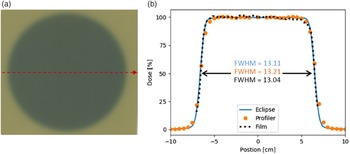
To evaluate the geometrical accuracy of the blocks produced with our 3D printed negatives, a block designed to produce a 13 cm circular field was fabricated. A photograph of EBT3 film irradiated with the block in place is shown in Figure 3(a). Line profiles through the centre of the planning system and film dose distributions are shown in Figure 3(b), along with a field profile acquired using a Sun Nuclear IC Profiler. Good agreement was observed between the appearance of the calculated and experimentally measured profiles and FWHMs, demonstrating preservation of the planned field size and a lack of deformation when using the 3D printed negatives.
Analysis of the field produced by a 6 MeV electron beam shaped using a 3D printed electron block designed to provide a 13 cm circular field at 100 cm SSD. (a) Scanned image of Gafchromic film used for measurement. The dashed line indicates the position through which a line profile was acquired. (b) A comparison of line profiles generated using the calculated Eclipse distribution as well as experimentally acquired line profiles from the film and a Sun Nuclear Profiler IC. The full-width at half-maximum (FWHM) in cm is indicated for each profile.

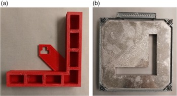
A potential disadvantage with 3D printing approaches that utilise positioning devices is that the lock must be printed within the contour of the negative itself. It is thus not possible to generate blocks containing off-axis apertures which do not intersect the geometric centre of the frame. In our technique, this is overcome by adding an additional diagonal alignment bar containing the lock to the negative, so that it may accurately align with respect to the geometrical centre of the jig. An example of an L-shaped 3D printed negative and the corresponding electron block are shown in Figure 4(a) and 4(b), respectively. While the technique of Skinner et al. Reference Skinner, Fahimian and Yu8 overcomes this limitation by extruding the aperture contour from a 3D printed tray, the amount of time and material required to print a blank tray on a per-patient basis for applicators larger than 20×20 cm2 applicator makes such an approach sub-optimal for routine use.
(a) 3D printed negative for an off-axis L-shaped field. (b) The corresponding off-axis electron block.

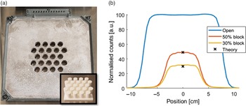
Conventional electron blocks consist of single apertures with contiguous contours; however, techniques such as spatial fractionation with electron grid therapy Reference Tamura, Monzen, Kubo, Hirata and Nishimura24,Reference Meigooni, Parker, Zheng, Kalbaugh, Regine and Mohiuddin25 and passive electron intensity modulation Reference Hogstrom, Carver, Chambers and Erhart23 require blocks containing several precisely placed beam apertures. One of the reasons that these electron grid treatments are not widely used is the difficulty associated with block creation. Reference Buckey, Stathakis and Cashon26 Using the conventional block-cutter technique would necessitate tedious manual placement of numerous Styrofoam negatives and could lead to imprecision in the final grid layout. As a proof of concept, we designed and printed two aperture negative grids for passive electron intensity modulation. Equation 1 was used to calculate the aperture diameter required to produce intensity modulations of approximately 30% (d ≈ 8.6 mm) and 50% (d ≈ 11 mm) with respect to an open field. An image of a completed multi-aperture block and the 3D printed negative used for its creation are shown in Figure 5(a). Field profiles for the multi-aperture blocks as well as an open 15×15 cm field are shown in Figure 5(b), along with the theoretical field intensity for the block predicted using Equation 1. Good agreement was observed between the measured and theoretically predicted intensity modulation, with less than a 0.3% difference for the block with 11 mm apertures and a 3.2% difference for the block with 8.6 mm apertures. Our 3D printed negatives can be precisely designed digitally and then printed as a single conjoined piece and offer increased flexibility for the placement and size of the individual apertures compared to the Styrofoam- based approach. In the future, we plan to characterise modulators created with our technique that incorporate apertures of varying size and spacing to produce more complex intensity modulation patterns.
(a) An image of a multi-aperture electron block designed for passive intensity modulation. The inset depicts the 3D printed aperture negative used to create the block. (b) Field profiles for an open field, a 50% passive intensity modulation block and a 30% passive intensity modulation block. The theoretically predicted field intensities are denoted with x’s.

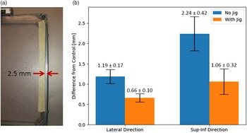
At our cancer centre, a common cause for decommissioning an electron frame is bowing of the frame due to the pressure of the molten alloy against the frame walls. Severe bowing, such as that shown in Figure 6(a), prevents proper insertion of the frame into the applicator. Furthermore, bowing of the frame in the sup-inf direction can cause the cutout encoding to become unreadable, resulting in it being unusable for treatment without a manual override that could compromise patient safety. In our technique, the inner contours of the jig provide structural support to the frame and reduce the potential for bowing. To quantify the bowing for an unsupported frame, molten LMPA was poured into three new 20×20 cm2 frames devoid of cutout negatives, completely filling the frames. When the alloy was cool, it was removed from the interior of the frame and the process was repeated. After the fifth pour, the bowing at the centre of the frame in the x-direction (Left-Right) and y-direction (sup-inf) was measured. The experiment was then repeated using the 3D printed jig. A graph depicting the results for both supported and unsupported frames is shown in Figure 6(b). After five pours, the unsupported frames bowed by 1.19±0.17 mm and 2.24±0.42 mm in the left-right and supinf directions, respectively. In comparison, the corresponding measurements for the frames supported by the 3D printed jig were 0.66±0.10 mm and 1.06±0.32 mm, respectively. These findings demonstrate that use of the 3D printed jig reduces the bowing magnitude by a factor of approximately 2 in both the left-right and sup-inf directions. This, in turn, directly increases the number of patient treatments which can be completed using a single frame, lengthening the frame’s lifetime.
Results of the frame bowing experiments. (a) Example of an insert frame exhibiting extreme warping in the lateral direction, as indicated by the two arrows. There is a 2.5 mm gap between the acrylic base plate indicated with masking tape and the exterior of the frame. (b) A graph summarising the warp test results for frames which were poured with (orange) and without (blue) the 3D printed jig. There is a factor of 1.8 difference between the unsupported and jig supported pours in the lateral direction and a factor of 2.11 difference in the sup-inf direction.

As discussed previously, for a given 3D model, both the print time and the material cost scale with model size. The cost per patient (both in terms of time and money) of any clinical 3D printing technique may thus become a concern for plans which require large field apertures, especially in centres with a high patient load. In this regard, the most expensive print job in this work was the 25×25 cm2 jig, which ran for 10.5 hours and used 388 g of ABS filament. At the time of writing, the cost of printer filament is approximately $30 CAD/kg, hence the monetary cost associated with printing the 25×25 cm2 jig (as determined by the weight of filament used) is slightly less than $12 CAD. In comparison, with the same print settings, the 6×6 cm2 frame was printed in 3 hours and used 116 g of filament, equivalent to a cost of about $3.50 CAD. The jigs themselves only need to be printed once and can be used multiple times until failure, and thus add a monetary cost on the order of tens of cents when considered on a per-patient basis. The time and material costs associated with printing the patient specific negatives are generally significantly less than the costs for the corresponding jig. For example, the patient negatives for the 20×20 cm2 applicator typically require 40 to 50 g of filament and take between 45 minutes and 1.5 hours to print − significantly faster than the 1–9 hours quoted in previous works. Reference Michiels, Mangelschots, Roover, Devroye and Depuydt15 Thus, including the cost of printing the jig, the total estimated monetary cost of this technique (for a centre already equipped with a 3D printer) is approximately $2 CAD per patient.
Conclusion
We have presented a new 3D printing-based method for generating electron aperture blocks. A 3D printer was used to print aperture negatives and an insert frame jig made of ABS, which is resistant to deformation at the high temperatures associated with conventional cadmium-free LMPA. Electron blocks created using the 3D printed negatives produced FWHMs within 1% of those in the associated TPS plan, while the use of the 3D printed jig was found to reduce insert frame bowing by a factor of 2. We further demonstrated the feasibility of generating precise multi-aperture and off-axis electron blocks with the technique; to our knowledge, this is the first time this has been attempted using a 3D printing approach. With the increasing popularity and demonstrated versatility of 3D printers in the field of medical physics, this process is poised to become a viable low-cost alternative to conventional electron block fabrication techniques.