I. INTRODUCTION
Thermoelectrics is not a new topic in the field of materials research, but the increasing utilization of nanotechnological approaches opened the door for a rebirth of the research on thermoelectrics because of new abilities to modify the transport coefficients. Using nanotechnology, there are two different approaches for enhancing the thermoelectric figure of merit

where α, σ, κ, and T are the Seebeck coefficient, the electrical conductivity, the thermal conductivity, and the absolute temperature, respectively. First, the power factor can be increased by exploiting quantum effects on the nanoscale.Reference Majumdar1 Second, well-designed nanostructured materials have the ability to scatter phonons much more effectively than electrons, causing a decrease in lattice thermal conductivity. In an ideal case, lattice thermal conductivity is strongly reduced without influencing the electronic transport properties. For instance, Poudel et al.Reference Poudel, Hao, Ma, Lan, Minnich, Yu, Yan, Wang, Muto, Vashaee, Chen, Liu, Dresselhaus, Chen and Ren2 have managed to increase the thermoelectric efficiency of bismuth antimony telluride (BiSbTe) bulk alloy by introducing additional grain boundaries and defects to the material through nanostructuring. A common approach toward a three-dimensionally nanostructured thermoelectric bulk uses high-energy ball milling followed by compactifying the material under preservation of the nanofeatures, recently reviewed in Ref. Reference Lan, Minnich, Chen and Ren3. Successful optimization of the figure of merit into a technologically relevant range was demonstrated for ball milled and sintered nanocomposites of classical thermoelectric compositionsReference Lan, Minnich, Chen and Ren3 and has recently been realized for a half-Heusler compound, Zr0.5Hf0.5CoSb0.8Sn0.2.Reference Yan, Joshi, Liu, Lan, Wang, Lee, Simonson, Poon, Tritt, Chen and Ren4 Thus, the approach of employing nanostructuring to increase the thermoelectric efficiency allows for an engineering of materials, which combines a high figure of merit and sustainability.
This work will focus on the synthesis of nanoparticles of the well-known alloy Si1-xGex in an up-scalable gas phase synthesis and the application of these engineered nanostructures for thermoelectricity. SiGe has a suitable power factor and also a moderate thermal conductivity. SiGe represents a classic high temperature thermoelectric material, which is found in applications such as space missions, where sunlight is not sufficient as an energy source. Since germanium is an expensive element, a broad mass application on earth is still lacking. However, we will approve our new technology based on this well-known material to gain suitable results and a reasonable database to judge whether our approach vindicates further investigation in gas phase based bottom-up technologies. Besides the disadvantage of high germanium costs, a silicon-based material system for thermoelectric mass application would have the big advantage of a clear margin in processing issues, as industry has already accumulated a broad knowledge on processing silicon-based devices. Furthermore, silicon is a cheap and almost unlimitedly available material. Additionally, in combination with germanium and also in form of silicides it is mostly nontoxic, which is not the case for many of today’s thermoelectric materials, often containing heavy elements like lead, bismuth, or tellurium. Thus, sustainable energy harvesting from waste heat of high temperature processes might be a possible application.
The thermoelectric efficiency of pure silicon is not (yet) sufficient for a lucrative application as thermoelectric generator or peltier cooling device. Nevertheless, Bux et al.Reference Bux, Blair, Gogna, Lee, Chen, Dresselhaus, Kaner and Fleurial5 have improved the thermoelectric figure of merit from 0.2 (found for heavily n-type doped single-crystalline silicon at 900 °C) to 0.7 only by nanostructuring the material. Furthermore, Boukai et al.Reference Boukai, Bunimovich, Tahir-Kheli, Yu, Goddard Iii and Heath6 have reported a zT value of around 1 at 200 K for silicon nanowires caused by phonon effects. However, it is still a big challenge to connect the nanowires with our macroscopic world to benefit from their high efficiency.
Mingo et al.Reference Mingo, Hauser, Kobayashi, Plissonnier and Shakouri7 have shown that an effective reduction of the thermal conductivity can be achieved by a combination of alloying and an additional nanostructure. The homogeneous distribution of elements with different atomic masses within an alloy structure acts as scatter centers for short-wavelength phonons, while the nanostructure with its high concentration of grain boundaries has a major impact on mid- to long-wavelength phonons. Manufacturing nanocrystalline SiGe alloys fulfills both of these principles. Therefore, an improvement of the figure of merit compared to single- or polycrystalline SiGe alloy is expected.
There are some earlier works that have presented nanocrystalline bulk SiGe alloys by using a different manufacturing process. Wang et al.Reference Wang, Lee, Lan, Zhu, Joshi, Wang, Yang, Muto, Tang, Klatsky, Song, Dresselhaus, Chen and Ren8 have obtained a peak zT of 1.3 for nanostructured Si80Ge20 alloys at 900 °C, whereas Zhu et al.Reference Zhu, Lee, Lan, Wang, Joshi, Wang, Yang, Vashaee, Guilbert, Pillitteri, Dresselhaus, Chen and Ren9 could fabricate a nanostructured Si95Ge5 alloy with a performance comparable to that of single-crystalline Si80Ge20 alloy. In both cases, a top-down method starting with bulk raw material using a milling process was used to obtain the nanosized material.
This work introduces a new approach to tailor a nanosized material for the formation of nanostructured thermoelectrics. It is based on the nanoparticle synthesis from gaseous precursors in a gas phase reactor. Most importantly, it enables for an ideal, homogeneous mixture of all components as long as they are available in the form of suitable gaseous precursor materials. Moreover, the composition and even the size and morphology of particles can be tuned in a wide range.Reference Gurav, Kodas, Pluym and Xiong10
II. SYNTHESIS OF SiGe ALLOY NANOPARTICLES FROM THE GAS PHASE
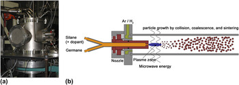
Intense grinding of silicon and germanium bulk material in a milling system can be used to synthesize a nanostructured alloy, in which atoms of one element are more or less statistically replaced by atoms of the other element. In contrast, our approach is the gas phase synthesis. Figure 1(a) shows a photograph of our lab scale reactor. The process is sketched in Fig. 1(b). We start from gaseous precursors and feed them into a low-pressure plasma reactor.Reference Knipping, Wiggers, Rellinghaus, Roth, Konjhodzic and Meier11 In a completely miscible system like SiGe, this usually ends up in a perfect distribution of both elements within the alloy. We used a microwave-induced argon–hydrogen plasma for the thermal decomposition of a precursor mixture consisting of silane (SiH4), germane (GeH4), and phosphine (PH3). Subsequent to the decomposition of the precursors, a silicon/germanium vapor is formed, supersaturating while cooling down when leaving the hot plasma zone. The degree of supersaturation is lowered by nucleation and primary particles are formed, growing by collision, coalescence, and sintering. Growth ends when the vapor is depleted and the temperature has dropped below the particle’s melting point. Accordingly, the particle size is mainly determined by the precursor concentration and by the pressure in the reactor. Due to high temperature gradients in our plasma process, usually spherical and loosely agglomerated particles are formed. To adjust electrical conductivity and Seebeck coefficient, doping of the material is needed. It can be realized by adding an appropriate precursor to the initial gas mixture, as there are diborane (B2H6) for p-type doping and phosphine (PH3) for n-type doping. The particles are filtered from the gas and collected under inert conditions to protect them from contamination and from ambient atmosphere.
Nanoparticle synthesis by a gas phase process. (a) Photograph of a lab scale plasma reactor. (b) Sketch of the particle synthesis: Silane and germane precursors as well as a gaseous precursor for the intended doping are mixed and injected into the plasma zone through a nozzle. After nucleation, nanoparticles grow by collision, coalescence, and sintering.

The gas phase approach used in a lab scale reactor mostly results in particle sizes between 5 and 50 nm while the production rate is up to 10 g/h. Scale-up of the gas phase process is possible in general and well-known, enabling for a production rate at the kilogram per hour scale. We consider this as one important advantage of this gas phase synthesis compared to other manufacturing routes for semiconductor nanoparticles. Tailoring of nanoparticle size, doping concentration, and chemical composition is easily accessible by varying the composition of the precursor gases and tuning pressure or flow rates within the plasma reactor.
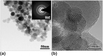
For the particles presented in this work, molar fractions of 79.4 mol% silane, 19.8 mol% germane, and 0.8 mol% phosphine were used to synthesize phosphorus-doped Si80Ge20. A transmission electron microscopy (TEM) image of the as-prepared particles is shown in Fig. 2 indicating spherical, single-crystalline particles.
(a) Transmission electron microscopy (TEM) images of Si80Ge20 alloy nanoparticles synthesized in a microwave plasma reactor. The average diameter is 16 nm. (b) High resolution TEM image shows soft-agglomerated, single-crystalline particles.

III. EXPERIMENTAL
A. Field assisted sintering
For the compaction of the Si80Ge20 nanoparticles, a field assisted sintering technique (FAST) also called spark plasma sintering was used.Reference Munir, Anselmi-Tamburini and Ohyanagi12 Compared to common hot pressing methods, FAST offers the opportunity to obtain dense bulk pellets out of nanoparticles, while the nanocrystallinity is only little affected. We used a sintering machine HP D 40 from FCT Systeme GmbH (Rauenstein, Germany).
About 3 g of as-prepared particles were put into a graphite die coated by a boron nitride layer to ensure that the electrical current flows through the particulate packed bed. A pressure of 35 MPa was applied to the sample while a current of maximum 500 A at 4.5 V was used to heat it up to 1000 °C at a fixed rate of 100 K/min. At 1000 °C, the temperature was kept constant for 3 min and afterwards it was cooled down at the same rate (100 K/min). There are two remarkable densification steps during the sintering process. The first compaction is caused by applying the pressure of 35 MPa, whereas the main compaction occurs within the temperature range between 800 and 1000 °C. This main densification process can be attributed to a partial melting of the nanoparticles as it was shown for silicon nanoparticles.Reference Schierning, Theissmann, Wiggers, Sudfeld, Ebbers, Franke, Witusiewicz and Apel13
Using the FAST setup as described above, coin-like pellets with a diameter of 2 cm and a thickness of about 3 mm are obtained. A typical density of sintered Si80Ge20 from gas phase material was found to be 2.911 g/cm3. This matches with a residual porosity of about 3.3% compared to literature data of dense Si80Ge20 alloy.Reference Dismukes, Ekstrom and Paff14
B. Microstructural analysis
The mean crystallite size of as-prepared and sintered material was obtained from x-ray diffraction (XRD) measurements with subsequent Rietveld refinement using a Siemens D5000 diffractometer (Bruker AXS GmbH, Karlsruhe, Germany) in Debye-Scherrer geometry and combined with Rietveld analysis. The data evaluation was done with the software package fullprof.Reference Rodriguez-Carvajal15 For comparison, the average particle size of the raw powder was also determined by an analysis of the free surface according to the BET method. The measurement was done in a Nova 2200 from Quantachrome (Boynton Beach, FL) using nitrogen as adsorbent.
TEM was used to investigate the structural properties and to determine potential anisotropies resulting from the uniaxial sintering process. Therefore, different slices were cut in parallel and perpendicular to the sintering orientation, grinded down to 50-μm thickness and subsequently thinned to electron transparency by a precision ion polishing system. A 200-keV Tecnai F20 ST (FEI, Eindhoven, Netherlands) equipped with an EDX system and Gatan imaging filter was used for the electron microscopy.
C. Transport characterization
The Seebeck coefficient and the electrical conductivity were measured in the direct setup by means of a ZEM-3 from ULVAC Technologies Inc. (Ulvac GmbH, Garching, Germany), whereas the thermal conductivity was measured by a laser flash method using an LFA 457 Microflash from NETZSCH GmbH (Selb, Germany). The thermal diffusivity was measured directly using the Cape–Lehman fitting model,Reference Cape and Lehman16 and the specific heat capacity was calculated via a pyroceramic reference sample. Due to the sample geometry, thermal characterization was done in direction of the current during sintering, while the electrical properties were measured perpendicularly. Density was obtained exploiting the Archimedes principle by weighing the samples in air and in water.
IV. RESULTS AND DISCUSSION
A. Microstructure
The as-prepared powder from microwave plasma gas phase synthesis consists of mostly single-crystalline, spherical particles with a mean diameter of 16 nm (see Fig. 2), calculated from XRD measurement. Note, that the mean diameter of the raw powder is around 26 nm if analyzed by BET. Generally, BET is sensitive to the free surface of particles and agglomerates, whereas XRD is only sensitive to the size of the smallest single-crystalline unit. The difference in the average diameter obtained by the two different methods is, therefore, an indication for a moderate agglomeration of the raw powder.
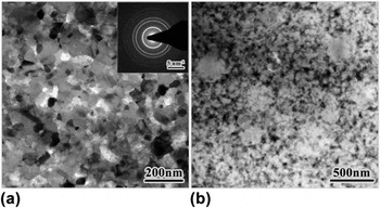
As calculated from the XRD measurements, the mean crystallite size increases to about 32 nm after sintering. Figure 3(a) shows a bright field TEM image of a typical section of the sintered sample, whereas Fig. 3(b) shows a bigger overview by using scanning TEM (STEM). The electron diffraction shown as an inset in Fig. 2(a) affirms the polycrystallinity of the sample, while the average grain size of 32 nm is also verified by the TEM images.
TEM characterization of the sintered Si80Ge20 alloy; (a) bright field TEM image (b) scanning TEM image from the same sample.

The chemical composition of the sintered sample obtained by energy-dispersive x-ray spectroscopy (EDX) is 80.44 ± 0.48 at.% silicon, 18.89 ± 0.51 at.% germanium, and 0.66 ± 0.03 at.% phosphorus. Within the accuracy of this method, it confirms that the composition is almost exactly what was intended from gas phase synthesis. Therefore, it can be stated that the final composition can be adjusted exactly by initially mixing the appropriate amounts of precursors in advance of gas phase formation process.
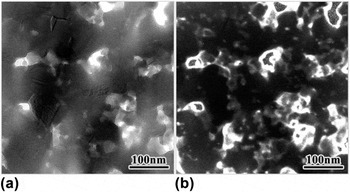
A more detailed investigation of the composition is shown in Fig. 4. Energy-filtered TEM was used to distinguish between silicon and silicon oxide within the sintered pellets. Because the manufacturing process includes some handling steps under ambient conditions, a certain amount of oxygen within the samples cannot be avoided. Therefore, the particles may be covered with some native oxide before being processed by FAST. From detailed investigations on silicon nanoparticle sintering, we know that for sufficiently high temperatures at about 800 °C and above a precipitation of the oxide takes place, also supporting the green body densification.
Energy-filtered measurements of a characteristic section of the sintered sample. (a) Bright field TEM image (b) difference signal of energy-filtered TEM images of silicon plasmon excitation energy and silicon oxide plasmon excitation energy. Silicon-oxide-rich areas appear bright. The dark areas are attributed to pores within the sintered sample.

From Fig. 4(a), it can be seen that certain porosity, indicated by the bright spots, is still present after sintering. This is in accordance with the findings from density measurements, indicating a porosity of 3.3%. Figure 4(b) shows that silicon oxide seems to concentrate at the grain boundaries. Moreover, the difference pattern shown in Fig. 3(b) clearly indicates that silicon oxide precipitates at the internal surface of the pores. As a result, the pores are exclusively located within silicon oxide precipitates, which are supposed to be a direct consequence from the rearrangement of the silicon oxide during the sintering process.
It is also noteworthy to mention that no evidence was found for dealloying of the Si80Ge20 after sintering. Neither in STEM nor in EDX measurements a segregation of germanium could be observed. Hence, we assume that the SiGe alloy structure of the nanoparticles is not affected by the sintering process. Although some FAST-treated phosphorus-doped pure silicon samples sintered at 1060 °C have shown a structural anisotropy in the microstructure resulting from a preferred orientation or melting during sintering,Reference Schwesig, Schierning, Theissmann, Stein, Petermann, Wiggers, Schmechel and Wolf17 within the investigation of Si80Ge20 alloy sintered at 1000 °C no structural anisotropy could be found.
B. Transport properties
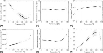
Figure 5 summarizes the different transport properties measured as a function of temperature. As the Seebeck coefficient is directly proportional to the temperature, its absolute value rises as expected from −175 μV/K at room temperature to −326 μV/K at 815 °C. After that peak temperature, it significantly decreases down to −283 μV/K at 960 °C. The electrical conductivity has no specific temperature dependence within the measurement accuracy. Values around 140 S/cm are found with an uncertainty of about 10%. Therewith, a power factor ranging from 5 × 10⁻⁴ to 1.4 × 10⁻³ W/(m·K2) can be calculated.
Temperature dependence of (a) Seebeck coefficient, (b) specific electrical conductivity, (c) power factor, (d) charge carrier concentration, (e) thermal conductivity, and (f) the dimensionless figure of merit zT.

For highly doped (degenerated) semiconductors, the active charge carrier concentration can be calculated directly from the Seebeck coefficient using the equation
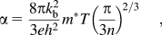
where α is the Seebeck coefficient, n is the charge carrier concentration, e is the charge of an electron, k b is the Boltzmann constant, h is Planck’s constant and m* is the effective mass of the charge carriers. Since Rieger et al.Reference Rieger and Vogl18 have reported that in unstrained Si1-xGex alloys, the effective masses vary only weakly with the composition of the alloy, a Si-like effective mass of m* = 0.92 m 0 was taken for the calculation.Reference Schäffler, Levinshtein, Rumyantsev and Shur19 The result is plotted in Fig. 5(d) indicating an increasing electron concentration with increasing temperature. Nevertheless, the charge carrier concentration is about one order of magnitude lower than expected for a dopant concentration of 0.8% phosphorus. Therefore, we assume that a lot of the dopant added to the gas mixture is not electrically active because of segregation within the oxidic precipitates.Reference Stegner, Pereira, Lechner, Klein, Wiggers, Stutzmann and Brandt20
Compared to results obtained from other groups,Reference Wang, Lee, Lan, Zhu, Joshi, Wang, Yang, Muto, Tang, Klatsky, Song, Dresselhaus, Chen and Ren8 the thermal conductivity of the nanostructured SiGe alloy is surprisingly low with its minimum value of 1.55 W/m-K at around 650 °C. This low value serves as a main reason for a quite reasonable figure of merit of 0.8 ± 0.15 between 720 and 830 °C, which is almost identical to values measured for a radioisotope thermoelectric generator used for National Aeronautics and Space Administration (NASA) space flight with a typical grain size of 1–10 μm.
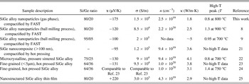
Table I summarizes literature data of SiGe alloys and nanocomposites. It can be seen that our new approach has not yet resulted in record values of ZT, mostly because of unoptimized electronic properties. On the other hand, the measured value of 1.8 W/m-K for the thermal conductivity is much lower than comparable literature data. The alloying as dominant scattering mechanism for short range phonons is expected to be near to ideal as a consequence of mixing the precursors in the gas phase. Long-range phonons are not only scattered at grain boundaries of the nanocomposite but also at oxygen precipitates as shown in Fig. 4. Thus, our results are highly encouraging. First, they show that the new bottom-up approach delivers a comparable performance as the highly engineered NASA material. More importantly, we see a couple of very promising optimization parameters: as can be seen from the charge carrier concentration (Table I), the increase in dopant concentration as well as an increasing activation of dopants is expected to significantly increase the specific electrical conductivity. Utilizing the advantages of homogeneous gas phase synthesis with adjustable ratio of different components will help to optimize composition and dopant concentration. Additionally, we also expect a distinct improvement by optimization of the densification process leading to sintered materials with strongly reduced porosity. Therefore, a main focus will be set to the optimization of the sintering parameters. Future experiments will also address the reduction of the germanium content to maximize the performance to material cost ratio. Last but not least, the upscaling possibility of the nanoparticle synthesis is an important aspect that makes the proposed manufacturing process also highly interesting with respect to industrial utilization, once the parameters are optimized.
Thermoelectric data of n-type SiGe nanocomposites and SiGe alloys. Seebeck coefficient α, electrical conductivity σ, charge carrier concentration n, and thermal conductivity κ are room temperature values. For the peak zT, the temperature is indicated.

FAST, field assisted sintering technique.
V. SUMMARY
A new manufacturing process for nanostructured SiGe alloys was introduced. Homogeneously alloyed SiGe nanoparticles doped with 0.8% phosphorus were synthesized from gaseous precursors in a microwave plasma reactor. The nanoparticles were compacted to almost dense pellets using FAST. During the sintering process, a coarsening of the average particle size from initial 16 nm to a final mean crystallite size of 32 nm was observed. Microstructural analysis reveals no segregation of germanium, thus, indicating that the alloy remains stable during the sintering process. A figure of merit of 0.8 ± 0.15 was found for nanostructured Si80Ge20 alloy fabricated in the presented manner. Hence, it could replicate the figure of merit of Si80Ge20 alloys used for radioisotope thermoelectric generators by the NASA, although our experimental parameters are not yet optimized. Future experiments will address the optimization of doping level and sintering temperature. Moreover, the germanium content will be reduced to maximize performance to material cost ratio.
ACKNOWLEDGMENTS
We thank M. Winterer and D. Gautam, Faculty of Engineering, for the use of the spark plasma sintering machine and M. Farle, Department of Experimental Physics, for the possibility to use the microscopy facilities. Financial supports from the German Research Foundation (Deutsche Forschungsgemeinschaft) within the priority program SPP 1386: Nanostrukturierte Thermoelektrika, the European Union and the Ministry of Economic Affairs and Energy of the State North Rhine–Westphalia in Germany within the frame of an Objective 2 Programme (European Regional Development Fund) are gratefully acknowledged.