Introduction
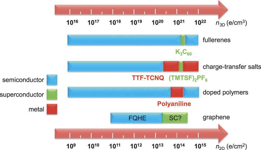
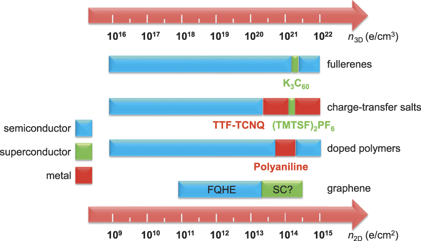
Free charge-carrier density is one of the key parameters controlling the electronic properties and phase behavior of insulators, semiconductors, and superconductors.Reference Ahn, Di Ventra, Eckstein, Frisbie, Gershenson, Goldman, Inoue, Mannhart, Millis, Morpurgo, Natelson and Triscone1 One clear effect of mobile charge density is the giant span of electrical conductivity from metals (∼107 S/m) to insulators (∼10–22 S/m). In organic semiconductors, the role of free-carrier density on electronic properties is not as well understood as it is in more conventional electronic materials.Reference Ahn, Triscone and Mannhart2 In particular, significant charge-carrier correlations can be anticipated in these materials because they are characterized by low dielectric constants (low charge screening) and relatively narrow bandwidths. Figure 1 summarizes the near zero-temperature electronic properties of several prototype organic materials that have been investigated as a function of their free-carrier concentrations. A noteworthy example is C60, which exhibits a superconducting phase when each fullerene molecule is doped by three alkali metal atoms but converts back to a semiconducting/insulating state at higher or lower doping levels.Reference Haddon3 As in other electronically correlated materials, it is clear that systematic control of charge density over a wide range is of great importance to obtain exciting and desirable electronic properties in organic semiconductors.
Illustration of several electronic properties of organic semiconductors near zero temperature as a function of their charge densities. Methods to tune charge densities include chemical doping, field-effect gating, and electrolyte gating. Superconductivity in graphene was predicted theoretically at high charge densities. Examples of organic semiconductors that exhibit novel transport behaviors are also listed. Note: FQHE, fractional quantum Hall effect; SC, superconductor; TTF-TCNQ, tetrathiafulvalene-tetracyanoquinodimethane; (TMTSF)2PF6 (tetramethyltetraselenafulvalene)hexafluorophosphate; n 2D, sheet charge carrier density (cm–2); n 3D, bulk charge carrier density (cm–3).
The electrostatic field-effect approach serves as an ideal technique for controlled and reversible tuning of charge densities without introducing disorder into the active material. In this framework, an external electric field is applied to a semiconductor material across a gate insulator using a gate electrode. This creates a thin accumulation or depletion layer near the surface whose electrical conductivity between source and drain electrodes can be modified systematically by the gate voltage. Current flows when a drain bias is applied, and its magnitude is determined by the standard field-effect transistor (FET) equations as
 $$I_D = {W \over L}\mu V_D C_i (V_G - V_{Th} )$$
 $$I_D = {W \over {2L}}\mu C_i (V_G - V_{Th})^2 ,$$
in which I D is the drain current (A), V D is the drain voltage (V), W and L are channel width and length (μm), respectively, μ is the carrier mobility (cm2 V–1 s–1), C i is the specific capacitance (F/cm2), V Th is the threshold voltage (V), and V G is the gate voltage (V). The total induced charge-carrier density (in cm–2) is controlled through Q = C i(V G–V Th) (C i= εrεo/t i, εr is the dielectric constant of the gate insulator, εo is the vacuum permittivity, t i is the insulator thickness). For the commonly used SiO2 insulator, total charge density is not more than 2 × 1013 cm–2 at best due to its breakdown field E b = 10 MV/cm and εr = 3.9. Several research groups have employed ultrathin self-assembled monolayers (SAMs) or cross-linked polymer films as gate insulators to boost capacitance.Reference Halik, Klauk, Zschieschang, Schmid, Dehm, Schütz, Maisch, Effenberger, Brunnbauer and Stellacci4–Reference Kim, Wang, Choi, Ha, Facchetti and Marks7 Another strategy has been to employ complex oxide ferroelectrics with field-dependent εr near 300 at room temperature.Reference Ahn, Triscone and Mannhart2, Reference Ahn, Gariglio, Paruch, Tybell, Antognazza and Triscone8 Although carrier concentrations near 1014 cm–2 have been realized in the best case outcome in these reports,Reference Halik, Klauk, Zschieschang, Schmid, Dehm, Schütz, Maisch, Effenberger, Brunnbauer and Stellacci4–Reference Ahn, Gariglio, Paruch, Tybell, Antognazza and Triscone8 device fabrication is tedious, and high-charge densities are not easy to achieve under favorable circumstances.
It can be seen from Figure 1 that most of the novel transport phenomena in organic semiconductors, such as metallic transport and superconductivity, occur at sheet charge densities above 1013 cm–2. In recent years, electrolyte gating, that is replacing conventional solid dielectrics (such as SiO2) with electrolyte materials (such as ionic liquids, see below), has emerged as a reliable and effective technique to achieve charge densities in the range of 1013 to 1015 cm–2 with convenient fabrication and easy carrier tunability. Electrolyte gating for high charge density accumulation has facilitated a series of research breakthroughs in fundamental transport in physics-rich correlated electron systems. One example is the observation of superconductivity in SrTiO3 near 1014 cm–2 induced by the field-effect when gated with electrolytes.Reference Ueno, Nakamura, Shimotani, Ohtomo, Kimura, Nojima, Aoki, Iwasa and Kawasaki9 Explorations of novel transport phenomena in organic molecules have also motivated extensive research efforts in understanding the device physics in electrolyte-gated organic semiconductors and particularly in organic crystals. In the following, we summarize recent research highlights in fundamental aspects of electrolyte-gated organic crystals. We present the general techniques of how to apply electrolytes as a high-capacitance insulator, how to determine the key figures of merits (such as charge density), and how several exciting achievements are expected to ultimately lead to even broader breakthroughs. Applications of electrolyte gating in printed and flexible electronics are reviewed elsewhere.Reference Kim, Hong, Lee, Xie, Zhang, Lodge and Frisbie10
Mechanism of electrolyte gating
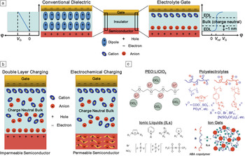
Figure 2a illustrates the working mechanism of electrolyte-gated organic field-effect transistors (OFETs).Reference Kim, Hong, Lee, Xie, Zhang, Lodge and Frisbie10 Take p-type semiconductors as an example. With application of negative gate voltage, cations in the electrolyte can migrate toward a gate/electrolyte interface to compensate electric charges in the gate electrode, while anions will move to the electrolyte/semiconductor interface. Holes are therefore induced in the semiconductor channel to balance the ionic charges. The interfacial layers of ions and countercharges are referred to as electrical double layers (EDLs). The novelty of this polarization process is that the gate potential is only dropped at the EDLs, over about 1 nm distance, while the bulk region of the electrolyte remains charge neutral and field-free. As a result, the capacitance associated with the electrolyte gating is enormous, on the order of μF/cm2, facilitating accumulation of charge-carrier densities above 1013 cm–2 with only a few volts operation. Transistors based on this type of mechanism are referred to as electrical double layer transistors (EDLTs), and charge accumulation is via two-dimensional double layer charging (electrostatic field-effect) (Figure 2b). In this scenario, the active semiconductors are typically single crystalline, such that electrolyte ions and charge carriers can closely pack at the interface to form double layers. Electrolyte-gated organic single-crystal FETs are thus considered EDLTs.
Modes of electrolyte gating and materials. (a) Cross-sectional schematic of gate-insulator-semiconductor structure in field-effect transistor geometry for conventional solid dielectrics and electrolyte gates. Polarization occurs through the bulk of the conventional dielectric layer, while for electrolyte gates, gate potential is only dropped at the double layers over 1 nm distance. (b) Charge accumulation mechanism in the modes of double layer charging (electrostatic) and electrochemical charging. (c) Various types of electrolyte materials for studies of transport physics in organic crystals at high charge densities. Note: ϕ, electric potential; V ref, reference voltage; V G, gate voltage; EDL, electrical double layer; R, R1, R2, R3, various alkyl groups; n, the number of repeating units in a polymer chain.

The aforementioned situation may change if the semiconductor is permeable to ions, such as conjugated polymer thin films. The conduction happens when anions penetrate into the film during oxidation of the p-type semiconductor or cations during reduction of the n-type semiconductor. The charge accumulation is reversible upon removal of gate bias, as counterions move into the film to balance the ionic charge and restore the semiconductor to its neutral state. This type of device is regarded as an electrochemical transistor (Figure 2b), and charge accumulation is through three-dimensional electrochemical doping. Electrolyte-gated polymer thin-film transistors (TFTs), for instance, belong to this category. Electrochemical operation very likely introduces more structural disorder into the semiconductor layer compared with electrostatic EDL charging.
Figure 2c shows a few commonly used electrolyte materials that have been paired with organic single crystals and thin films. One of the earliest and most extensively studied solid electrolyte materials is poly(ethylene oxide) (PEO) doped with a lithium salt (e.g., LiClO4).Reference Panzer and Frisbie11 In this electrolyte, the oxygen lone pairs on the flexible PEO chains coordinate with the Li+ cations, resulting in a coupled ion motion along the polymer backbone. Another interesting class of solid electrolytes is polyelectrolytes, or polymers with substituents along the backbone containing ionic functionalities.Reference Herlogsson, Noh, Zhao, Crispin, Sirringhaus and Berggren12 The special characteristic of polyelectrolytes is that only one ionic species (cation or anion) is mobile, while the counterion is a fixed polymer chain. This feature proves useful in controlling the polarity of conduction (electron or hole) in organic thin-film transistors (OTFTs). More recently, ionic liquids (ILs) and ionic liquid-based gels have been employed.Reference Ye, Craciun, Koshino, Russo, Inoue, Yuan, Shimotani, Morpurgo and Iwasa13–Reference Cho, Lee, Xia, Kim, He, Renn, Lodge and Frisbie15 ILs consist of highly mobile ions without any solvent, similar to sodium chloride in molten state. ILs also show a unique combination of properties, such as excellent thermal and electrochemical stability, negligible volatility, and high ionic conductivity. Particularly, the former two properties make ILs exceptional as high capacitance dielectrics in transistors for a variety of low-temperature transport studies, as discussed later. A widely used class of IL includes imidazolium-based cations (e.g., 1-ethyl-3-methylimidazolium [EMI]) with various anions such as tetracyanoborate (TCB) and bis(trifluoro-methylsulfonyl)imide (TFSI). Ion gels, on the other hand, comprise a cross-linked polymer network (e.g., polystyrene-poly(methyl methacrylate)-polystyrene [PS-PMMA-PS] block copolymer) swollen with an IL (e.g., EMI, TFSI) such that high capacitance and high ionic conductivity are maintained, but mechanical integrity is greatly improved.Reference Lodge16 The availability of all these electrolyte materials provides broad options for fabricating high-performance electrolyte-gated EDLTs.
Determination of charge density and carrier mobility
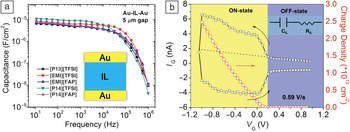
Determination of charge density and carrier mobility in electrolyte-gated organic single crystals is not trivial. Unlike conventional dielectrics, where the capacitance is equal to the ratio of dielectric permittivity to layer thickness ( $C_i = {{\varepsilon _r \varepsilon _o } \mathord{\left/ {\vphantom {{\varepsilon _r \varepsilon _o } {t_i }}} \right. \kern-\nulldelimiterspace} {t_i }}$), the capacitance of an electrolyte layer is a function of both operating frequency and gate voltage due to the double layer nature at the electrolyte/semiconductor interface. Several techniques have been developed to address the issue of determining charge density. One is to directly measure the capacitance as a function of frequency (C–f) or gate voltage (C–V) using the AC impedance technique. A broadband impedance analyzer or an LCR (impedance-capacitance-resistance) bridge is commonly used in this type of measurement. One can use the capacitance measured at low frequencies (close to DC limit) to extract carrier mobility from Equation 1 or 2. Figure 3a shows an example of a C–f plot for several ILs tested in a metal-insulator-metal (MIM) structure, with low-frequency capacitance approaching 10 μF/cm2.Reference Xie and Frisbie17 Otherwise, capacitance can be measured versus gate voltage at low frequencies, and charge density can then be obtained by integrating capacitance versus gate voltage, following
 $p = \int {{\raise0.7ex\hbox{${C_i }$} \!\mathord{\left/ {\vphantom {{C_i } e}}\right.\kern-\nulldelimiterspace}\!\lower0.7ex\hbox{$e$}}} dV_G $, where p is total charge density (cm–2) and e is elementary charge (1.6 × 10⁻¹⁹C). Carrier mobility can then follow
 $${\rm{\mu }} = {L \over W}{{I_D } \over {V_D ep}}.$$
Determination of capacitance and charge density. (a) Capacitance-frequency relationship for several ionic liquids (ILs) in an Au-IL-Au structure at room temperature. The specific capacitance of these ILs reaches 10 μF/cm2 at the low frequency limit (10 Hz), much larger than for conventional dielectrics (e.g., 35 nF/cm2 for 100 nm SiO2). (b) Gate displacement current I G taken at a particular sweep rate (0.59 V/s) in ionic liquid gated rubrene electrical double layer transistors. The black dotted line represents the integration background. The inset shows the equivalent circuit model for the double layer structure. Because of the large capacitance of ILs, a charge density of 2.5 × 1013 cm–2 is achieved at a gate voltage of only –1 V. See Figure 4b for device structure. Reproduced with permission from Reference Reference Xie and Frisbie17. © 2012 American Chemical Society. Note: I G, gate displacement current; V G, gate voltage; CIL, the capacitive part of a metal-IL-metal structure; RIL, the resistive part of a metal-IL-metal structure; [EMI], 1-ethyl-3-methyl imidazolium; [P13], 1-propyl-1-methyl pyrrolidinium; [P14], 1-butyl-1-methyl pyrrolidinium; [TFSI], bis(trifluoromethylsulfonyl)imide; [FAP], tris(pentafluoroethyl)trifluorophosphate.

An alternative technique is to measure the gate displacement current while sweeping the gate voltage, with source and drain contacts grounded. Similar to the process of charging/discharging an ideal capacitor and measuring the charging/discharging current, the displacement current trace can be divided into regions of opening (ON-state) and closing (OFF-state) of the conductive channel. Figure 3b shows one example of a gate displacement current plot in an IL-gated rubrene EDLT. The forward sweep corresponds to charge injection (charging a capacitor), and the reverse sweep corresponds to charge retraction (discharging a capacitor). Charge density is determined by integrating the displacement current of the forward sweep with respect to the gate voltage via
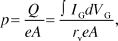 $$p = {Q \over {eA}} = {{\int {I_G dV_G } } \over {r_V eA}}$$
where I G stands for the gate displacement current (A), r v is the gate voltage sweep rate (dV G/dt) (V/s), and A is the active channel area (cm2). The integration baseline is usually assigned as the OFF-state current trace (the dotted line in Figure 3b). The displacement current measurement is therefore a quasi-static DC measurement and is expected to approach the capacitance measurement at low frequencies but deviate at the high-frequency limit. Both techniques have been successfully applied to determine the charge densities in electrolyte-gated organic single crystals.Reference Xie and Frisbie17
The Hall effect is a classical method to measure the free charge-carrier density in metals and semiconductors, but application of the Hall effect to OFETs is challenging due to the general low carrier mobility (below 1 cm2 V–1 s–1) for most organic semiconductors. Only in recent years have Hall measurements been carried out in high mobility p- and n-type organic crystals for transport studies.Reference Podzorov, Menard, Rogers and Gershenson18, Reference Minder, Ono, Chen, Facchetti and Morpurgo19 Using the Hall effect to measure charge density above 1013 cm–2 in organic EDLTs would be extremely interesting; however, there are no such reports to date. One challenge is that carrier mobility decreases strongly once the dielectric is changed from low-εr dielectrics (such as vacuum gap with εr = 1) to electrolytes that have a typical εr above 10 due to the coupled polaronic effect between carriers and dielectric environment.Reference Xia, Cho, Lee, Ruden and Frisbie14 Nevertheless, by carefully selecting the electrolyte material with a larger-sized anion (namely, tris(pentafluoroethyl)trifluorophosphate, or FAP), carrier mobility in rubrene EDLTs reached 3.2 cm2 V–1 s–1.Reference Xie and Frisbie17 It is therefore not too ambitious to envision Hall measurement on organic EDLTs for direct measurement of high charge densities in the near future.
Progress in organic single-crystal EDLTs
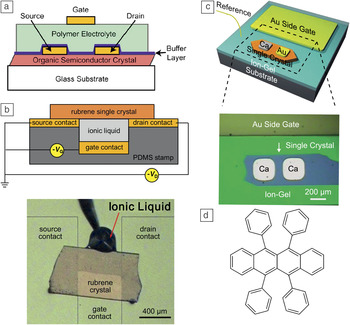
Depending on the choice of electrolyte material used, various methods of fabricating organic single-crystal-based EDLT devices are available, as shown in Figure 4. Generally, the fragile organic single crystals are first carefully laminated on a particular substrate such as a piece of silicon wafer or a poly(dimethylsiloxane) (PDMS) rubber stamp. In the case of polymer electrolytes (Figure 4a), a top-contact top-gate geometry has been adopted, and the electrolyte can be directly drop cast and cured on the crystal surface.Reference Panzer and Frisbie20 However, due to the presence of the solvent, a thin buffer layer is needed between the crystal and electrolyte to ensure functioning and reproducible devices. Use of solvent-free ILs does not impose such concerns of degrading crystal surfaces. One could simply put a drop of IL on top of the crystals and insert a metal wire/mesh into the liquid as the gate electrode.Reference Ono, Seki, Hirahara, Tominari and Takeya21 Otherwise, to confine the liquid within the channel area, the pioneering idea of laminating crystals on a PDMS rubber substrate to form vacuum-gap transistors can be borrowed.Reference Menard, Podzorov, Hur, Gaur, Gershenson and Rogers22 Instead of a vacuum dielectric, ILs are filled into the channel beneath the crystal by capillarity such that a clean liquid/crystal interface could be formed (Figure 4b).Reference Xia, Cho, Lee, Ruden and Frisbie14 In another strategy (Figure 4c), a thin smooth layer of ion gel has been spun cast before lamination of crystals on top.Reference Yomogida, Pu, Shimotani, Ono, Hotta, Iwasa and Takenobu23 Symmetric or asymmetric contacts are then evaporated on the crystal surface by the shadow mask technique. Whichever fabrication method is employed, a high-quality smooth electrolyte/crystal interface needs to be realized for a high-performance EDLT device.
Electrical double layer transistor (EDLT) device structures. (a) Device structure of organic crystals gated with a polymer electrolyte. Reproduced with permission from Reference Reference Panzer and Frisbie20. © 2006 American Institute of Physics. (b) Schematic (top) and optical micrograph (bottom) of ionic-liquid gated rubrene EDLT on a polydimethylsiloxane (PDMS) rubber substrate. Reproduced with permission from Reference Reference Xia, Cho, Lee, Ruden and Frisbie14. © 2009 Wiley. (c) Schematic (top) and optical image (bottom) of ion-gel gated ambipolar single crystal EDLT. Either symmetric (e.g., Ca-Ca) or asymmetric (e.g., Au-Ca) contacts can be employed in this structure. Reproduced with permission from Reference Reference Yomogida, Pu, Shimotani, Ono, Hotta, Iwasa and Takenobu23. © 2012 Wiley. (d) Molecular structure of rubrene. Note: V G, gate voltage; V D, drain voltage.

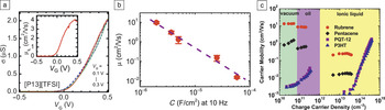
Extensive growth and characterization of organic single crystals started in the early 1950s and has thrived again over the past decade.Reference Sundar, Zaumseil, Podzorov, Menard, Willett, Someya, Gershenson and Rogers24 Electrolyte gating of organic crystals, however, first appeared only a few years back. The benchmark organic material, rubrene single crystal (molecular structure shown in Figure 4d), which exhibits room temperature hole mobility above 10 cm2 V–1 s–1, has been gated with polymer electrolytes in several reports.Reference Panzer and Frisbie20, Reference Shimotani, Asanuma, Takeya and Iwasa25 Due to the high capacitance of the electrolytes used (above 10 μF/cm2), devices are operated with a few volts of gate voltage, and enormous hole densities (estimated from the capacitance of the electrolyte measured in a MIM structure) of about 1013 cm–2 to 1015 cm–2 are achieved. The clear advantage of electrolytes for high charge density accumulation is evident by comparison with SiO2 gated devices (C i∼10 nF/cm2) in which gate voltages larger than 10 V are applied, but maximum charge density is only one-tenth of the charge achieved in electrolyte gates. Other p-type (e.g., pentacene) and n-type (e.g., tetracyanoquinodimethane [TCNQ], N,N”-bis(n-alkyl)-(1,7 and 1,6)-dicyanoperylene-3,4:9,10-bis(dicarboximide)s [PDIF-CN2]) crystals have been investigated with ionic liquid gates.Reference Panzer and Frisbie20, Reference Uemura, Yamagishi, Ono and Takeya26, Reference Ono, Minder, Chen, Facchetti and Morpurgo27 Specifically, Ono et al.Reference Ono, Minder, Chen, Facchetti and Morpurgo27 reported electron mobility up to 5 cm2 V–1 s–1 in IL-gated PDIF-CN2 single-crystal transistors (Figure 5a), a value that is comparable to the highest electron mobility in the same material with poly(methyl methacrylate) (PMMA) gates.Reference Molinari, Alves, Chen, Facchetti and Morpurgo28
Progress in single-crystal electrical double layer transistors (EDLTs). (a) Channel conductance (σ) as a function of gate voltage (V G) in an ionic liquid (IL)-gated N,N′-bis(n-alkyl)-(1,7 and 1,6)-dicyanoperylene-3,4:9,10-bis(dicarboximide) (PDIF-CN2) EDLT. Calculated electron mobility (μIL) as a function of V G is included in the inset. This device exhibits the highest electron mobility (4 cm2 V–1 s–1) in organic single crystals when gated with an electrolyte. The IL used in this study is [P13][TFSI] ([1-propyl-1-methyl pyrrolidinium][bis(trifluoromethylsulfonyl)imide]. Reproduced with permission from Reference Reference Ono, Minder, Chen, Facchetti and Morpurgo27. © 2010 American Institute of Physics. (b) Mobility (μ)-capacitance (C) relationship in rubrene EDLTs gated with various types of ILs that have different capacitance values. The dashed line is a linear fit of a μ-C relation in the log-log plot. A clear trend of decreasing mobility with increasing IL capacitance can be observed, similar to the observation in Reference Reference Hulea, Fratini, Xie, Mulder, Iossad, Rastelli, Ciuchi and Morpurgo30 when the gate insulators are conventional dielectrics. Reproduced with permission from Reference Reference Ono, Miwa, Seki and Takeya29. © 2009 American Institute of Physics. (c) Comparison of carrier mobility-charge density (μ-p) relationship in vacuum-gap and liquid-gated single crystals versus polymer thin films. The large span of charge density comes from the large difference in the capacitance of vacuum (∼0.18 nF/cm2), silicone oil (∼0.55 nF/cm2), and IL (∼15 μF/cm2). Single crystals and polymer thin films exhibit distinct μ-p behaviors due to the different states of disorder. P3HT, poly(3-hexylthiophene); PQT-12, poly(3,3’’’-didodecylquarterthiophene). Reproduced with permission from Reference Reference Xia, Cho, Lee, Ruden and Frisbie14. © 2009 Wiley.

More detailed transport studies have been carried out mostly on rubrene crystals gated with ILs on PDMS stamp substrates. Ono et al. measured the carrier mobility in rubrene gated with various types of ILs that exhibit different capacitance values (Figure 5b).Reference Ono, Miwa, Seki and Takeya29 A decrease of mobility with increasing capacitance was shown, a trend similar to that discovered a few years earlier in rubrene crystals gated with solid dielectrics.Reference Hulea, Fratini, Xie, Mulder, Iossad, Rastelli, Ciuchi and Morpurgo30 Frisbie and co-workers systematically compared the transport in rubrene single-crystal and poly(3-hexylthiophene) (P3HT) thin-film transistors with vacuum gap and liquid gates, such that gate-induced charge densities were tuned over a large range from 1010 cm–2 to 1013 cm–2.Reference Xia, Cho, Lee, Ruden and Frisbie14 A striking difference in the carrier mobility-charge density (μ-p) relationship was reported (Figure 5c). For single crystals of rubrene, the carrier mobility was not a strong function of charge density, but depended strongly on the dielectric constant (capacitance) of the insulator in keeping with previous results from Ono and Morpurgo.Reference Ono, Miwa, Seki and Takeya29, Reference Hulea, Fratini, Xie, Mulder, Iossad, Rastelli, Ciuchi and Morpurgo30 On the other hand, for a polymer semiconductor such as P3HT that had more significant disorder than single crystals, carrier mobility increased strongly with increasing carrier concentration due, perhaps in part, to the continuous filling of trap states. Employing different gate dielectrics, including high capacitance ILs, was therefore able to reveal dramatically distinct transport behavior in single crystals versus thin films due to different states of disorder.
A limitation of operating organic EDLT devices is the finite electrochemical window of the electrolytes. That is, significant redox reaction at the electrolyte/crystal interface may happen if the applied gate voltage is beyond a certain range. For example, at room temperature, the operating voltages of single crystal EDLTs reported are typically not higher than –2 V to prevent irreversible device degradation.Reference Shimotani, Asanuma, Takeya and Iwasa25–Reference Ono, Minder, Chen, Facchetti and Morpurgo27 This problem can be overcome by decreasing the temperature at which the device is operated, such that the electrochemical activity of the electrolyte is greatly suppressed. Another apparent advantage is that a larger gate voltage can be applied before device breakdown, resulting in potentially even higher charge densities. ILs meet the need of a low melting point (T m), but, more importantly, even if the ILs are in their glassy state, ions are still mobile for effective charge-carrier accumulation. Therefore, IL-gated EDLTs can be operated at temperatures down to the glass transition temperatures (T g). For 1-ethyl-3-methylimidazolium bis(trifluoromethylsulfonyl)imide ([EMI][TFSI]), T m = 258 (K) and T g= 181 (K).Reference Zhang, Lu, Zhou and Li31
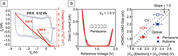
Frisbie and co-workers took advantage of lowering the temperature in EDLTs gated with ILs for high density charge accumulation in rubrene.Reference Xie and Frisbie17 The obtained maximum charge density reached 0.33 holes per rubrene molecule (6.3 × 1013 cm–2) at V G = –3.5 V at 210 K with a 1-butyl-1-methylpyrrolidinium tris(pentafluoroethyl)trifluorophosphate ([P14][FAP]) gate, confirmed by displacement current measurements (Figure 6a). In the same report, the authors also carried out a systematic transport study of rubrene EDLTs gated with various ILs.Reference Xie and Frisbie17 Carrier mobility at room temperature up to 3.2 cm2 V–1 s–1 was achieved by choosing the appropriate type of IL, and it was speculated that if gated with an even larger-sized anion, carrier mobility in rubrene could be further improved (as discussed later). Displacement current and C–V measurements were employed to obtain consistent results of gate-induced hole densities of (2.0∼3.5) × 1013 cm–2 at room temperature. The temperature dependence of carrier mobility exhibited a thermally activated behavior (i.e., mobility decreased with decreasing temperature), which was consistent with prior results obtained by the same group.Reference Xia, Cho, Lee, Ruden and Frisbie14 As a result of high-capacitance liquid gates, the rubrene channel conductivity obtained was as high as 120 S/cm, comparable to the conductivity in doped conductive polymers and organic charge-transfer salts.Reference Cohen, Coleman, Garito and Heeger32, Reference Chiang, Fincher, Park, Heeger, Shirakawa, Louis, Gau and MacDiarmid33
Progress in single-crystal electrical double layer transistors (EDLTs). (a) High charge density accumulation in an IL-gated rubrene EDLT at 210 K. Maximum attainable hole density at 210 K is 6.3 × 1013 cm–2, corresponding to 0.33 holes per rubrene molecule. This doubles the maximum amount of charge obtained at 300 K, as seen from the red lines. At 210 K, three displacement current sweeps (sweep rate 0.12 V/s) that are scanned to different gate voltages are plotted, shown as the black (to V G = –1.5 V), green (to V G = –2.5 V), and blue (to V G = –3.5 V) curves. The dotted line is the integration background. Note: I G, gate displacement current; V G, gate voltage. Reproduced with permission from Reference Reference Xie and Frisbie17. © 2011 American Chemical Society. (b) Ambipolar transport of ion-gel gated pentacene EDLT (left) and correlation between bandgap energies determined from cyclic voltammetry (CV)/optical absorption and summation of electron/hole threshold voltages for pentacene (red circle) and rubrene (blue square) crystals (right). Open symbols stand for cyclic voltammetry, and filled symbols stand for optical absorption measurement. The black dashed line corresponds to a slope of one, and the gray dashed lines are a guide for the eyes. The threshold voltages of holes and electrons in single-crystal ambipolar EDLTs offer a new method to investigate HOMO-LUMO gap energies of the materials. Reproduced with permission from Reference Reference Yomogida, Pu, Shimotani, Ono, Hotta, Iwasa and Takenobu23. © 2012 Wiley. Note: HOMO, highest occupied molecular orbital; LUMO, lowest unoccupied molecular orbital; V Th, threshold voltage; V D, drain voltage.

High charge densities with electrolyte gates have also been used to induce ambipolar transport in rubrene crystals (i.e., both holes and electrons are accumulated in the channel). Takenobu reported ion-gel gated rubrene and pentacene single-crystal ambipolar transistors that were operated in the sub-3V regime (Figure 6b).Reference Yomogida, Pu, Shimotani, Ono, Hotta, Iwasa and Takenobu23 A spin-cast molecularly flat ion gel film was used to gate organic crystals with symmetric (either Au or Ca) or asymmetric (Au-Ca) contacts. Significantly, the summation of electron and hole threshold voltages corresponded with the bandgaps of respective molecules, indicating a new method for investigating HOMO-LUMO gap energies of organic materials. Light-emitting ion-gel gated organic crystal EDLTs were also anticipated with further optimizations of device performance, for the purpose of ultimately realizing electrically driven organic lasers.Reference Yomogida, Pu, Shimotani, Ono, Hotta, Iwasa and Takenobu23
Conductivity peak at high charge densities
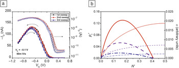
A remarkable observation in rubrene crystals gated with electrolytes is that the channel conductivity exhibits a pronounced peak at a certain gate voltage (charge density) (i.e., a negative transconductance). This behavior, which is independent of IL composition and is not an artifact of contact effect or gate leakage, appears at charge densities around (1.5 ∼ 2.5) × 1013 cm–2 (0.1 holes per rubrene molecule).Reference Xie and Frisbie17, Reference Xia, Xie, Ruden and Frisbie34 As seen from Figure 7a, the stable and reproducible EDLT performance also implies that a high-quality rubrene/liquid interface is maintained. In fact, the occurrence of conductivity peaks is not uncommon in electrolyte-gated organic thin-film transistors.Reference Panzer and Frisbie11, Reference Ofer, Crooks and Wrighton35–Reference Paulsen and Frisbie37 However, ion penetration in organic films is very likely to occur, which introduces extra complexity in understanding this unusual behavior. On the other hand, a conductivity peak is not observed in electrolyte-gated inorganic semiconductors such as ZnO when induced charge densities are in the vicinity of 1015 cm–2.Reference Yuan, Shimotani, Tsukazaki, Ohtomo, Kawasaki and Iwasa38
Unusual conductivity behavior. (a) Transfer characteristics (drain current I D-gate voltage V G) of IL-gated rubrene electrical double layer transistors. Drain voltage V D is –0.1 V, and the sweep rate is 50 mV/s. A pronounced peak in channel current (conductivity) is clearly observed. The IL used in this study is [P13][TFSI] ([1-ethyl-1-methyl pyrrolidinium][bis(trifluoromethylsulfonyl)imide]. Reproduced with permission from Reference Reference Xie and Frisbie17. © 2011 American Chemical Society. (b) Model results for the normalized mobile hole density, p ′f (thin lines, left scale), and the conductivity (σ) (bold lines, right scale) as a function of the normalized ion density N’. The solid lines are for F = 0.1, the dashed lines are for F = 0.01, and the dash-dotted lines are for F = 0.001, where F is defined as the ratio of trap emission to the capture coefficient. Larger F values imply a smaller degree of carrier trapping. Reproduced with permission from Reference Reference Chiang, Fincher, Park, Heeger, Shirakawa, Louis, Gau and MacDiarmid33. © 2010 American Physical Society.

Ruden et al. proposed a two-dimensional percolative transport model to explain the peak conductivity in rubrene crystals based on the fact that rubrene has a low dielectric constant (εr ∼ 3) and a narrow HOMO bandwidth (∼0.5 eV).Reference Xia, Xie, Ruden and Frisbie34 As a result, the binding interaction between anions and holes at the rubrene/electrolyte interface is so strong that carrier localization occurs, leading to a decrease in carrier mobility. The model results are shown in Figure 7b, in which the free charge densities tend to saturate with increasing ion density (higher V G), indicating the trapping of carriers. A decrease in mobility compared to the bulk mobility is also inherently predicted by this model. The authors speculated that the lowering of effective carrier mobility was a general phenomenon in any narrow band, low εr semiconductor at high charge densities. However, the mobility lowering effect might be tuned or mitigated by employing a large-sized anion to reduce the ion-binding interaction, as revealed by several studies of IL-dependent mobility.Reference Xie and Frisbie17, Reference Ono, Miwa, Seki and Takeya29 In spite of these exciting findings, further studies are required to better understand the conductivity behavior and mobility lowering effect at high charge densities.
Summary and outlook
We have reviewed research developments in electrolyte-gated, highly charged organic single crystals at charge densities above 1013 cm–2 and have suggested why these efforts have the potential for a broader and more significant impact in the near future. Recent progress on high-performance single-crystal electrical double layer transistor devices were summarized, including ambipolar transport, large hole and electron mobility (3∼5 cm2 V–1 s–1), high charge density (6.3 × 1013 cm–2), and, more intriguingly, a pronounced conductivity peak. We also provided a detailed introduction to the working mechanism of the electrolyte gating process, electrolyte materials, and techniques to measure gate-induced charge densities. Although this is a young area of research, this field has seen a variety of exciting achievements that are key steps toward understanding the charge transport in organic crystals at high charge density. These research efforts are important for ongoing efforts to realize novel transport behavior in organic crystals (e.g., superconductivity and the insulator-to-metal transition) in the high charge density regime.
Acknowledgments
All work done at the University of Minnesota was supported by the MRSEC program of the National Science Foundation under award number DMR-0819885. We thank Prof. P. Paul Ruden (University of Minnesota), Dr. Yu Xia (Polyera Corporation), and Dr. Shimpei Ono (Central Research Institute of Electric Power Industry) for valuable discussions.