I. INTRODUCTION
The materials on the ternary phase-diagram of GeSbTe show an extraordinary combination of physical properties: many of these alloys can be switched rapidly and reversibly between their amorphous and crystalline phases, having large differences in optical reflectivity or electrical resistivity, but at the same time remain remarkably stable at room temperature. Reference Ovshinsky1–Reference Loke, Lee, Wang, Shi, Zhao, Yeo, Chong and Elliott4 It is for these reasons that phase-change materials (PCMs) of GeSbTe alloys (bulk GeSbTe), most notably Ge2Sb2Te5, have been applied in optical recording media like rewritable disks, and are currently intensely investigated for next-generation nonvolatile electronic memories Reference Raoux, Burr, Breitwisch, Rettner, Chen, Shelby, Salinga, Krebs, Chen, Lung and Lam5,Reference Burr, Breitwisch, Franceschini, Garetto, Gopalakrishnan, Jackson, Kurdi, Lam, Lastras, Padilla, Rajendran, Raoux and Shenoy6 and opto-electronic applications. Reference Hosseini, Wright and Bhaskaran7–Reference Ríos, Hosseini, Taylor and Bhaskaran9 Moreover, PCMs have recently attracted scientific interest due to the occurrence of a controlled insulator–metal transition upon annealing the crystalline phase, which is shown to be of an Anderson (and not Mott) type. Reference Siegrist, Jost, Volker, Woda, Merkelbach, Schlockermann and Wuttig10 This makes GeSbTe based PCMs also an interesting platform for fundamental studies on transport and charge localization.
For PCM electronic memories one of the major drawbacks is the large programming current (I prog) which is needed for reset switching (i.e., amorphization) of the material. The reason is that I prog is coupled to the memory's crystalline resistance (R set) in an inversely proportional way, typically I prog ∼ R set −1, which particularly becomes important as the devices are being scaled to lower dimensions. Reference Lacaita and Redaelli11,Reference Boniardi, Redaelli, Cupeta, Pellizzer, Crespi, D'Arrigo, Lacaita and Servalli12 A breakthrough in the field occurred when Chong et al. and later Simpson et al. showed that thin films consisting of GeTe–Sb2Te3 multilayers and superlattices, produced in rather different ways, have significantly reduced I prog compared to bulk GeSbTe, as well as new and better switching properties. Reference Chong, Shi, Zhao, Tan, Li, Lee, Miao, Du and Tung13,Reference Simpson, Fons, Kolobov, Fukaya, Krbal, Yagi and Tominaga14 Chong et al. initially proposed that the reduced programming current originates from the lower thermal conductivity of the super-structure. However, this suggestion was disputed for the epitaxial films with much thinner GeTe sublayers in the work by Simpson et al., referred to as interfacial phase-change memory (iPCM), who showed using pump-probe thermoreflectivity that this conductivity was actually higher for superlattices than for bulk GeSbTe. This led the authors to seek an explanation in terms of a crystal–crystal transition in iPCM, Reference Tominaga, Fons, Kolobov, Shima, Chong, Zhao, Lee and Shi15,Reference Tominaga, Shima, Fons, Simpson, Kuwahara and Kolobov16 skipping the costly amorphization step (via the molten state), and thereby reducing I prog.
Despite these advances, the structural models and resistance-switching mechanism of iPCM are not clearly understood and different theories are debated in the literature. In this work, as well as in previous publications, Reference Momand, Wang, Boschker, Verheijen, Calarco and Kooi17–Reference Wang, Bragaglia, Boschker and Calarco19 we critically analyze the atomic structure of epitaxial GeTe–Sb2Te3 superlattice PCMs with special attention to (i) ordering and mixing of Ge and Sb and (ii) the formation of so-called vacancy layers and van-der-Waals (vdW) bonds. Using both molecular beam epitaxy (MBE) and sputtering physical vapor deposition (PVD) various superlattice films were grown and characterized with high-resolution (HR) transmission electron microscopy (TEM), high-angle annular dark field scanning TEM (HAADF-STEM), TEM energy dispersive x-ray spectroscopy (EDX), and x-ray diffraction (XRD). Contrary to the proposed models in the field of iPCM, it is found that the separate binary compounds intermix and actually form superlattices of Sb2Te3 and GeSbTe vdW layers, as would be expected based on the structural models by Kooi et al. Reference Kooi and Hosson20 and Matsunaga et al. Reference Matsunaga and Yamada21–Reference Matsunaga, Kojima, Yamada, Kifune, Kubota and Takata23
II. CRYSTAL STRUCTURES OF GeTe, Sb2Te3 AND GeSbTe
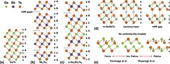
To better understand the properties and the proposed resistance-switching mechanisms of GeTe–Sb2Te3 superlattices, as well as PCMs on the GeTe–Sb2Te3 tie-line, it is necessary to study the crystalline structure and bonding of the ternary as well as the separate binary compounds. Figures 1(a)–1(c) show the structural models of GeTe, Sb2Te3 and the stable phase of Ge2Sb2Te5 (s-Ge2Sb2Te5) according to Goldak et al., Reference Goldak, Barrett, Innes and Youdelis24 Anderson et al., Reference Anderson and Krause25 and Kooi et al., Reference Kooi and Hosson20 respectively. As can be seen in the figures, all structures are based on consecutive abc-stacking of close-packed atomic planes. Within a simplified picture, GeTe is a three-dimensionally (3D) bonded solid which has approximately a rocksalt structure that is rhombohedrally and ferroelectrically distorted along one of the four 〈111〉 directions (c > a√6 and z = 0.237, where c = a√6 and z = 0.250 for the rocksalt structure). Sb2Te3 on the other hand has an additional feature of directly adjacent Te–Te planes stacked upon each other, which breaks the rocksalt symmetry by breaking the super-ABC stacking of the Te planes. This happens since Sb has one extra valence electron, and because of this the bonds on the outer Te planes are passivated and form two-dimensional (2D) vdW bonds. This type of vdW bond, which also occurs in e.g., graphene-based materials and transition-metal di-chalcogenides, Reference Geim and Grigorieva26 is referred to as vdW gap. Note that, although Sb2Te3 has certainly a more 2D than 3D anisotropy, the Te–Te bond does not necessarily have to be of pure vdW type (e.g., the Te–Te interatomic distance is a bit smaller than what would be expected based on the vdW radius Reference Matsunaga and Yamada21–Reference Matsunaga, Kojima, Yamada, Kifune, Kubota and Takata23 ). Considering the above, the model for s-Ge2Sb2Te5 by Kooi et al. takes into account this 3D and 2D character of GeTe and Sb2Te3, respectively, and fitted best to experimental electron diffraction results at that time. Reference Kooi and Hosson20
Structural models for crystalline phases of GeSbTe, displayed along hexagonal axes (a-axis horizontal and c-axis vertical). The unit cells are indicated with thin solid lines. (a) GeTe. (b) Sb2Te3. (c) Stable phase of Ge2Sb2Te5 (s-Ge2Sb2Te5). (d) Metastable phase of GeSbTe (m-GeSbTe) with comparison of vacancy layers and vdW gaps. (e) iPCM switching models using single or double Ge umbrella flip. Reference Tominaga, Kolobov, Fons, Nakano and Murakami33,Reference Ohyanagi, Kitamura, Araidai, Kato, Takaura and Shiraishi34 Note that the switch between the different structures cannot only result from a vertical motion, since this would disagree with the abc-stacking. Reference Yu and Robertson35

When GeSbTe crystallizes from the amorphous phase, it initially forms a metastable rocksalt structure (m-GeSbTe), where one sublattice is fully occupied with Te and the other sublattice is randomly occupied by Ge, Sb and a large amount of stoichiometric vacancies (∼20% for Ge2Sb2Te5), Reference Yamada and Matsunaga27,Reference Wuttig, Lüsebrink, Wamwangi, Wełnic, Gilleßen and Dronskowski28 see Fig. 1(d). To make the transition from m-GeSbTe to s-GeSbTe it has been suggested that the mechanism involves atomic diffusion of Ge and Sb in such a way that the vacancies order in layers and consequently collapse into vdW gaps. Reference Matsunaga and Yamada21,Reference Bragaglia, Arciprete, Zhang, Mio, Zallo, Perumal, Giussani, Cecchi, Boschker, Riechert, Privitera, Rimini, Mazzarello and Calarco29 Note particularly the difference in stacking between vacancy layers and vdW gaps in Fig. 1(d). An appreciable amount of disorder on the Ge/Sb planes nevertheless remains after this transition: even though the structure of s-GeSbTe best fits the model of Kooi et al. with Sb–Te directly at the vdW gaps, it was found by Matsunaga et al. using Rietveld refinement on XRD spectra that the Ge-rich planes are mixed with Sb and Sb-rich planes with Ge. Reference Matsunaga and Yamada21–Reference Matsunaga, Kojima, Yamada, Kifune, Kubota and Takata23 In later ab-initio studies relating to the ordering of vacancies it was indeed found that the pure atomic-plane model by Kooi et al. gives the lowest formation energy (at zero Kelvin), but that mixing only slightly increases this energy. Reference Zhang, Thiess, Zalden, Zeller, Dederichs, Raty, Wuttig, Blügel and Mazzarello30 Therefore, due to this low energy increase and the free energy decrease due to configurational entropy, which becomes increasingly relevant at higher temperatures, the stable phase of bulk GeSbTe is always found with some degree of mixing on the Ge/Sb atomic planes (at practical temperatures particularly dictated by production), but with the Sb-rich planes nearest to the vdW gaps.
For GeTe–Sb2Te3 superlattices the separate binary compounds are deposited alternatingly, which hypothetically could produce pure atomic planes. In addition, since Sb2Te3 grows in entire 1 nm quintuple layer (QL) terraces, Reference Jiang, Sun, Chen, Wang, Li, Song, He, Wang, Chen, Xue, Ma and Zhang31 preferring to form layers with passive vdW surfaces, it could be possible to isolate ultra-thin GeTe layers between the vdW surfaces of Sb2Te3. In combination with the research on superlattices and understanding of the role of Ge atoms in PCM phase-transitions, Reference Kolobov, Fons, Frenkel, Ankudinov, Tominaga and Uruga32 it was proposed that the iPCM resistance-switching phase-transition is entirely within the crystalline state. Reference Tominaga, Fons, Kolobov, Shima, Chong, Zhao, Lee and Shi15,Reference Tominaga, Shima, Fons, Simpson, Kuwahara and Kolobov16 Two alternative mechanisms were derived by competing groups based on the Ge-umbrella-flip models, illustrated in Fig. 1(e). Tominaga et al. proposed a single Ge atomic-plane flip between the Ferro and inv. Petrov states, Reference Tominaga, Kolobov, Fons, Nakano and Murakami33 while Ohyanagi et al. proposed a double Ge atomic-plane flip between the Petrov and inv. Petrov states. Reference Ohyanagi, Kitamura, Araidai, Kato, Takaura and Shiraishi34 In later ab-initio simulations, Yu and Robertson showed that such a transition could not result from exclusive vertical motion of Ge atoms and suggested detailed pathways for the transition to occur. Reference Yu and Robertson35 In this work, the structure of GeTe–Sb2Te3 superlattices will be scrutinized also to examine whether it is possible to grow pure atomic planes and to trap GeTe layers between the vdW surfaces of Sb2Te3 and also to test whether the switching mechanisms of Tominaga et al. or Ohyanagi et al. can hold.
III. RESULTS
A. MBE grown superlattices
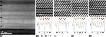
Figure 2 shows HAADF-STEM micrographs with corresponding intensity linescans of a [GeTe(1 nm)–Sb2Te3(3 nm)]15 superlattice, produced at 230 °C with MBE. It has been shown in our previous publications that this film has a well-defined and stoichiometrically consistent superlattice structure. Reference Momand, Wang, Boschker, Verheijen, Calarco and Kooi17,Reference Casarin, Caretta, Momand, Kooi, Verheijen, Bragaglia, Calarco, Chukalina, Yu, Robertson, Lange, Wuttig, Redaelli, Varesi, Parmigiani and Malvestuto18 The film is grown on Sb-passivated Si(111) which makes vdW epitaxy between Si and Sb2Te3 possible. Reference Boschker, Momand, Bragaglia, Wang, Perumal, Giussani, Kooi, Riechert and Calarco36 This type of surface promotes high-quality crystalline growth with strong substrate-film alignment, even though the close-packed planes of Si and Sb2Te3 have an ∼11% mismatch (see also Sec. III. D.). Since HAADF-STEM is an incoherent dark-field imaging technique, the intensity can directly be correlated with the scattering and the images show Z-contrast. So, the Si substrate at the bottom of (a) appears darkest, followed by the bright Sb monolayer and subsequent bright GeSbTe film.
HAADF-STEM results of MBE grown [GeTe(1 nm)–Sb2Te3(3 nm)]15 superlattice on Si(111)-Sb. Above the intensity scans it is indicated whether the atomic plane is Ge-, Sb- or Te-rich with circles, triangles and squares, respectively. (a) Overview image of the superlattice. (b) 5-layers corresponding to Sb2Te3. (c) 7-layer. (d) 11-layer. (e) 13-layer.

In the image of the film dark lines in-between the atomic planes can be observed, which can be associated with vdW gaps and they typically occur between Sb2Te3 QLs. These QLs, also shown in (b), make it possible to distinguish the Sb2Te3 sublayers and they are therefore roughly indicated with the arrows in (a). However, in addition to these QLs one can also find more odd-numbered 7- to 13-layered vdW stacks like shown in (c)–(e). Inspecting the corresponding intensity linescan of each layer system and taking into account the structural models in Fig. 1, it is found that the intensity lowering, i.e., the planes where Ge atoms are intercalated, is happening particularly near the center of the vdW layers and that the Sb-rich planes are always near the vdW gaps. This is indicated with the circles, triangles and squares above the peaks of the linescans (b)–(e). The finding implies that, even though Sb2Te3 growth occurs in single QL steps with passive Te surfaces, GeTe intermixes to a lower energy structure consisting of Sb2Te3 and s-GeSbTe vdW layers. Note that the Sb planes in the s-GeSbTe layers have lower intensity than in Sb2Te3 layers, which happens due to mixing with Ge. Moreover, the growth and vdW bond formation has an inherent asymmetry due to the kinetics, as also pointed out by Wang et al. Reference Wang, Bragaglia, Boschker and Calarco19 When the topmost layer is Sb2Te3, which grows in terraces of entire QLs, GeTe is intermixed within this vdW system. However, when the topmost layer is GeTe, less intermixing occurs to form the Sb–Te termination that is establishing the vdW bond.
In addition, stacking faults and layering disorder occur in the film, which is best seen by the 2- or 4-layered stacking faults in between the odd-layered vdW systems in the film in Fig. 2(a). This is indicative of growth roughness, which is an inherent experimental feature of the growth of these materials. These stacking faults are also another indication that the film has a strong tendency to reconfigure itself. All these findings of the formed vdW layers and defects are fully consistent with the models for s-GeSbTe as proposed by Kooi et al. and Matsunaga et al. Hence, the ground state crystal structure of GeTe–Sb2Te3 superlattices is actually better described as vdW heterostructures of Sb2Te3 and s-GeSbTe.
B. PVD grown superlattices
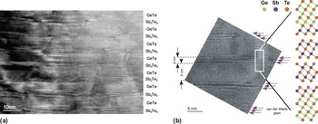
PVD is another technique for film-growth with the advantage that it is adopted much more easily in an industrial process than MBE. Beside this, most of the previous results in the literature have been achieved using PVD grown GeTe–Sb2Te3 films. Reference Chong, Shi, Zhao, Tan, Li, Lee, Miao, Du and Tung13,Reference Simpson, Fons, Kolobov, Fukaya, Krbal, Yagi and Tominaga14,Reference Tominaga, Kolobov, Fons, Nakano and Murakami33,Reference Ohyanagi, Kitamura, Araidai, Kato, Takaura and Shiraishi34 Figure 3 shows (coherent) HRTEM micrographs of a [GeTe(4 nm)–Sb2Te3(3 nm)]15 superlattice, produced at 210 °C with PVD. The film is grown on H-passivated Si(111) which is the surface formed after an HF treatment of the substrate. Also in this case a strong substrate-film alignment occurs, as will be shown in more detail below. HRTEM has a different contrast mechanism than HAADF-STEM because the images are formed through coherent interference of electrons (phase contrast) and this makes interpretation typically more difficult and not directly Z-sensitive. However, due to the dimensionality difference of GeTe and Sb2Te3 it is still possible to distinguish the QLs, and sometimes 7-layers, within the film as can be observed in Fig. 3(a).
HRTEM results of PVD grown [GeTe(4 nm)–Sb2Te3(3 nm)]15 superlattice on Si(111)-H. (a) Overview image of the superlattice. (b) High-resolution image of the superlattice. The model for the structure that is formed is indicated on the right of the image.

Figure 3(b) shows a close-up micrograph of the sublayers that are formed, which seem to disagree with the intended GeTe(4 nm)–Sb2Te3(3 nm) thicknesses. The GeTe sublayer appears to be 5 nm, while only 2 nm (2 QLs) of Sb2Te3 are observed. The bilayer thickness is also verified with EDX, which resulted on average in 29.2 ± 0.5 at.% Ge, 15.3 ± 0.7 at.% Sb and 55.5 ± 0.9 at.% Te. This is equivalent to 61.6 ± 0.9 at.% Ge47Te53 and 38.4 ± 0.7 at.% Sb2Te3, where GeTe is a bit off-stoichiometric due to the inherent presence of ∼10% vacancies on the Ge lattice. Reference Kolobov, Tominaga, Fons and Uruga37 Using these compositional results and the fact that the ∼110 nm film is highly textured along the c-axis, which allows using the literature distances for GeTe (0.356 nm/bilayer), Sb2Te3, (0.1015 nm/QL) and s-GeSbTe, it is calculated that the film on average contains 4.3 nm GeTe and 2.7 nm Sb2Te3. So since 2 nm of Sb2Te3 have formed 5-layered vdW systems (QLs) the remaining amount of Sb is used in the termination of the GeTe sublayers, which is needed to form the vdW bond, as illustrated by the model in Fig. 3(b) on the right. Therefore, also these results of thicker GeTe–Sb2Te3 superlattices produced by sputtering clearly support the formation of s-GeSbTe with mixed Sb-rich planes next to the vdW gap.
C. Thermal stability of GeTe–Sb2Te3 superlattices
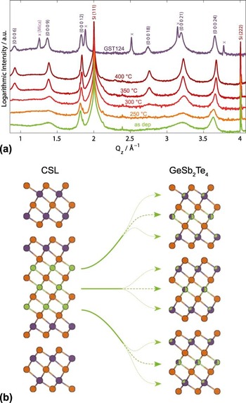
The study of the thermal stability of the superlattices is important because (i) it is argued that there is a thermodynamic tendency to form isolated GeTe blocks within Sb2Te3 at elevated temperatures Reference Tominaga, Kolobov, Fons, Nakano and Murakami33,Reference Yu and Robertson35,Reference Tominaga, Kolobov, Fons, Wang, Saito, Nakano, Hase, Murakami, Herfort and Takagaki38 and (ii) for industrial applications the material has to be able to withstand a certain amount of thermal processing. Beside this, growth at elevated temperatures above ∼200 °C is required for textured growth to occur. Reference Simpson, Fons, Kolobov, Fukaya, Krbal, Yagi and Tominaga14 As it was already shown above, that for growth around ∼230 °C the separate binary compounds intermix by terminating the GeTe blocks with Sb–Te vdW surfaces, it is interesting to know what the further development is at higher temperatures. To examine this a set of [GeTe(1 nm)–Sb2Te3(3 nm)]15 superlattices were prepared on Si(111)-H with PVD at 210 °C and capped with ZnS:SiO2 (80:20) to prevent preferential evaporation of GeTe during annealing. Additionally a GeSb2Te4 film was grown from a stoichiometric target at 320 °C on mica substrates for comparison of the overall structure. Figure 4(a) shows the θ−2θ XRD results of the as-deposited and 250, 300, 350 and 400 °C annealed films.
XRD results of thermal annealing experiments with PVD grown [GeTe(1 nm)–Sb2Te3(3 nm)]15. (a) θ–2θ scans of the superlattice at different temperatures in comparison with GeSb2Te4 which is directly deposited on Mica (top scan). The results clearly indicate that the superlattice structure thermally reconfigures into bulk GeSb2Te4 after 350 °C. (b) Illustration of the structural models for the [GeTe(1 nm)–Sb2Te3(3 nm)] superlattice (CSL) (left) Reference Momand, Wang, Boschker, Verheijen, Calarco and Kooi17,Reference Casarin, Caretta, Momand, Kooi, Verheijen, Bragaglia, Calarco, Chukalina, Yu, Robertson, Lange, Wuttig, Redaelli, Varesi, Parmigiani and Malvestuto18 which reconfigures into the stable phase of bulk GeSb2Te4 (right). Reference Matsunaga and Yamada21

The as-deposited film clearly shows superlattice peaks at Q z = 1.816 Å−1 and Q z = 3.635 Å−1, as well as the 250 °C annealed film which hardly changed the as-deposited structure. However, new and distinct peaks of equally spaced Q z appear after annealing temperature of 350 °C, which further develop at 400 °C. Comparing the positions as well as the intensities of all peaks with the GeSb2Te4 film on mica, it becomes apparent that the superlattice has reconfigured into s-GeSb2Te4, as is schematically illustrated in Fig. 4(b). This finding for the present PVD grown films is fully consistent and in line with the previously obtained results for the MBE grown ones. Reference Momand, Wang, Boschker, Verheijen, Calarco and Kooi17 It implies that the intermixing of GeTe and Sb2Te3 to form s-GeSbTe is a thermodynamic tendency and that this becomes more pronounced at higher annealing or deposition temperatures such that the superlattice feature is lost after 30 min. annealing at 350 or 400 °C. This outlines a delicate thermal balance which has to be achieved during growth: the temperature has to be high enough to favor texture of the superlattice material, but at the same time it has to be low enough to maintain sharp interfaces. Moreover, this shows that the superlattice materials have a limited thermal budget which they can handle, which has to be taken into account for potential industrial implementation. Overall, these findings thus disagree with the previously mentioned ab-initio results Reference Tominaga, Kolobov, Fons, Nakano and Murakami33,Reference Yu and Robertson35,Reference Tominaga, Kolobov, Fons, Wang, Saito, Nakano, Hase, Murakami, Herfort and Takagaki38 and suggest that configurational entropy due to mixing, particularly of the Ge/Sb atomic planes, has to be taken into account for the modeling.
D. Surface preparation
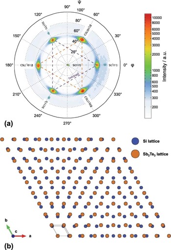
An important prerequisite for the growth of GeTe–Sb2Te3 superlattices is the ability to achieve a film with large domains and a sharp texture due to a single [0001] out-of-plane orientation of the trigonal structure, which typically occurs at deposition temperatures above ∼200 °C. Reference Simpson, Fons, Kolobov, Fukaya, Krbal, Yagi and Tominaga14 Also here, several theories exist on what is the best way to achieve this based on the chemistry of the relevant materials. Reference Boschker, Momand, Bragaglia, Wang, Perumal, Giussani, Kooi, Riechert and Calarco36,Reference Saito, Fons, Kolobov and Tominaga39 Since Sb2Te3 is a 2D bonded component of the film, preferring to organize itself in entire QLs, it becomes natural to exploit this property using vdW epitaxy. Reference Koma40 This approach has the additional advantage that the lattice-matching condition is much more relaxed than for 3D epitaxy, as the chemical bonding on the surface is much weaker. This is the reason why in the above experiments either Si(111)-Sb and Si(111)-H surfaces have been applied. Using these passive surfaces and the Sb2Te3 starting layer, it is possible to grow highly textured and substrate-oriented films. Reference Boschker, Momand, Bragaglia, Wang, Perumal, Giussani, Kooi, Riechert and Calarco36 Figure 5(a) shows an experimental XRD pole figure of the Si(111)-H PVD grown superlattice from Fig. 3 along the {01–12} peak family (conducted at 2θ = 29.80° or |Q| = 2.098 Å−1). From the figure it is clear that the superlattice not only has an excellent out-of-plane alignment, but it is also in-plane aligned with the Si substrate. Since the crystal structure of the superlattice is trigonal, the hexagonal pattern is the result of crystal twinning (60° or 180° rotation around the [0001] i.e., perpendicular to the interface). This epitaxy is schematically illustrated (by a simplified geometric model, excluding potential matching strains which will be small for this vdW-like epitaxy) in Fig. 5(b), where the last (111) plane of Si and the first Te plane of an Sb2Te3 quintuple relative to the interface are overlaid on top of each other.
Epitaxial matching between Si(111) and GeTe–Sb2Te3 superlattices. (a) XRD pole figure of the Si(111)-H PVD grown superlattice showing the {01–12} peak family (conducted at 2θ = 29.80° or |Q| = 2.098 Å−1). The result shows that the superlattice not only has a good out-of-plane alignment, but it is also in-plane aligned with the Si substrate. Since the crystal structure of the superlattice is trigonal, the hexagonal pattern is the result of crystal twinning. (b) Schematic overlay of the nearest close-packed planes of the Si and Sb2Te3 lattices, illustrating the dominant epitaxial relationship according to (a).

Thus, a significant feature for lateral Sb2Te3 growth is that the starting surface is passive, but also smooth, which does not imply that the surface has to be crystalline. This is shown for PVD grown Sb2Te3 layers on the native oxide of the Si substrate. Figure 6(a) shows a part of the film where the native oxide is relatively flat and therefore the quintuple structures of Sb2Te3 can properly organize. This happens during growth initiation to minimize dangling bond surfaces and maximize the passive vdW surface. However, if the surface is rough, tilted domains can form and are observed; see an example shown in Fig. 6(b). The tilt occurs because the initial QLs are formed with a tilt on the rough surface and this is a further seed for subsequent growth. Therefore, the surface roughness is of crucial importance for the growth of superlattices, consistent with the findings by Saito et al., Reference Saito, Fons, Kolobov and Tominaga39 who suggest a way to achieve it with ion-polishing (to produce an amorphous Si surface). Still, in the work of Saito et al. it is claimed that high quality lateral growth also requires materials at the surface that have preference to bond to Te and not Sb. In this respect silicon oxide would not be a suitable surface. However, the present work shows, as has also been pointed out by Ross et al., Reference Ross, Lotnyk, Thelander and Rauschenbach41 that it is nevertheless possible to achieve lateral Sb2Te3 growth on SiO2 directly, indicating that it is rather the surface chemistry than bulk chemistry which is dominant for growth.
Sb2Te3 films grown with PVD on the native oxide of Si(100). (a) Part of the film which shows good out-of-plane alignment due to the smooth SiO2 starting surface. This can be seen since the vdW gaps of Sb2Te3 are aligned parallel to the interface. (b) Part of the film which shows a tilted domain, recognized by the tilted vdW gaps of Sb2Te3, which has formed on a rough part of the substrate.

IV. DISCUSSION
In the above results it is shown that for both MBE and PVD grown superlattices the separate binary GeTe and Sb2Te3 layers intermix. This implies that part of the Sb2Te3 sublayer is used to terminate the GeTe blocks to form passive vdW surfaces. When approaching the ultrathin GeTe limit, this type of surface termination thus naturally forms s-GeSbTe blocks, of which an example is shown in Fig. 1(c) for s-Ge2Sb2Te5. Therefore, these findings implicate that the ground state of GeTe–Sb2Te3 superlattices is best described as a superstructure, i.e., a vdW heterostructure, of Sb2Te3 and s-GeSbTe. In addition, it has been shown through annealing experiments that GeTe–Sb2Te3 intermixing becomes more favorable upon higher temperature. This can even reconfigure the superlattice films entirely into bulk s-GeSbTe if the deposition or annealing temperature is sufficiently high (e.g., 400 °C). Thus, this is an important constraint which is put on growth and processing of the GeTe–Sb2Te3 superlattices, both in terms of film production as well as industrial implementation (which requires heating for several other processing steps).
The proposed ground state for GeTe–Sb2Te3 superlattices, a vdW heterostructure of s-GeSbTe and Sb2Te3, is contradictory to the modeled structures proposed in the literature, Reference Tominaga, Kolobov, Fons, Nakano and Murakami33,Reference Ohyanagi, Kitamura, Araidai, Kato, Takaura and Shiraishi34,Reference Tominaga, Kolobov, Fons, Wang, Saito, Nakano, Hase, Murakami, Herfort and Takagaki38 where it is suggested that GeTe can be isolated within the vdW surfaces of Sb2Te3 layers. The implication of this is that the proposed switching mechanisms, as illustrated in Fig. 1(e), cannot hold or cannot present the complete picture, because they require the previously mentioned condition of GeTe directly adjacent to neighboring Te planes which in principle are the vdW gaps. A possible reason for these discrepancies in the modeling could be the assumption that all structural models consist of pure atomic planes. The work on bulk GeSbTe by Matsunaga et al., Reference Matsunaga and Yamada21–Reference Matsunaga, Kojima, Yamada, Kifune, Kubota and Takata23 already showed that this assumption is incorrect. Therefore, these ab-initio simulations omit the important contribution of configurational entropy to the free energy. This contribution becomes more important at higher temperatures, which are within the growth/annealing regime under consideration. In addition, the switching models here are always considering only 2 GeTe bilayers. Reference Tominaga, Kolobov, Fons, Nakano and Murakami33,Reference Ohyanagi, Kitamura, Araidai, Kato, Takaura and Shiraishi34,Reference Tominaga, Kolobov, Fons, Wang, Saito, Nakano, Hase, Murakami, Herfort and Takagaki38 This is a tough experimental challenge as in practice one always has to take into account roughness, as shown in the current results, and GeTe re-evaporation which is present at higher temperatures. Reference Katmis, Calarco, Perumal, Rodenbach, Giussani, Hanke, Proessdorf, Trampert, Grosse, Shayduk, Campion, Braun and Riechert42,Reference Perumal43 Since it is shown that the superlattices operate at higher sublayer thicknesses of 4 GeTe bilayers, Reference Simpson, Fons, Kolobov, Fukaya, Krbal, Yagi and Tominaga14 it remains unclear how the switching mechanisms generalize to these conditions.
Therefore, it is debatable whether the proposed switching mechanisms in the literature are correct and can explain the properties of GeTe–Sb2Te3 superlattices. A possible alternative, as also pointed out in our previous work, Reference Momand, Wang, Boschker, Verheijen, Calarco and Kooi17 relates to the conventional amorphous-crystalline phase transition of ultrathin GeSbTe layers clamped in the Sb2Te3 matrix. However, one still has to explain the reduced energy consumption which is found in this material. One aspect that is reviving is the improved thermal efficiency (due to the many interfaces) of the superlattice compared to bulk GeSbTe. Such a reduction in thermal conductivity as compared to the constituent materials and also the alloyed compound appears to be a fingerprint of superlattice structures and is also reported in chemically similar systems such as Sb2Te3–Bi2Te3 Reference Venkatasubramanian44 or PbTe–PbTe0.75Se0.25. Reference Caylor, Coonley, Stuart, Colpitts and Venkatasubramanian45 Moreover, as also pointed out previously, a possible solution could lie in the strain which is built up in the sublayers, as can be deduced from the a-lattice constants of GeTe, s-Ge3Sb2Te6, s-Ge2Sb2Te5, s-GeSb2Te4, Sb2Te3 which are a = 0.417, 0.421, 0.422, 0.423, 0.426 nm, respectively. Reference Matsunaga and Yamada21–Reference Anderson and Krause25 Such distortions may add to the total energy of the crystal and thereby lower the amorphization energy, Reference Kolobov, Krbal, Fons, Tominaga and Uruga46 while the faster crystallization dynamics could be explained by templated growth. Reference Simpson, Fons, Kolobov, Krbal and Tominaga47 This type of strain engineering is being suggested by Simpson et al., who propose to use an Sb2Te spacer instead of Sb2Te3. Reference Zhou, Kalikka, Ji, Wu, Song and Simpson48 Because of the larger strain due to the larger a-constant of Sb2Te the memory cells showed even lower energy consumption.
V. CONCLUSIONS
In this work it is shown that the ground state of GeTe–Sb2Te3 superlattices is actually better described as a vdW heterostructure of Sb2Te3 and stable GeSbTe, irrespective of the growth method (MBE or sputtering). The formation of the stable GeSbTe blocks like the one shown in Fig. 1(c), occurs due to the tendency of GeTe to intermix with Sb2Te3 and thereby form passivated vdW surfaces. This type of surface appears to be energetically more favorable over surfaces containing dangling bonds, which is why it seems not possible to obtain isolated blocks of GeTe between Sb2Te3. In addition, it has been shown that intermixing is a thermodynamic tendency which becomes stronger for higher temperatures. This highlights the delicate thermal balance which has to be achieved during growth: the temperature should be sufficiently high to have high-textured crystalline growth but not so high to prevent bulk intermixing and alloying.
The experimental results in this work are thus in striking contradiction with some of the ab-initio results by Tominaga et al. and Ohyanagi et al., which argue that intermixing of GeTe and Sb2Te3 is weaker for higher deposition temperatures. In addition, this type of modeling only takes into account structures with pure atomic planes, omitting the important contributions due to configurational entropy to the free energy of GeSbTe at higher temperatures. Because of this it seems unlikely that the proposed structural models of GeTe–Sb2Te3 superlattices form experimentally and thus that the proposed switching mechanisms are correct. Therefore it becomes necessary to revise the switching model of the GeSbTe superlattices taking into account Sb-rich (instead of Ge) planes near the vdW gaps.
The study of GeTe–Sb2Te3 interfaces in addition provides a versatile platform for the study of the physical phenomena in GeSbTe alloys, such as the formation of vacancy layers, vdW bonds and the related metal-insulator transition which occurs due to ordering. It shows the interplay of different bonding dimensionalities which is tunable within GeSbTe. Overall, the present results have important implications for the understanding of the bonding in GeTe–Sb2Te3 superlattices which are shown to be a new type of nanostructured PCMs.
VI. METHODS
The MBE growth procedure is detailed in our previous publications. Reference Momand, Wang, Boschker, Verheijen, Calarco and Kooi17,Reference Casarin, Caretta, Momand, Kooi, Verheijen, Bragaglia, Calarco, Chukalina, Yu, Robertson, Lange, Wuttig, Redaelli, Varesi, Parmigiani and Malvestuto18 PVD films were grown from stoichiometric GeTe and Sb2Te3 targets by MaTeck (Juelich, Germany, 3 inch, purity 99.99%). The sputter-guns were powered by 35 W with an Ar flow of 35 sccm yielding a deposition pressure of p = 1.6 × 10⁻² mbar (pd = 0.28 mbar cm with d ≈ 17.5 cm the deposition distance). The substrates have been thermalized for 30 min at the deposition temperature (210 °C) prior to deposition. Annealing of films was performed in a tube furnace, where heating and cooling occurred at 5 K/min and held at constant temperature for 30 min under constant Ar flow of 150 sccm.
TEM specimen were prepared by mechanical polishing, dimple-grinding and low-voltage Ar+ ion-milling with a Gatan PIPS II (Gatan Inc., Pleasanton, California). HAADF-STEM measurements were performed with a JEOL ARM 200F (JEOL Ltd., Tokyo, Japan) with sub-Å settings, where the accelerating voltage was 200 kV, the semi-convergence angle was 22 mrad and ADF collecting angles were 68–280 mrad. The (coherent) TEM measurements were performed with a JEOL 2010F (JEOL Ltd.) and EDX measurements were performed with a JEOL 2010 (JEOL Ltd.) equipped with LN2-cooled SiLi detector.
XRD measurements were conducted on a Bruker D8 Discover (Bruker Corporation, Billerica, Massachusetts). θ–2θ scans were performed with a Ge(220) ACC2 monochromator (provided by Bruker Corporation) and a 0.6 mm detector slit. Pole figure measurements were conducted in skew geometry without detector slits.
Structural models in Fig. 1 are drawn with the VESTA software package. Reference Momma and Izumi49
ACKNOWLEDGMENTS
This work was supported by EU within the FP7 project PASTRY (GA 317746). Solliance is acknowledged for funding the HRSTEM facility.