Introduction
Graphene is a single-atomic-layer honeycomb lattice of carbon atoms in a sp 2-hexagonal bonding configuration. Carbon nanotubes (CNTs) are essentially cylinders rolled from graphene sheets with a variety of chiralities depending on the direction of rolling to the hexagonal lattice. These unique structures give CNTs and graphene many fascinating properties, including special electrical properties, excellent mechanical strength, high thermal conductivity, and flexibility. Chemical vapor deposition (CVD) is the most widely used method for the growth of CNTs and graphene. It provides the ability to obtain high-quality and structure-controlled production of CNTs and graphene. Hundreds of tons of CNTs and thousands of square meters of graphene films are produced worldwide each year by CVD. Reference Jia and Wei1 The commercial-scale production and affordable prices make many commercial applications achievable, including additives in rechargeable batteries, automotive parts, and sporting goods. Most exciting is the fact that single-wall carbon nanotubes (SWCNTs) and graphene are being commercialized for electronic applications. In this article, we review the important milestones in the applications of CNTs and graphene. The key characteristics and advantages of CNTs and graphene for specific applications are compared, and future trends are discussed.
Electronics and optoelectronics based on CVD-grown CNTs and graphene
Nanoelectronics
Graphene’s unique electronic properties give it great potential for ultrahigh-speed electronics. High carrier mobility field-effect transistors (FETs) have been widely investigated with graphene as channel materials. In principle, the high mobility allows faster switching circuits, and the ideal two-dimensional (2D) structure enables ultimate scaling of the device channel. However, unlike transistors with conventional semiconductor channels, a graphene FET cannot be completely switched off, since graphene is intrinsically a semimetal with a zero bandgap. As a result, graphene FETs cannot be directly used for digital logic applications. Although a bandgap can be opened by forming narrow ribbons to introduce quantum confinement in graphene, Reference Han, Ozyilmaz, Zhang and Kim2 the manufacture of narrow graphene nanoribbons remains a challenge, especially by CVD. Furthermore, bandgap opening in a graphene nanoribbon increases the effective mass of charge carriers, Reference Raza and Kan3 which decreases its mobility.
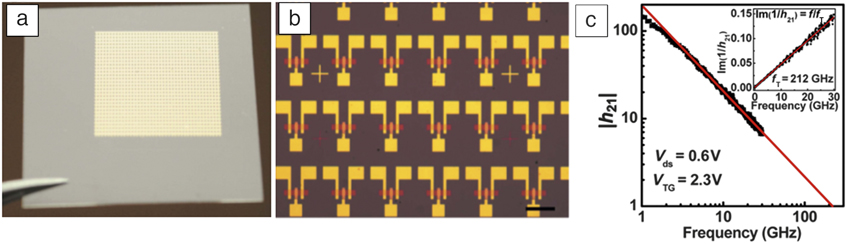
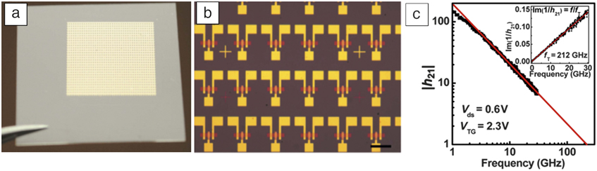
On the other hand, in analog circuits, the ability to completely switch off devices is not necessary. As a result, graphene is well suited for fast analog electronics, especially for radio-frequency transistors, which can be used in AC voltage amplifiers, audio amplifiers, and frequency multipliers for wireless communication. Using CVD-grown graphene, IBM scientists have fabricated a graphene FET on a diamond-like carbon substrate with a deep submicrometer gate length as short as 40 nm and a 155-GHz cutoff frequency (f T). Reference Wu, Lin, Bol, Jenkins, Xia, Farmer, Zhu and Avouris4 Duan et al. fabricated self-aligned graphene transistors with a record-high f T of 212 GHz ( Figure 1a–c). Reference Cheng, Bai, Liao, Zhou, Chen, Liu, Lin, Jiang, Huang and Duan5
Self-aligned chemical vapor deposition (CVD) graphene transistors and their radio-frequency performance. (a) Photo of self-aligned graphene transistors on a glass substrate. (b) Optical image of self-aligned graphene transistors on a 300-nm-thick-SiO2/Si substrate. Scale bar = 100 μm. (c) Small-signal current |h 21| versus frequency (f) for a 46-nm device at room temperature. The cutoff frequency (f T) is 212 GHz at a dc (direct current) bias of 0.6 V, showing potential for the application of graphene-based devices in ultrahigh-frequency circuits. (Inset) Extraction of f T by Gummel’s method, showing extraction of cutoff frequency identical to the value obtained in the main panel for each device. Note: V ds, drain-source voltage; V TG, top-gate voltage. Reproduced with permission from Reference Cheng, Bai, Liao, Zhou, Chen, Liu, Lin, Jiang, Huang and DuanReference 5. © 2012 National Academy of Sciences.
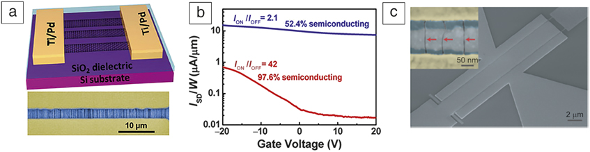
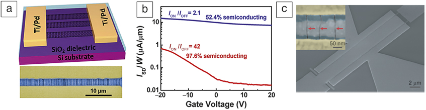
Depending on its rolling angle and radius, a SWCNT can be either metallic or semiconducting. A great advantage of CNTs over graphene is that semiconducting (s-) SWCNTs have tunable bandgaps due to quantum confinement. Therefore, s-SWCNTs have promising applications in both digital and analog electronics ( Figure 2a–c). Reference Che, Wang, Liu, Liu, Lin, Parker, Beasley, Wong and Zhou6,Reference Steiner, Engel, Lin, Wu, Jenkins, Farmer, Humes, Yoder, Seo, Green, Hersam, Krupke and Avouris7 Until recently, the gate length of s-SWCNT FETs has been scaled down to 5 nm, Reference Qiu, Zhang, Xiao, Yang, Zhong and Peng8 and they perform better than silicon counterparts at the same scale. Moreover, a p-channel s-SWCNT transistor footprint containing all components has been scaled down to 40 nm, Reference Cao, Tersoff, Farmer, Zhu and Han9 according to the International Technology Roadmap for Semiconductors. These results indicate that s-SWCNT transistors can actually be fabricated with dimensions and performance that make them a compelling replacement for Si FETs.
Applications of carbon nanotubes (CNTs) in nanoelectronics. (a) (top) Schematic and (bottom) a scanning electron microscope (SEM) image of a backgated CNT transistor. (b) Source-drain current (I SD) versus gate-source voltage (VGS) curves of backgate devices with 52.4% and 97.6% semiconducting CNTs. The ON/OFF current ratio (I ON/I OFF) for the transistor using 97.6% semiconducting CNTs is 42, much higher than the 2.1 for the transistor using 52.4% semiconducting CNTs. Note: W, width. Reproduced with permission from Reference Che, Wang, Liu, Liu, Lin, Parker, Beasley, Wong and ZhouReference 6. © 2012 American Chemical Society. (c) SEM image of a CNT radio-frequency transistor. (Inset) Magnified and colorized SEM image of the transistor channel showing three parallel CNTs (highlighted by red arrows) bridging the gated region (gray color) between source and drain electrodes (golden color). Reproduced with permission from Reference Steiner, Engel, Lin, Wu, Jenkins, Farmer, Humes, Yoder, Seo, Green, Hersam, Krupke and AvourisReference 7. © 2012 American Institute of Physics.
Nano-optoelectronics
CNTs and graphene have remarkable optical properties. Graphene has a featureless optical absorption spectrum over a wavelength range from 300 to 2500 nm, Reference Bae, Kim, Lee, Xu, Park, Zheng, Balakrishnan, Lei, Kim, Song, Kim, Kim, Ozyilmaz, Ahn, Hong and Iijima10 and a single layer of graphene absorbs 2.3% of the incident light with minimum reflection (<0.1%) over this same range. Reference Nair, Blake, Grigorenko, Novoselov, Booth, Stauber, Peres and Geim11 Other intriguing optical properties of graphene, including a high optical damage threshold and high third-order optical nonlinearity, Reference Lim, Chen, Clark, Goh, Ng, Tan, Friend, Ho and Chua12 and electroluminescence from pristine graphene, Reference Essig, Marquardt, Vijayaraghavan, Ganzhorn, Dehm, Hennrich, Ou, Green, Sciascia, Bonaccorso, Bohnen, von Loehneysen, Kappes, Ajayan, Hersam, Ferrari and Krupke13 have also been reported. CNTs also exhibit strong optical absorption and emission with energies determined by the CNT chirality, Reference Bachilo, Strano, Kittrell, Hauge, Smalley and Weisman14 large radiative (up to 100 ns) Reference Wang, Dukovic, Brus and Heinz15 and fluorescence lifetimes (up to 100 ps) Reference Huang, Pedrosa and Krauss16 at room temperature, photoluminescence, Reference O’Connell, Bachilo, Huffman, Moore, Strano, Haroz, Rialon, Boul, Noon, Kittrell, Ma, Hauge, Weisman and Smalley17 and electroluminescence. Reference Misewich, Martel, Avouris, Tsang, Heinze and Tersoff18
The excellent optical properties combined with the unique electrical properties enable CNTs and graphene to be used in novel nano-optoelectronics. An example is photodetectors, which convert light signals or optical power into electrical current and are a key component in optoelectronic devices. Different from conventional semiconductor photodetectors, graphene enables detectors to have a wide absorption range, from ultraviolet to infrared, and an ultrafast response due to the high mobilities of both electrons and holes. The application of s-SWCNTs to photodetectors has also been extensively studied based on their thermal and photo effects. Reference Yang, Wang, Zeng, Zhang and Peng19 These photodetectors have promising applications in remote sensing, night vision, reconnaissance, medical imaging, thermal imaging, and chemical detection. Interestingly, electroluminescence can be achieved in both ambipolar and unipolar CNT FETs, Reference Misewich, Martel, Avouris, Tsang, Heinze and Tersoff18,Reference Chen, Perebeinos, Freitag, Tsang, Fu, Liu and Avouris20 indicating the potential to produce solid-state light sources such as light-emitting diodes. The diameter-dependent CNT excitonic binding energy allows tunability of the photoresponse, showing promising photoluminescent applications. Reference O’Connell, Bachilo, Huffman, Moore, Strano, Haroz, Rialon, Boul, Noon, Kittrell, Ma, Hauge, Weisman and Smalley17 A graphene-based optical modulator with an operation frequency up to 1 GHz has been demonstrated. Reference Liu, Yin, Ulin-Avila, Geng, Zentgraf, Ju, Wang and Zhang21 In addition, CNTs and graphene are also attractive for use in mode-locked lasers, notch filters, and optical polarizers. However, many challenges remain. For example, because graphene does not have a bandgap, a photodetector would produce a sizable dark current, leading to heating and excessive shot and thermal noise. Since the emitted light power and fluorescence efficiency are rather low, there is currently limited scope for the use of CNTs in light-emitting applications.
Despite the many challenges facing CNTs and graphene for nanoelectronics and nano-optoelectronics, they are being addressed with rapidly developing nanotechnology. The unique electronic and optical properties of CNTs and graphene have motivated researchers to explore new device configurations (e.g., graphene-based bilayer pseudospin FETs and tunnel FETs). It may be possible to make interconnects from graphene and metallic SWCNTs, which would eventually allow the development of all-carbon integrated circuits (ICs) in which both the active devices and the interconnects are based on graphene and CNTs.
Flexible thin-film devices
Due to the stringent requirements for the quality of CNTs and graphene for nanoelectronic and optoelectronic devices, CVD-grown CNTs and graphene may first be used for flexible devices, replacing traditional rigid silicon, metal, and metal oxide materials, because CNTs and graphene can form thin films through interweaving of CNTs and the linking of the boundaries of graphene grains over a large area, at low cost. These films also have excellent properties, including high transparency and conductivity, good flexibility, and high stability, indicating their strong potential for use in future flexible and transparent electronic and optoelectronic devices, Reference Du, Pei, Ma and Cheng22–Reference Sun, Liu, Ren and Cheng24 which are built on flexible plastic substrates and are lightweight, thin, portable, and wearable.
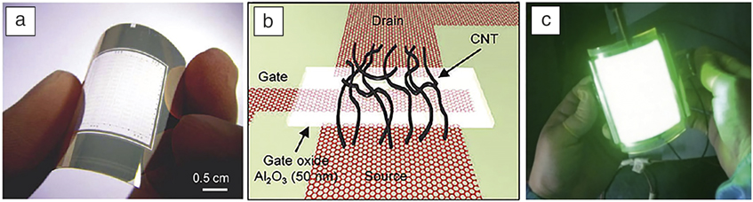
A thin-film transistor (TFT) is primarily used for driving circuits in the liquid-crystal displays of televisions, computer monitors, and mobile phones. CNT and graphene films are promising for the construction of flexible and transparent TFTs. They serve as semiconducting channels and transparent electrodes, but can also be used as interconnects in TFTs and ICs, and hence, make all-carbon film devices possible. Both all-CNT Reference Zou, Li, Liu, Jin, Qian, Jiang and Fan25 and all-graphene Reference Lee, Kim, Jang, Yoon, Lee, Hong, Rogers, Cho and Ahn26 TFTs have been demonstrated. However, due to the absence of a bandgap, TFTs with a graphene channel show a low ON/OFF current ratio, while a s-SWCNT film is a more suitable channel material. Both graphene and CNTs can meet the electrical and optical requirements of transparent conductive electrodes (TCEs). A CNT-graphene TFT with a graphene film as the electrode and an s-SWCNT film as the channel has shown good overall performance ( Figure 3a–b). Reference Yu, Lee, Chae, Perello, Han, Yun and Lee27 Based on CNT and graphene films, ICs, including combinational logic, sequential logic, and driving circuit for an active matrix organic light-emitting diode (OLED) display, have been demonstrated. Reference Che, Chen, Gui, Liu, Liu and Zhou28
Applications of carbon nanotubes (CNTs) and graphene in flexible thin-film devices. (a) Photo of a transparent graphene-CNT integrated-circuit array and (b) schematic of a thin-film transistor using graphene electrodes and a single-wall CNT network channel on a flexible transparent poly(ethylene terephthalate) substrate. Reproduced with permission from Reference Yu, Lee, Chae, Perello, Han, Yun and LeeReference 27. © 2011 American Chemical Society. (c) Photo of an 80 × 70 mm2 monolithic flexible organic light-emitting diode using a graphene transparent conductive electrode. Reference Zhang, Du, Zhang, Sun, Yin, Ma, Chen, Ma, Cheng and Ren29
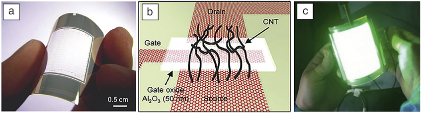
It is worth noting that as TCEs with excellent flexibility, CNT and graphene films are promising for use in newly emerging flexible optoelectronic devices, such as touch panels, OLEDs, and organic photovoltaic (OPV) cells. High-performance CNT- and graphene-based OPV cells and OLEDs with different device structures have been widely investigated. Reference Du, Pei, Ma and Cheng22 Recently, we produced an 80 × 70 mm2 monolithic flexible graphene-based OLED (Figure 3c) with a high brightness of ∼10,000 cd m–2 that can satisfy the requirements for lighting sources and displays. Reference Zhang, Du, Zhang, Sun, Yin, Ma, Chen, Ma, Cheng and Ren29 Due to the strict requirements for the surface roughness, work function, and hydrophilicity of TCEs, much work needs to be done for the practical use of CNT- and graphene-TCEs in OLEDs and OPV cells. However, CNT and graphene TCEs have already been commercially used in touch panels and integrated into smartphones.
Energy storage based on CVD-grown CNTs and graphene
Lithium battery
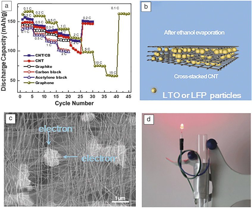
Lithium (Li)-ion batteries (LIBs) are highly attractive rechargeable batteries because of their high capacity. Most cathode materials (e.g., LiFePO4 [LFP], LiCoO2) used in these batteries face problems of low electrical conductivity and limited ion transport. Therefore, conductive additives are necessary to improve these properties. Commercial conductive additives include carbon black (CB), Reference Dominko, Gaberscek, Drofenik, Bele, Pejovnik and Jamnik30–Reference Liu, Zheng, Simens, Minor, Song and Battaglia32 graphite, Reference Shin, Cho and Jang33 CNTs, Reference Liu, Peng, Zhang, Huang, Liu, Wang, He, Zhu and Wei34 carbon nanofibers, Reference Thorat, Mathur, Harb and Wheeler35 and graphene nanosheets (GNs). Reference Su, He, Li, Chen, You, Wei, Lv, Yang and Kang36 The capacity retention and rate performance of electrodes with different conductive carbon additives are shown in Figure 4a. Reference Shin, Cho and Jang33,Reference Liu, Peng, Zhang, Huang, Liu, Wang, He, Zhu and Wei34,Reference Yang, Wang, Tang, Wang, Li, Hu, Li, Liang, Sham and Sun37 Those with CNT or graphene additives show better electrochemical performance.
Performance and structure of composite electrode materials for lithium-ion batteries. (a) Rate performance of a LiFePO4 (LFP)/C cathode, showing the high efficiency of LFP/carbon nanotube (CNT)/carbon black (CB) or LFP/graphene nanosheet composite cathodes. Data for graphite, CB, and acetylene black are from Reference Shin, Cho and JangReference 33; data for CNTs and CNT/CB are from Reference Liu, Peng, Zhang, Huang, Liu, Wang, He, Zhu and WeiReference 34; data for graphene nanosheets is from Reference Yang, Wang, Tang, Wang, Li, Hu, Li, Liang, Sham and SunReference 37. Note: 1 C = 170 mA/g in Reference Liu, Peng, Zhang, Huang, Liu, Wang, He, Zhu and WeiReferences 34 and Reference Yang, Wang, Tang, Wang, Li, Hu, Li, Liang, Sham and Sun37, and 150 mA/g in Reference Shin, Cho and JangReference 33. Reproduced with permission from Reference Shin, Cho and JangReference 33, Reference Liu, Peng, Zhang, Huang, Liu, Wang, He, Zhu and Wei34, and Reference Yang, Wang, Tang, Wang, Li, Hu, Li, Liang, Sham and Sun37. © 2006 Elsevier. © 2013 American Chemical Society, and © 2013 The Royal Society of Chemistry. (b) Schematic and (c) scanning electron microscope (SEM) image of a LFP (white particles)-confined CNT thin-film electrode, and (d) photo of the corresponding flexible battery. Reproduced with permission from Reference Wu, Wu, Luo, Wang, Zhao, Wei, Liu, Jiang, Wang and FanReference 43. © 2014 Royal Society of Chemistry. Note: LTO, Li4Ti5O12.
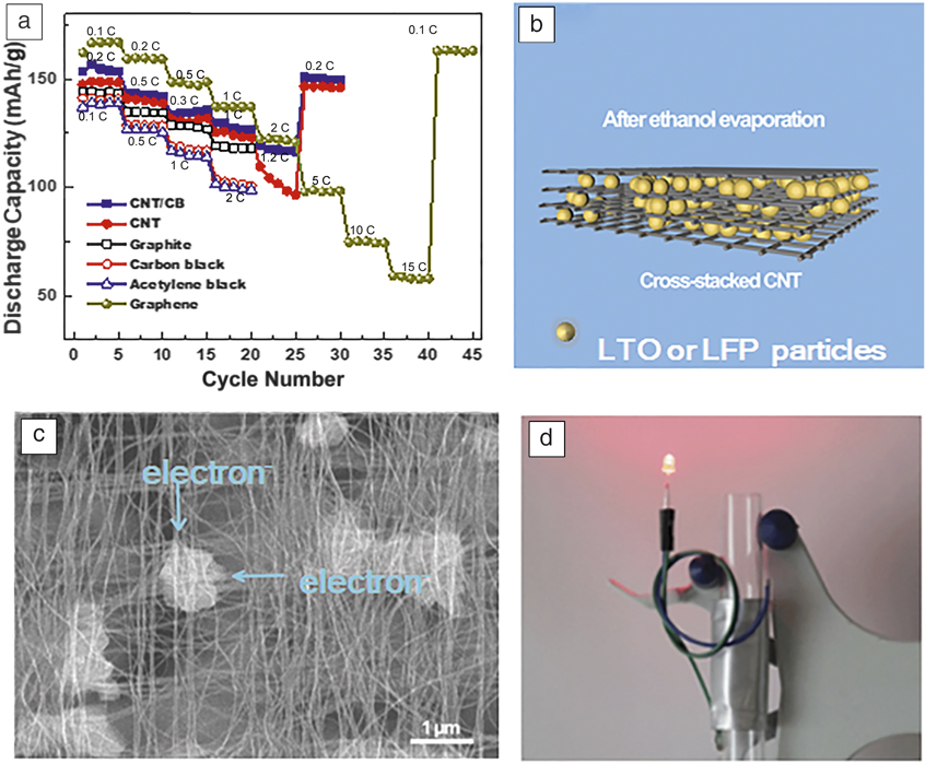
CNTs with increased electrical connectivity and mechanical integrity may produce a “point-to-line” contact mode (point refers to active material particle, such as LFP, while line refers to CNT), which forms a long-range conductive network and therefore enhances the rate capability and cycle life of LIBs. Reference De Volder, Tawfick, Baughman and Hart38 A 2D GN with a planar and flexible contact area can link active materials following a unique “plane-to-point” mode (plane refers to GN) and construct an effective electron transfer network. However, the planar structure of the graphene sheets blocks fast Li+ ion transport, and a steric effect resulting from heavy polarization occurs at a relatively high charge/discharge rate (>3 C), Reference Su, He, Li, Chen, You, Wei, Lv, Yang and Kang36 which limits its use in high-power batteries. Because of cost considerations, CNTs are currently the most widely used additive in LIBs. In addition, hybridized additives of CNTs and CB have demonstrated high efficiency in building composite cathodes with excellent Li storage performance and good economical efficiency. Reference Liu, Peng, Zhang, Huang, Liu, Wang, He, Zhu and Wei34 The hybridized point-to-point and line-to-point contacts of CBs, CNTs, and active material particles produce efficient electron transport. Therefore, a major commercial success of CNTs is their use as an additive in LIBs. At the present time, CNT conductive additives used in LIBs for electric vehicles and smartphones represent the largest use of CNTs in China, Reference Jia and Wei1 although diameter uniformity, number of walls, length, purity, and dispersability need to be further optimized.
Flexible and stretchable energy storage
Electronic devices that are flexible have been quickly developed in recent years. Reference Liu, Song, Kong and Cui39 As a consequence, the development of flexible electrochemical energy-storage devices is extremely important. CVD-grown CNTs and graphene have great potential for these applications. More importantly, CNTs and graphene have significantly better mechanical properties than other active materials, and therefore, have obvious advantages for bendable electrodes. First, they can be bent to an extremely small radius of curvature of ∼20 nm. Reference Falvo, Clary, Taylor, Chi, Brooks, Washburn and Superfine40 Second, strong interactions between CNT bundles and graphene sheets can maintain integrity during repeated bending. Third, CNTs and graphene can be easily assembled into films or foams by various wet or dry processes.
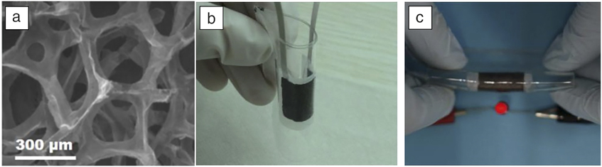
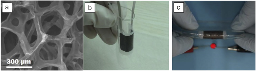
There are three methods of using CNTs and graphene for flexible electrodes. Reference Wen, Li and Cheng41 (1) They can act as a conductive phase to improve the conductivity of nonconductive substrates. Cui et al. created a highly conductive CNT paper by conformally coating CNTs onto commercial paper, which was then used as flexible current collectors and electrodes. Reference Hu, Choi, Yang, Jeong, La Mantia, Cui and Cui42 (2) They can serve as a flexible current collector or freestanding matrix for hosting active materials. Fan et al. fabricated CNT current collectors by cross-tacking continuous CNT films drawn from super-aligned CNT arrays loaded with LFP/LTO (Li4Ti5O12), layer by layer (Figure 4b–d). Reference Wu, Wu, Luo, Wang, Zhao, Wei, Liu, Jiang, Wang and Fan43 The electrodes demonstrated excellent reversibility, high flexibility, and light polarization in both flat and bent conditions. Reference Wang, Luo, Wu, He, Zhao, Wang, Jiang and Fan44 (3) CNT or graphene composites can be used as freestanding composite flexible electrodes. We have reported a thin, lightweight, and flexible LIB designed from CVD-graphene foam. The three-dimensional (3D), flexible, and conductive interconnected graphene network, as both a highly conductive path for electrons and lithium ions and a lightweight current collector, was loaded with LTO as the anode and LFP as the cathode, respectively ( Figure 5a–c). Reference Li, Chen, Ren, Li and Cheng45 This battery has shown good flexibility, high capacity, high rate (up to 200 C), and long life cyclic performance (over 100 cycles at a high rate of 10 C with only 4% capacity loss) even under repeated bending to a radius as small as 5 mm. Therefore, both CNTs and graphene grown by CVD play a significant role in constructing bendable, stretchable, and compressible energy-storage devices. However, CNTs appear to be more promising, considering the high cost and limited amount of graphene that can be produced by CVD.
Demonstration of a thin, lightweight, and flexible Li4Ti5O12 (LTO)/graphene foam (GF)//LiFePO4/GF full battery. (a) Scanning electron microscope image of flexible GF loaded with LTO. (b) Photo of the bent battery encapsulated by poly(dimethylsiloxane), showing its good flexibility. (c) The bent battery lighting a red light-emitting diode device. Reproduced with permission from Reference Li, Chen, Ren, Li and ChengReference 45. © 2012 National Academy of Sciences.
Composites based on CVD-grown CNTs and graphene
Integration of CNTs or graphene in various matrices, including metals, ceramics, and polymers to form advanced composites is one of the most promising routes for taking full advantage of their unique structure and properties for use with dramatically improved properties at a low loading. Reference Sun, Sun, Li and Peng46–Reference Du, Bai and Cheng48 However, CVD-grown CNTs and graphene are different in many respects for inclusion in composites. In general, CVD-grown graphene is not freestanding, but is supported on a metal catalyst foil. Thus, it is difficult to use it directly as a filler in a matrix. On the other hand, porous graphene scaffolds with a 3D network structure can be synthesized by CVD. Reference Chen, Ren, Gao, Liu, Pei and Cheng49 Using this scaffold, flexible graphene/poly(dimethylsiloxane) composite films with a low density of ∼0.06 g cm–3 and electromagnetic interference shielding effectiveness up to 500 dB • cm3/g have been reported, which is about one order of magnitude higher than those of typical metals and carbon/polymer composites. Reference Chen, Xu, Ma, Ren and Cheng50
CVD-grown CNTs can have various forms—powder, film, array, paper, sponge, and fiber. As a result, they can be used as both fillers and scaffolds to construct composites. By using CNT fillers, both randomly oriented and aligned CNT-based composites can be obtained. The strength and elastic modulus of randomly oriented CNT-based composites are generally much lower than those of aligned CNT-based composites along their alignment direction. CNT-based composites retain the CNT structure, thus making better use of the CNT properties. Another important characteristic of CNTs is that they can be spun into fibers by directly spinning from a composite solution/melt or by dry spinning and then integrating with matrix materials.
The mechanical properties of CNT-based composites combined with electrical, thermal, and other properties have been extensively investigated. This is especially the case for CNT/polymer composites, since polymers can be easily processed and fabricated into intricately shaped components using conventional methods with a low manufacturing cost. For example, SWCNT/polyvinyl alcohol composite fibers with a high CNT percentage of 60 wt% have been fabricated by a modified coagulation spinning process. These composite fibers have a maximum tensile strength of 1.8 GPa, comparable to that of spider silk. Reference Dalton, Collins, Munoz, Razal, Ebron, Ferraris, Coleman, Kim and Baughman51 Due to the high-aspect ratio and conductivity, an aligned SWCNT/epoxy composite with a low percolation threshold of 0.0025 wt% was obtained. Reference Sandler, Kirk, Kinloch, Shaffer and Windle52 The conductivity can easily reach 350 S cm–1 for a highly aligned CNT/poly(acrylic acid) composite at room temperature. Reference Guo, Liu, Sun, Yang, Kia and Peng53 In addition, CNTs can improve the thermal-transport properties of polymer composites. Reference Huang, Liu, Wu and Fan54
CNT-based composites are also used as structural materials in many fields such as woven fabrics and textiles, aerospace, sports, infrastructure, and defense. Some sporting goods, including tennis racquets, baseball bats, and bicycle frames with CNT-based composites have been commercialized. NASA scientists have even considered space elevators using a super-strong CNT/polymer composite fiber as the cable. Taking advantage of their many properties, including high electrical and thermal conductivity, high thermal stability, and nonlinear optical properties, CNT- and graphene-based composites can be exploited as electromagnetic interference (EMI) shielding packages; electromagnetic absorption materials for stealth applications; wafer carriers (a container for transporting or holding wafers) for the microelectronics industry; coatings for enclosures, antistatic materials, lightning strike protection, deicing, and structural health monitoring for aircrafts; thermal interface materials for electronic components; flame retardants; and anticorrosion layers for metals. Most of these applications are being pursued industrially by many companies. However, in many respects, the reinforcing effects are far from what are expected. Technical barriers, such as structure control of the CNT and graphene fillers and scaffolds, dispersion of graphene and CNT fillers in matrices, interfacial interactions between graphene and CNTs with matrices, and contact between individual graphene sheets and CNTs need to be tackled.
Other applications of CVD-grown CNTs and graphene
Sensors
The use of SWCNTs and graphene as components in sensors is motivated by their remarkably high surface-to-volume ratio and the ability of each surface atom to contribute to the sensing response. Electrical impedance is in response to the surrounding environment, which is typically modulated by the adsorption of target molecules on the exposed surface. Changes can be electrically evaluated in resistor, transistor, or capacitor structures. Low detection limits and high selectivity require engineering the CNT/graphene surface and appropriate sensor design. Reference De Volder, Tawfick, Baughman and Hart38 SWCNT gas sensors respond to the surface coverage of analytes, unlike conventional gas sensors, which respond to their concentration. Reference Snow, Perkins, Houser, Badescu and Reinecke55 As a result, they can offer high detection limits (ppb) for low-vapor-pressure analytes, such as chemical warfare agents and explosives, which cannot be detected by conventional gas sensors. Reference Cao and Rogers56 Since the diameters and carrier densities of SWCNTs are comparable to the sizes and surface-charge densities of biomacromolecules, SWCNTs can serve as ultrasensitive transducers in biosensors. Reference Kim, Rusling and Papadimitrakopoulos57 Products under development include inkjet-printed test strips for estrogen and progesterone detection, microarrays for DNA and protein detection, sensors for NO2 and cardiac troponin (a type of protein), and toxin detection in the food industry, military, and environmental applications. Reference De Volder, Tawfick, Baughman and Hart38 Since each carbon atom of graphene can potentially contribute to the sensing response, graphene’s electrical conductivity is incredibly sensitive to the adsorption of chemical species on its surface. This sensitivity, together with its extremely low intrinsic noise, allows such sensors to be capable of a wide sensitivity range, from the single-molecule level to high concentrations. Reference Hammock, Chortos, Tee, Tok and Bao58 However, CVD-graphene-based sensors are still in the incubation stage, and many challenges such as repeatability, selectivity, and cost need to be overcome.
Catalysis
Heteroatom-doped CNTs and graphene, as well as their composites, can be engineered into efficient catalysts for the oxygen-reduction reaction (ORR). N-doped vertically aligned CNT (VACNT) arrays show a much higher catalytic activity, lower overpotential, smaller crossover sensitivity, and better long-term operation stability than commercial Pt/C catalysts in alkaline media. Reference Gong, Du, Xia, Durstock and Dai59 Dai et al. first synthesized N-doped graphene films by the CVD of methane in the presence of ammonia, Reference Qu, Liu, Baek and Dai60 and found that the steady-state catalytic current, the long-term stability, tolerance to crossover, and poisoning effect are better, while the onset potential and half-wave potential are not much lower than those of Pt/C for oxygen reduction in an alkaline electrolyte. Lou et al. post-doped 3D graphene foam with graphitic C3N4 at an elevated temperature, and the resulting N-doped foam demonstrated a similar onset potential to a Pt catalyst in an alkaline medium and high activity, longtime stability, and superior crossover resistance. Reference Wu, Ma, Yadav, Yang, Zhang, Vajtai, Lou and Ajayan61
CNTs and graphene can also be used as supports for high-activity noble-metal (Pt, Pt-based alloy, and Ag) catalysts and boost their ORR activity since they are able to buffer the agglomeration of catalyst nanoparticles and improve electronic conductivity. It has been reported that the use of CNTs as a support for Pt can potentially reduce Pt usage by 60% compared to CB. Reference Matsumoto, Komatsu, Arai, Yamazaki, Kijima, Shimizu, Takasawa and Nakamura62 A core–shell structure (i.e., an active heteroatom-doped carbon shell closely wrapped around a core of CNTs), may enable the production of fuel cells that do not require Pt. Reference Yasuda, Furuya, Uchibori, Kim and Murakoshi63
Water purification
CVD-grown graphene and CNTs have been extensively studied for their extraordinary water-transport and sieving properties. Single-layer graphene offers the thinnest 2D membrane with the lowest possible hydrodynamic resistance. Reference Celebi, Buchheim, Wyss, Droudian, Gasser, Shorubalko, Kye, Lee and Park64 By creating subnanometer pores in the graphene layer, a nanoporous graphene membrane demonstrated selective ionic transport for nanofiltration and the potential for desalination. Reference Celebi, Buchheim, Wyss, Droudian, Gasser, Shorubalko, Kye, Lee and Park64,Reference O’Hern, Jang, Bose, Idrobo, Song, Laoui, Kong and Karnik65 However, the limited volume and high cost of CVD-grown graphene as well as the repeatability of creating nanopores, remain great obstacles for their practical applications.
CNTs have the following three unique properties that are relevant for membrane-based separation. (1) The CNT hollow cores, ranging from ∼1 to 50 nm diameter, are ideal pore sizes in nanofiltration and ultrafiltration. Reference Goh, Karahan, Wei, Bae, Fane, Wang and Chen66 (2) The atomically smooth, hydrophobic graphitic inner channels of CNTs provide low-friction transport of water. Reference Noy, Park, Fornasiero, Holt, Grigoropoulos and Bakajin67 (3) The functionalization of a hollow core surface can engineer membrane-sieving capabilities. Therefore, studies of as-grown/functionalized CNTs in water decontamination with respect to heavy metals, fluorides, arsenic compounds, and toxic organics have been reported, and VACNT arrays show greater advantages than other forms of CNTs. Reference De Volder, Tawfick, Baughman and Hart38
The VACNT membranes can be categorized into two types: (1) dense-array outer-wall CNT membranes that use the interstices between nanotubes in a vertical array of CNTs; and (2) open-ended CNT array membranes that use the CNT hollow cores by opening the tips and filling the interstices between the CNTs with a suitable filler. It has been reported that the water purification capacity of VACNT membranes is almost two orders of magnitude greater than that attainable using traditional polymer membranes. The antibiofouling capability of CNT wall membranes is considerably enhanced by their ability to impede bacterial adhesion, in addition to their ability to resist biofilm formation. Reference Lee, Baek, Lee, Jeong, Lee, Yoon and Kim68 Though CNT-based membranes have shown tremendous promise in desalination and water purification applications, the high cost and the scale-up growth of VACNTs are challenges for large-scale applications.
Summary and perspectives
CVD-grown graphene shows great promise for applications in electronics, flexible energy storage, EMI shielding, and sensors. In particular, graphene might be the best flexible transparent conductor known, and it may surpass SWCNTs due to its low roughness and inherently metallic nature. Therefore, CVD-graphene may find commercial applications in flexible optoelectronic devices, such as touch panels, OLEDs, and OPV cells. However, their commercial applications are still at an early stage, waiting for breakthroughs in low-cost, large-scale, controllable synthesis methods and easy, clean transfer techniques.
CVD-grown CNT powder has been used in many products, including LIBs, composites, and water filters. The development of cost-effective, environmentally friendly, and reliable processes for controlled CNT production, depending on the intended use, is still highly desired. VACNTs demonstrate great promise in supercapacitors, water purification, catalysts, and more, and bridge the gap between the nanoscale properties of CNTs and the length scales of bulk engineering materials. However, the quality of VACNTs still needs to be improved.
SWCNT commercialization in electronics such as transistors and transparent conductive films is starting to show significant progress. High-end products in electronics, optoelectronics, and solar cells are greatly anticipated for SWCNTs because of their superior properties. SWCNTs offer great advantages in semiconducting applications because of their bandgap. The applications of CVD-grown SWCNTs are starting to emerge, but are dependent on the progress of low-cost, high purity, uniform electrical types, or even single-chirality SWCNT synthesis techniques.
Acknowledgments
This work was supported by the Ministry of Science and Technology of China (Grant 2016YFA0200101), and the National Natural Science Foundation of China (Grants 51625203, 51532008, 51521091, 51572265, and 51572264). The research leading to these results has received funding from the European Union Seventh Framework Programme (FP7/2007-2013) under Grant Agreement No. 604472 (IRENA project), the Aalto Energy Efficiency Research Program through the MOPPI Project, and by the Academy of Finland via Project Nos. 286546 and 292600.

Peng-Xiang Hou is a professor in materials science and engineering at the Institute of Metal Research, Chinese Academy of Sciences (IMR-CAS). She received her BSc degree in 1999 and PhD degree in 2003, both in materials science from IMR-CAS. Her research focuses on carbon nanotube-controlled synthesis, properties, and their applications. Hou can be reached by phone at +86 24 8397 0720 or email at pxhou@imr.ac.cn.

Jinhong Du is a research professor at the Institute of Metal Research, Chinese Academy of Sciences (IMR-CAS). She received her PhD degree in materials science at IMR-CAS in 2003. Her research focuses on the preparation, properties, and applications of nanostructured materials (carbon nanotubes and graphene)-based films and composites. Du can be reached by phone at +86 24 8397 0720 or email at jhdu@imr.ac.cn.

Chang Liu is a professor at the Institute of Metal Research, Chinese Academy of Sciences (IMR-CAS). He received his PhD degree in materials science in 2000 at IMR. He is the leader of the group studying the synthesis, properties, and applications of CNTs. Liu can be reached by phone at +86 24 8397 8280 or email at cliu@imr.ac.cn.

Wencai Ren is a professor of materials science at the Institute of Metal Research, Chinese Academy of Sciences (IMR-CAS). His research interests focus on the synthesis of graphene and other two-dimensional materials and their applications in energy storage, composites, and optoelectronics. He has published more than 100 papers, including in Nature Materials, Nature Nanotechnology, Nature Communications, Proceedings of the National Academy of Sciences U.S.A., Advanced Materials, and Journal of the American Chemical Society, and holds more than 30 patents. Ren can be reached by phone at +86 24 2397 1472 or email at wcren@imr.ac.cn.

Esko I. Kauppinen is the Vice Dean of research, innovations, and industry relationships and is a tenured professor of physics in the Department of Applied Physics in the School of Science at Aalto University, Finland. He has published more than 380 papers. His research focuses on single-wall carbon nanotube synthesis, characterization, and thin-film applications as well as in the gas-phase synthesis of particles for inhalation drug delivery. Kauppinen can be reached by phone at +358 4 0509 8064 or email at esko.kauppinen@hut.fi.

Hui-Ming Cheng is professor and director of the Advanced Carbon Research Division at Shenyang National Laboratory for Materials Science, Institute of Metal Research, Chinese Academy of Sciences, and the Low-Dimensional Material and Device Laboratory at the Tsinghua-Berkeley Shenzhen Institute, Tsinghua University, China. His research focuses on the synthesis and applications of carbon nanotubes, graphene, other low-dimensional materials, energy-storage materials, photocatalytic semiconducting materials, and bulk carbon materials. Cheng can be reached by phone at +86-24-2397 1788 or by email at cheng@imr.ac.cn or hmcheng@sz.tsinghua.edu.cn.