Introduction
As frequency applications advance beyond 110 GHz, particularly in the D-band [110–170 GHz] and the recently released IEEE 805.15.3d band [252–425.52 GHz] [1], transistors capable of operating in the terahertz range are essential for circuits like power amplifiers (PA) and low-noise amplifiers (LNA), which are critical in mm-wave and sub-mm-wave radio front-ends. Field-effect transistors (FETs) are particularly significant due to their ability to achieve extremely high cut-off frequencies. One of the leading technologies for millimeter-wave and terahertz use is the indium phosphide (InP)-based high-electron mobility transistor (HEMT), which has demonstrated cut-off frequencies exceeding 1 THz. Prominent organizations such as Northrop Grumman and the Fraunhofer Institute for Applied Solid State Physics IAF have successfully developed terahertz integrated circuits using transistors capable of oscillating beyond 1 THz. When developing stand-alone transistors, direct measurements can be performed up to the cut-off frequency to accurately determine the maximum oscillation frequency (f max). However, such measurements remain challenging, with most fT and fmax assessments relying on extrapolation from measurements below 110 GHz. To the authors’ knowledge, no study has yet investigated the measurement of a single transistor across the entire frequency range up to 1.1 THz.
We propose an on-wafer measurement procedure for one and the same device over a large frequency band from 250 MHz to 1.1 THz. In order to effectively perform this measurement, it is necessary to optimize the transistor’s coplanar accesses for high-frequency measurement and implement them as calibration standards for an on-wafer multiline Thru-Reflect-Line (mTRL) calibration kit. Previous work [Reference Younes, Wichmann, Lepilliet, Ducournau and Bollaert2] by the author focused on the optimization of the coplanar waveguide and the on-wafer characterization of passive components. An earlier version of this paper was presented at the European Microwave Conference in 2024 and was published in its Proceedings [Reference Younes, Samnouni, Lepilliet, Wichmann, Ducournau and Bollaert3]. In this work, we provide further explanation of the optimizations performed on the coplanar lines, including an analysis of the characteristic impedance ZC and the Poynting vector distribution to support the design choices. We also present further details on the design and fabrication of the calibration kit, including a study on the influence of the thru line length in the multiline TRL (mTRL) calibration. This analysis justifies the choice of an 80-μm-long thru line used in the kit. As was reported in [Reference Younes, Samnouni, Lepilliet, Wichmann, Ducournau and Bollaert3], we fabricated an 80-nm InAlAs/InGaAs/InAs InP-HEMT using the optimized transistor coplanar accesses, the epitaxial structure and process of fabrication can be found in [Reference Samnouni, Wichmann, Wallart, Coinon, Lepilliet and Bollaert4]. In this work, we will provide the results of transistors with different gate widths WG = 2 × 4 μm, WG = 2 × 8 μm, and WG = 2 × 12 μm.
Optimization of the coplanar accesses
The coplanar waveguide (CPW) configuration facilitates the propagation of a quasi-TEM mode [Reference Riaziat, Majidi-Ahy and Feng5]. At very low frequencies, the structure of the electromagnetic field mimics that of a transverse electromagnetic (TEM) mode. However, as the frequency increases, higher order propagation modes, also called surface wave modes, may be excited [Reference Spirito, Arz, Phung, Schmückle, Heinrich and Lozar6]. This poses a significant challenge in CPW design due to the emergence of multiple propagation modes. If these undesired modes are not prevented, the coplanar waveguide may incur high losses. In such cases, the Poynting vector points toward the substrate showing that the electromagnetic energy will leak into the substrate [Reference Zhang7]. The different characteristics of the coplanar waveguide such as the effective dielectric constant and the attenuation have been previously studied by Ponchak [Reference Ponchak, Tentzeris and Katehi8]. In order to verify the behavior of the CPW over a large frequency band, we started by simulating using Ansys’ HFSS [9], the standard coplanar waveguide configuration used to measure the previously reported transistors up to 110 GHz [Reference Samnouni, Wichmann, Wallart, Coinon, Lepilliet and Bollaert4]. The configuration of the CPW is presented in the subfigure of Fig. 1. W is the signal conductor width, G the gap between signal conductor and ground plane, d the ground-to-ground distance calculated using d = W + 2 G and L the length of CPW.
Simulated S-parameters and ZC of a standard CPW configuration from 250 MHz to 1.1 THz and configuration of the CPW.

From the S-parameter simulations presented in Fig. 1, we notice that this topology experiences a significant drop in the transmission coefficient (S 12 and S 21), with values reaching −17 dB at a frequency of 1.1 THz. In fact, the transmission coefficient starts degrading largely beyond 200 GHz. Correspondingly, the reflection parameters S 11 and S 22 also start increasing at a frequency of 200 GHz, and beyond 500 GHz, the reflection parameters are nearly 0 dB. This indicates that at high frequencies, the topology presents a complete reflection of the signal along the transmission line. In addition, since we will be using the optimized coplanar accesses as mTRL calibration standards, it is crucial to verify that the characteristic impedance ZC of the coplanar waveguide maintains a 50 Ω value across the frequency band. Therefore, we calculate the characteristic impedance ZC of the CPW from the simulated S-parameters using the formula [Reference Galatro and Spirito10]:
 \begin{equation}{Z_C} = \,{Z_0}\sqrt {\frac{{{{\left( {1 + {S_{11}}} \right)}^2} - {S_{21}}^2}}{{{{\left( {1 - {S_{11}}} \right)}^2} - {S_{21}}^2}}} \end{equation}
Figure 1 also presents the calculated ZC. At low frequencies, we obtain a stable 50 Ω characteristic impedance. As the frequency increases beyond 200 GHz, the characteristic impedance deviates from the standard 50 Ω and increases to approximately 800 Ω at 1.1 THz. This suggests the emergence of undesired modes of propagations that enable the leakage of the electric field into the substrate. To further investigate this phenomenon, we monitored the Poynting vector of the excited signal at two distinct frequencies (Fig. 2). At 92 GHz, where S 21 is close to 0 dB and ZC is around 50 Ω, the Poynting vector shows that the transmission occurs inside the waveguide as expected. On the other hand, at 1000 GHz, where S 21 is around −14.6 dB and ZC equals 657 Ω, the Poynting vector shows that the electromagnetic energy is predominantly lost in the substrate. Therefore, we conclude that this standard CPW structure is not optimized for measurement up to 1.1 THz.
Poynting vector at 92 GHz (left) and 1000 GHz (right).

To optimize the coplanar waveguide, we simulated coplanar lines of length 100 µm, over the frequency band [250 MHz–1.1 THz], varying the ground-to-ground spacing. The distance is progressively reduced from the standard coplanar line value of 70–11.5 µm. Table 1 presents the different parameters used to obtain the ground-to-ground distances presented in the simulations. We calculated each of these parameters using TX-Line [11] to ensure a 50 Ω analytical characteristic impedance.
Simulated CPW design parameters

Figure 3 presents the simulated transmission parameter S 21 of the coplanar waveguide with different ground-to-ground spacings. We notice that the decrease of the ground-to-ground distance progressively improves the transmission coefficient over the whole frequency band. For a ground-to-ground distance of 70 µm, S 21 is −17 dB at 1.1 THz, while for a ground-to-ground spacing of 11.5 µm, S 21 increases to a value of −1.1 dB at 1.1 THz. Figure 3 also shows the equivalent simulated characteristic impedance calculated using equation (1) for the different ground-to-ground distances. Notably, the ground-to-ground distance of 11.5 µm maintains a characteristic impedance close to 50 Ω, indicating optimal impedance matching across the frequency band. In contrast, a ground-to-ground distance of 70 µm results in a characteristic impedance ZC of 717 Ω at 1.1 THz. Figure 4 displays the simulated S-parameters and the Poynting vector at 1000 GHz of a CPW with a ground-to-ground distance of 11.5 µm, it can be seen that the propagation direction remains concentrated around the signal conductor of the CPW instead of dispersing in the substrate. Therefore, the optimal ground-to-ground spacing for transistor measurement up to 1.1 THz is 11.5 µm. As indicated earlier, the S 21 and S 12 parameters present a value of −1.1 dB at 1.1 THz while the S 11 and S 22 parameters always have a value that does not exceed −23 dB.
Simulated transmission parameter S 21 and characteristic impedance ZC for different variations of the ground-to-ground spacing for a line of 100-µm length.

Simulated S-parameters of a CPW with a ground-to-ground distance = 11.5 µm from 250 MHz to 1.1 THz and Poynting vector (@ 1000 GHz).

However, the configuration of the probes used to measure the devices up to 1.1 THz limits the signal conductor width that can be electrically coupled to the structure to a value of 15.5 µm. To accommodate this, we added contact pads to the overall structure in order to correctly position the probes during on-wafer measurements. The subfigure of Fig. 5 shows the final design of the coplanar accesses consisting of a conventional coplanar line with a ground-to-ground distance of 11.5 µm with an added coplanar access having a ground-to-ground spacing of 36.5 µm as contact pads. Moreover, in order to measure the same component across all the frequency bands, we cannot reduce the width of the ground plane beyond 89.5 µm. This width is dictated by the larger 100-µm pitch of the probes, which is the distance between the signal conductor and each of the ground planes of the probes. Figure 5 represents the reflection and transmission parameters of the structure. We notice that the resulting S-parameters are close to a conventional coplanar waveguide having a ground-to-ground spacing of 36.5 µm. The contact pads largely impact the transmission in the structure and its characteristic impedance starting of 500 GHz.
Comparison between the simulated reflection S 11 and transmission S 21 parameters of the final topology shown in the subfigure (red) and a conventional coplanar waveguide having a ground-to-ground distance of 36.5 µm (green) from 250 MHz to 1.1 THz.

To mitigate the effects of the added pads, we implement an on-wafer multiline Thru-Reflect-Line (mTRL) calibration. This method shifts the reference plane from the extremities of the coplanar line, where the ground-to-ground distance equals 36.5 µm, closer to where the ground-to-ground distance equals 11.5 µm. Combining this topology with an on-wafer mTRL allows us to control the characteristic impedance of the resulting measurements, maintaining it at a 50 Ω value across the entire frequency band, as is set by the 11.5-µm coplanar line. In the next section, we conducted further studies on the different calibration techniques in particular the mTRL.
On-wafer multiline Thru-Reflect-Line calibration (MTRL)
Measurement calibration is an essential step in component characterization to minimize environmental errors that can cause inaccurate measurements. In many cases, an off-wafer calibration is done prior to device’s characterization. For the frequency ranges [250 MHz–110 GHz], [140–220 GHz] and [220–325 GHz], we usually apply the off-wafer Line-Reflect-Reflect-Match (LRRM) calibration method using the alumina impedance standard substrate (ISS) calibration kit provided by the probe manufacturer [12] matched with either a 100- or 50-µm pitch waveguide infinity probe [13]. Above 325 GHz, the off-wafer multiline Thru-Reflect-Line calibration technique, using a high resistivity silicon substrate [14], is paired with the formfactor provided T-wave probe (25-µm pitch) [15]. Consequently, in order to measure the indium phosphide high-electron mobility transistor over the large frequency band 250 MHz–1.1 THz, we developed a unique and accurate on-wafer calibration method in order to minimize the errors brought by calibrating with impedance standard substrates presenting different values of dielectric permittivity.
The choice of calibration method is influenced by minimizing manufacturing challenges. The mTRL was originally introduced by Marks in 1991 [Reference Marks16] then a more detailed version of the algorithm was published in 2002 [Reference DeGroot, Jargon and Marks17]. Unlike other methods such as LRRM or SOLT, the mTRL calibration method employs transmission lines as calibration standards without requiring a “match” standard (50-Ω load). This simplifies the fabrication of the calibration standards for large band measurement. The mTRL also modifies the reference plane of the measurements to the middle of the Thru line so that the losses of the added pads will be absorbed by the calibration’s error set. As reported in [Reference Younes, Samnouni, Lepilliet, Wichmann, Ducournau and Bollaert3], we fabricated an on-wafer mTRL calibration kit using the previously optimized coplanar accesses as calibration standards on InP substrate. The Reflect standard implemented is an open coplanar line. We use a combination of two or more Line standards to enhance the accuracy of the calibration. Each Line standard is a CPW similar in design to the Thru standard but differing in overall length by a value of ΔL. This difference in length introduces the necessary phase shift for accurate calibration across the frequency band. Each of the Line standards is designed to achieve a phase variation between 20° and 160° across the frequency range. This phase shift ensures accurate calibration by providing sufficient variation between the different Line standards, which is critical for properly characterizing the device under test.
A variation was also performed on the length of the Thru standard to select the optimal overall length and achieve the closest measurement match to the HFSS simulations of a 100-µm coplanar line without pads. Overall lengths of 80, 110, 140, and 200 µm were used for the study. The Line standard was varied as well depending on the Thru used for the calibration. Line standards with ΔL of 60, 150, 240, 330, 390, 480, and 580 µm were implemented on the substrate and designed to cover a wide range of phase shifts, allowing calibration over various frequency bands. These multiple line standards ensure that the calibration can be accurately validated across the different bands, supporting precise measurements and enhanced performance throughout the intended frequency range.
Then, we measured a coplanar line having a ΔL = 100 µm. Figs. 6 and 7 present two examples of the influence of the overall length of the Thru across the frequency bands [250 MHz–110 GHz] and [220–325 GHz], respectively. In case of the [250 MHz–110 GHz] frequency band, we notice that in the lower range, the resulting measurements of the ΔL = 100-µm line closely match the simulation. However, beyond 80 GHz, we notice a variation on the transmission parameter S21 of 0.4 dB with a 200-µm Thru calibration compared to the simulation, while the reflection parameter remains well matched. Similarly, in the [220–325 GHz], the resulting measurements are aligned up to 280 GHz, but beyond this frequency, we observe a drop in the transmission coefficient, in particular for a Thru overall length of 200 µm (around–3 dB). This study was replicated on the rest of the frequency bands [140–220 GHz], [325–480 GHz], [500–750 GHz], and [750–1100 GHz]. We noticed that using a Thru overall length of 80 µm presents the results closest to the simulation of a 100-µm coplanar line.
Effect of the overall length of the Thru standard in the [250 MHz–110 GHz] frequency range.

Effect of the overall length of the Thru standard in the [220–325 GHz] frequency range.

The final calibration kit implements a single Thru standard with an overall length of 80 µm used to measure one and the same device in all frequency bands. Line standards having different overall lengths of 120, 140, 160, 180, 200, 240, 300, 450, and 580 µm were also fabricated on the wafer. This calibration kit was fabricated on Indium Phosphide (InP) substrate same as the transistors’ substrate. Fabrication of coplanar standards of the mTRL calibration kit is achieved by using an e-beam lithography and evaporation of Ti/Pt/Au (25/25/500 nm) metals. We then characterized a coplanar line having ΔL = 100 µm. The results, after calibration, are compared with HFSS simulations.
Figure 8 demonstrates continuous measurements on the 100-µm coplanar line. The magnitude of the measured S 21 parameter provides a difference of 0.6 dB in comparison with the HFSS simulation over all the measured frequency bands. It should also be noted that the noise level of the measurements is higher in the last frequency band [750–1100 GHz], as the VNA frequency extenders have a lower dynamic range compared to lower bands, and probe losses can reach up to 10 dB beyond 1 THz. Figure 9 presents the wideband propagation constant derived from the various full-band calibrations. The results show a continuous transition across the different frequency bands, confirming the robustness of the mTRL method in providing accurate calibration over a broad frequency spectrum. This consistency demonstrates the effectiveness of our approach in maintaining reliable measurements across the entire range, further validating the method’s capability to handle the complexities of such large bandwidths.
Comparison between the magnitude of the measured S-parameters after mTRL calibration and the simulated HFSS (dashed) results up to 1.1 THz for a 100-µm coplanar line. We note S 11 in red, S 22 in green, S 12 in blue and S 21 in pink.

Resulting measured (pink) and simulated (Orange) large band propagation constant parameters alpha and beta for a 100-µm coplanar line.

InP-HEMT fabrication and measurement up to 1.1 THz
The mTRL calibration kit, previously fabricated and validated for measurements up to 1.1 THz, was employed to characterize a newly fabricated 2-finger gate configuration of InAlAs/InGaAs/InAs high-electron-mobility transistor on InP substrate. The pseudomorphic epitaxial structure was grown on a semi-insulating InP substrate, optimized to provide high electron density and mobility in the channel [Reference Samnouni, Wichmann, Wallart, Coinon, Lepilliet and Bollaert4]. The details of the technological process of the transistor fabrication are described in [Reference Samnouni, Wichmann, Wallart, Coinon, Lepilliet and Bollaert4]. We used the newly optimized transistor accesses during fabrication to enable measurement of the same component in all the frequency bands up to 1.1 THz.
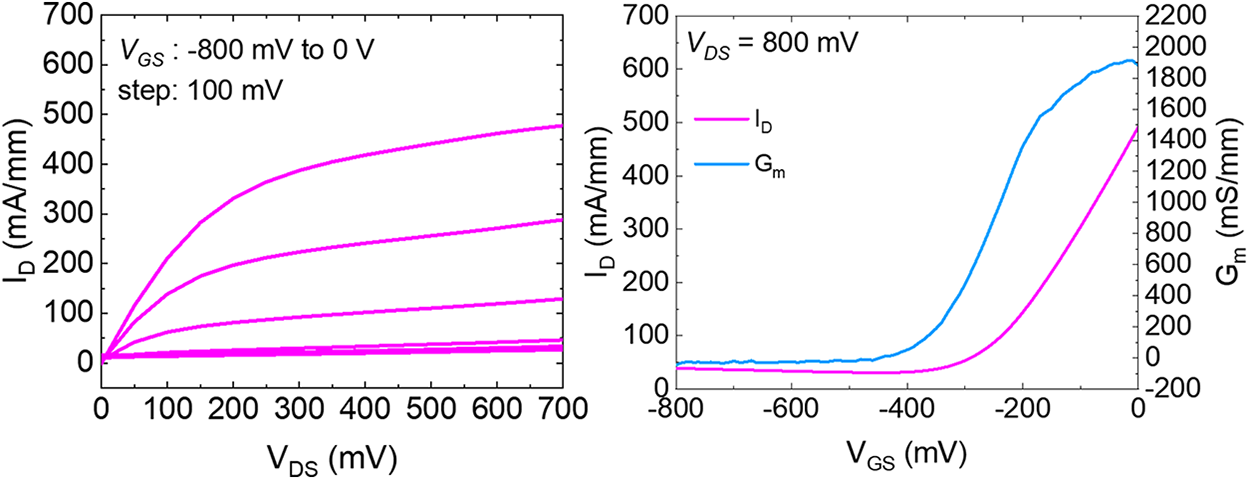
The top and cross-sectional view of the fabricated 2-finger gate configuration InAlAs/InGaAs/InAs InP-HEMT with LG = 80 nm is presented in the previously published conference article [Reference Younes, Samnouni, Lepilliet, Wichmann, Ducournau and Bollaert3]. Transistors with different gate widths of WG = 2 × 4 µm, 2 × 8 µm, and 2 × 12 µm were measured. The measurement results of the WG = 2 × 8 µm transistor were previously presented in [Reference Younes, Samnouni, Lepilliet, Wichmann, Ducournau and Bollaert3]. In this section, we will present the static and dynamic measurements of the WG = 2 × 4 µm transistor. DC measurements show a maximum drain current Id -max of 450 mA/mm with a corresponding transconductance gm of 2000 mS/mm (Fig. 10).
Output characteristic (ID-VDS) and transconductance of a 2-finger gate configuration InAlAs/InGaAs/InAs InP-HEMT with LG = 80 nm and WG = 2 × 4 µm.

Small-signal analysis was performed on the fabricated transistors in the frequency bands [250 MHz–110 GHz], [140–220 GHz], [220–325 GHz], [325–480 GHz], [500–750 GHz], and [750–1100 GHz] for a drain to source voltage VDS = 0.8 V and the gate to source voltage VGS = 0 V. To dynamically characterize our components, we will first calibrate the measuring equipment using the on-wafer mTRL calibration kit designed in the previous section. As previously discussed, the mTRL will only adjust the reference plane of the measurement closer to the active part of the device. Figure 11 shows the magnitude of the measured S-parameters (without de-embedding) of the same transistor having LG = 80 nm and WG = 2 × 4 µm for all measured frequency bands. In the literature, the determination of the gains and their associated figures of merit, fT and f max, are achieved with the open-short de-embedding method, described in [Reference Koolen, Geelen and Versleijen18]. It allows to remove the effect of parasitic elements surrounding the transistor and isolate the active part of the device. For this reason, we fabricated open and short standards directly on the wafer. These standards are also measured using the on-wafer mTRL. The short-open de-embedded S-parameters correspond to the “with de-embedding” values in Fig. 11. We notice a continuity in the S-parameter measurements over all the measured frequency bands.
Magnitude of the S-parameter measurements with and without de-embedding of InP-HEMT (LG = 80 nm, WG = 2 × 4 µm) over the frequency bands [250 MHz–110 GHz], [140–220 GHz], [220–325 GHz], [325–480 GHz], [500–750 GHz] and [750–1100 GHz].

Furthermore, from the measured S-parameters, we extracted Mason’s unilateral gain U, the Maximum Stable Gain/Maximum Available Gain MSG/MAG and the short-circuit current gain |h 21|2, as shown in Fig. 12. To understand the impact of de-embedding on the results, we first determined the f max and fT without de-embedding, obtaining values of 668 and 311 GHz from Mason’s unilateral gain U and the short-circuit current gain |h 21|2, respectively. The cut-off frequencies are measured at the 0 dB transition for each of the different gain curves, with U and MSG/MAG curves transitioning at the same frequency. After de-embedding, we obtain a precise de-embedded f max of 789 GHz and a de-embedded fT of 320 GHz. While the de-embedding had a minimal effect on the measured fT, it significantly improved the f max. This improvement is attributed to the removal of more parasitic elements through the de-embedding, enhancing the device’s performance. Despite this, it is not straightforward to conclude whether the de-embedding procedure is always necessary.
Measured and extrapolated Mason’s unilateral gain U, Maximum Stable Gain/Maximum Available Gain MSG/MAG, k-factor and short-circuit current gain |h21|2 with and without de-embedding of InP-HEMT (L G = 80 nm, WG = 2 × 4 µm) from 250 MHz to 1.1 THz.

A second question concerns the validity of the extrapolations of the gains at −20 dB/dec from standard measurements up to 110 GHz. This technique is used by several authors and allows to determine the cutoff frequencies f max and fT. Using the de-embedded S-parameters, the extrapolated values were f max = 557 GHz and fT = 290 GHz. This comparison revealed a discrepancy between the direct measured and extrapolated from the [250 MHz–110 GHz] range cut-off frequencies, indicating that higher frequency measurements provide more accurate characterizations of the transistor’s performance.
Table 2 presents a comparison between the measured and [250 MHz–110 GHz] extrapolated fT for the different transistor widths after applying the de-embedding procedure. A discrepancy between the measured and extrapolated cut-off frequencies was observed consistently across multiple devices. It can be observed that the extrapolation becomes less accurate when fT increases. The difference between the measured and extrapolated fT increases from around 30 GHz to almost 100 GHz when the width increases. Similarly, Table 2 also presents a comparison between the measured and [250 MHz–110 GHz] extrapolated f max for the different transistor widths after applying the de-embedding procedure. We noticed that the extrapolation also becomes less accurate when f max increases, but the difference between the measured and [250 MHz–110 GHz] extrapolated f max is more noticeable than that of the fT. It increases from 100 GHz to almost 240 GHz when the width decreases. This significant discrepancy between the extrapolated and measured values can be attributed to the semi-log scale used when obtaining high cut-off frequencies.
Comparison between measured fT/f max and [250 MHz–110 GHz] extrapolated fT/f max

Conclusion
In this work, we investigated on-wafer transistor characterization up to 1.1 THz by optimization of the transistor’s coplanar accesses up to the THz range using a ground-to-ground distance optimization. Our results showed that for a ground-to-ground distance of 11.5 µm, we can maintain a favorable transmission coefficient (−1 dB at 1 THz) and a stable 50 Ω characteristic impedance across all the frequency band. The final topology of the optimized CPW was used to develop a large band on-wafer mTRL calibration kit to characterize one and the same transistor and measure its precise cut-off frequencies.
This calibration kit was validated by measuring a separate ΔL = 100-µm coplanar line from 250 MHz to 1.1 THz. Then, 80 nm gate InAlAs/InGaAs/InAs high-electron-mobility transistors on InP substrate with different gate widths were developed and measured up to 1.1 THz. It is important to mention that the same transistor was measured on six different on-wafer test benches [250 MHz–110 GHz], [140–220 GHz], [220–325 GHz], [325–480 GHz], [500–750 GHz], and [750–1100 GHz]. S-parameters of the transistor are also corrected by a short-open de-embedding procedure. This enables us to compare the resulting S-parameter measurements with and without de-embedding and extract the different transistor gains with and without de-embedding.
From the different gains, we extracted the figures of merit f max and fT. The impact of the de-embedding procedure on the measured fT appears to be relatively minor, while a significant evolution is evident on the measured f max. This evolution is attributed to the removal of more parasitic elements through the correction process, leading to an improvement in overall performance. Nevertheless, determining the necessity of the de-embedding is not a straightforward conclusion to draw. In addition, we compared the measured cut-off frequency values with the extrapolation following −20 dB/decade slope from the measurements in the [250 MHz–110 GHz] frequency range.
Acknowledgements
This work is supported by Contrat de Plan Etat-Région (CPER) Wavetech at Hauts de France, and by the IEMN Flagships: Micro-Nano devices and Telecom UHD (Ultra-High-Data-rate). The Contrat de Plan Etat-Region (CPER) WaveTech is supported by the Ministry of Higher Education and Research, the Hauts-de-France Regional council, the Lille European Metropolis (MEL), the Institute of Physics of the French National Centre for Scientific Research (CNRS) and the European Regional Development Fund (ERDF). The fabrication of the devices is supported by the French national micro-nano-fabrication network (RENATECH), and characterization is supported by the CHOP platform (High frequency and Photonics characterization center) at the IEMN. The nano-fabrication is also supported by the Equipex+Nanofutur program, under the project IA-21-ESRE-0012 operated by the ANR.
Competing interests
The author(s) declare none.