Introduction
Nowadays, wireless electronic devices are part of our society, in our homes, offices, and factories. They are more efficient and more connected to the Internet. The current trend foresees a major increase of such devices, which will impose a tremendous challenge to enhance the power consumption and extend the lifetime of their batteries. Indeed, the next generation of electronic devices will be entirely wireless, and will be used in hard-to-reach and deep places, which will make maintenance operations on batteries very difficult. So, the only alternative is to use wireless charging to extend the lifetime of their batteries or even to develop battery-free devices [Reference Talla, Kellogg, Gollakota and Smith1].
RF energy harvesting is the most appropriate technology for powering wireless devices, especially if they are placed in low-light environments or difficult-to-access areas for electrical wiring. The key component of RF energy harvesting system is the rectenna. It consists of a receiving antenna and a rectifier to convert the received RF energy to dc power [Reference Takhedmit, Cirio, Merabet, Allard, Costa, Vollaire and Picon2–Reference Khemar, Kacha, Takhedmit and Abib9]. The purpose of this paper is to design and experiment a compact rectenna on low-cost substrate capable of achieving sufficient output voltage, 2.5 V at least, to remotely supply a wireless sensor from few μW RF power so as to be as close as possible to the ambient conditions. Generally, the receiving antenna takes a lot of space, it is therefore essential to reduce its size to achieve a fairly compact rectenna. Fractal shapes provide several enhancements on patch antenna, they enable to reduce the size of antennas and to improve their bandwidth [Reference Farswan, Gautam, Kanaujia and Rambabu10,Reference Zeng, Andrenko, Liu, Li and Tan11]. On another side, reducing the size of the rectenna is not sufficient, the efficiency and/or the DC voltage of the harvester is also important. Indeed, the RF-to-dc conversion circuit is a crucial part of the rectenna that will set the output electrical voltage and power. Most reported rectennas have been designed using various rectifier topologies such as single series rectifier [Reference Lu, Yang, Li and Wang12], full-wave Greinacher rectifier [Reference Song, Huang, Zhou, Zhang, Yuan and Carter13] and Villard doubler [Reference Arrawatia, Baghini and Kumar14]. In terms of output DC voltage, other topologies are more interesting. These structures consist in cascading several voltage-doubler stages, which dramatically increases the DC voltage [Reference Takhedmit, Saddi, Karami, Basset and Cirio6,Reference Congedo, Monti, Tarricone and Bella15]. An efficient dual-diode rectenna was reported in [Reference Takhedmit, Cirio, Merabet, Allard, Costa, Vollaire and Picon2]. A global efficiency, higher than 80% and a DC output voltage of 2.6 V over a 1050-Ohms resistive load, has been achieved at a power density of 220 μW/cm2. A six-stage Cockcroft–Walton rectenna operating at 2.45 GHz was reported in [Reference Takhedmit, Saddi, Karami, Basset and Cirio6]. The measured DC voltages of 1, 2, and 3 V are obtained at 1.53, 3.5, and 8 μW/cm2 power densities, respectively. This rectenna was used to start-up an electrostatic-vibration energy-harvester by RF waves. Authors in [Reference Olgun, Chen and Volakis J16] have proposed an RF harvesting module containing a 3×3 miniaturized antenna array and operating at the 2.45-GHz ISM band. It delivers an output DC voltage of 1.836 V at 0 dBm input power.
In this paper, we propose a compact stacked rectenna array capable of harvesting wireless power from low-power level, in the range of μW for powering a wireless sensor node. The antenna and the rectifier topology are chosen to give the highest output voltage with the minimum size. Thus, the use of fractal antenna is a good trade-off between size and gain. In addition, a differential-output rectifier based on a cascaded Dickson voltage multiplier is introduced, this design provides a high output voltage with various low RF input power levels. The 2 × 2 (four cells) and 3 × 3 (nine cells) series-connected rectenna arrays are fabricated and measured. The measured results show that the nine cells rectenna array provides a voltage of 2.79 V at a low-power density of 1 μW/cm2 which is well above the prior art. This rectenna is used for the first time to remotely supply a temperature and acceleration wireless sensor with a power density as small as 1 μW/cm2. The experiment is presented in this paper and results are given and discussed. This paper is organized as follows: section Basic cell rectenna design describes the design procedure of the basic cell rectenna. The experimental results of the different rectenna arrays and the wireless sensors data transmission are given in section Rectenna arrays and measurements. The conclusion is drawn in section Conclusion.
Basic cell rectenna design
The rectenna array is designed to harvest energy from the ISM band. In order to obtain a compact and efficient rectenna array, the basic cell rectenna must be as compact as possible and with a high sensitivity at low input power levels. In this section, more details about the design steps of the proposed rectenna are introduced and discussed.
Fractal antenna design
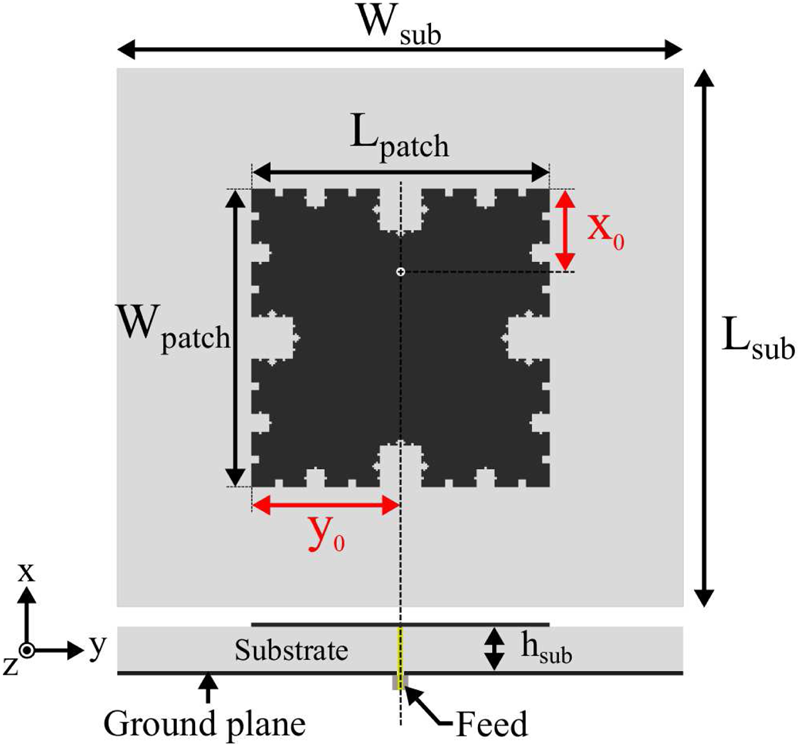
The proposed antenna consists of a third iteration Koch fractal geometry. Compared to conventional patch antenna design, the bandwidth enhancement and size reduction are the main advantages. The different iterations are generated by scratching each side of the square by a Koch curve, which decreases the size of the rectenna. The fractal curves are calculated by two parameters: IO (iteration order) and IF (iteration factor). IO represents the number of times that the starter shape has been fractalized and IF represents the reduction factor of each iteration. At each iteration, the fractal curves become smaller and smaller, which can sometimes lead to a manufacturing limitation. For that, an iteration limit must be taken into consideration. Here, the fractal shape is based on a square patch with length L = 26.4 mm, IO = 3, and IF = 0.3. The antenna is built on a standard FR-4 substrate with a dielectric permittivity (εr) of 4.3, a thickness (h) of 1.6 mm, and a loss tangent (tanδ) of 0.02. As mentioned above, fractal shape is used to reduce the size of the antenna. For comparison, a square patch antenna designed on a FR-4 substrate and operating at 2.45 GHz has a dimension of 29 × 29 mm2 [Reference Balanis17]. Here, the proposed fractal antenna has a dimension of 26.4 × 26.4 mm2, which means that a size reduction of 17% is achieved. For measurement, the antenna is fed using a 50-Ω coaxial probe. After that, the antenna is connected to the rectifier through a coppered pin via. The coaxial probe is placed along the X-axis in order to excite linear polarization. The feeding position is located at x 0 = 8.06 mm and y 0 = 13.2 mm. The antenna is designed and optimized with Ansoft HFSS software. The main configuration is shown in Fig. 1.
Configuration of the third iteration Koch fractal antenna. The antenna parameters are: W sub = 55 mm, L sub = 50 mm, L patch = 26.4 mm, W patch = 26.4 mm, X 0 = 8.06 mm, Y 0 = 13.2 mm, h sub = 1.6 mm.

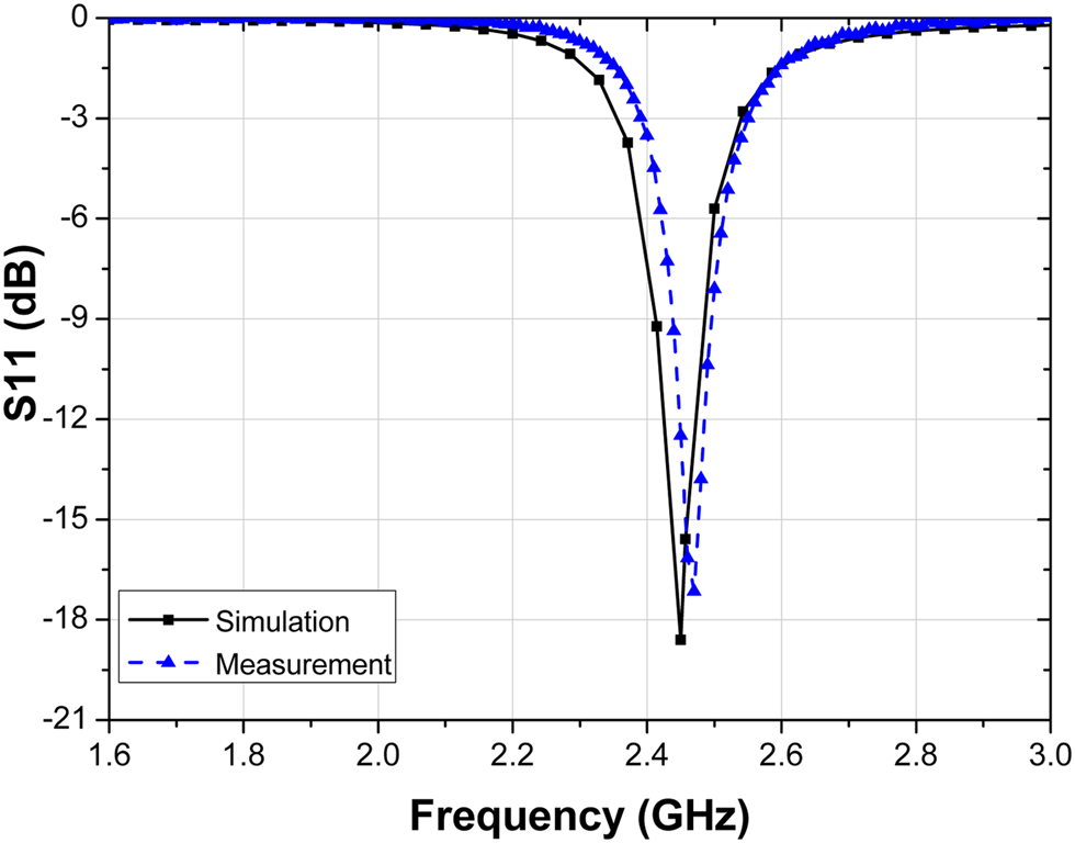
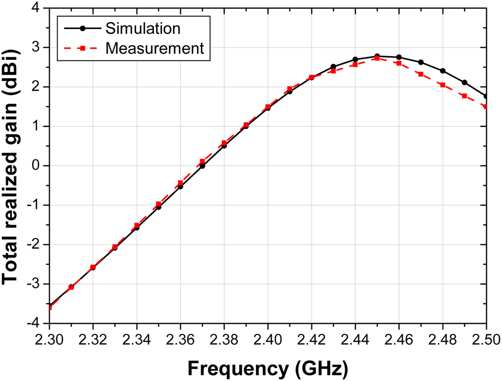
The measured and simulated reflection coefficients (S 11) are shown in Fig. 2. The measure is around −17 dB at 2.45 GHz and the −10 dB bandwidth is 2%, which covers the ISM band. The input impedance of the antenna at the operating frequency is 52.18-j10.83 Ω. The antenna is well matched with the 50-Ω impedance. The antenna was measured inside an anechoic chamber to determine the realized gain. Figure 3 shows the simulated and measured realized gains over frequency. The simulated gain at 2.45 GHz is 2.77 dBi, while the measured one is 2.72 dBi, which shows a good agreement between simulation and measurement. The ground plane, placed between the antenna and the rectifier, limits the backward radiation and allows to place the rectifier close to the antenna without decreasing the gain.
Simulated and measured reflection coefficients of the fractal antenna, simulation (solid line), and measurement (dashed line).

Simulated and measured realized gain versus frequency of the fractal antenna, simulation (solid line), and measurement (dashed line).

Rectifier design
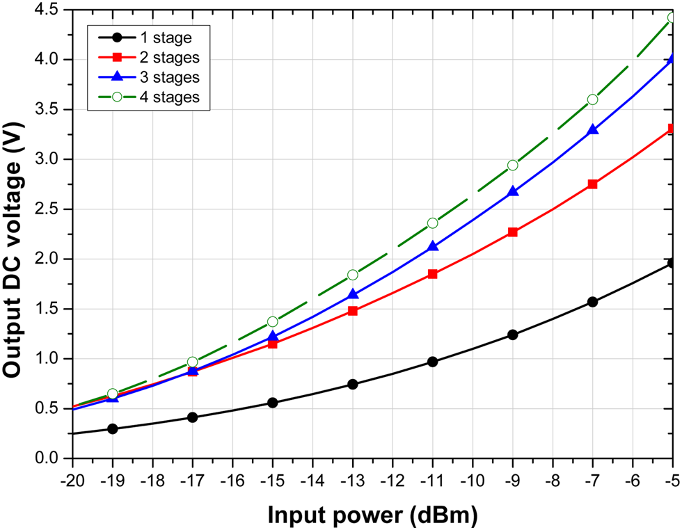
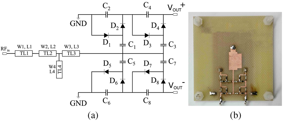
The rectifier circuit is a key part of the rectenna device. It is composed of an input filter, a rectifying diode, and a dc output filter. There are several types of rectifier topologies such as series-mounted diode, shunt-mounted diode, voltage doubler rectifier, and multiplier circuits. The choice of the topology mainly depends on the intended application. In this paper, a high output voltage from low input power levels, in the μW range, is targeted. Toward this goal, a combination of multiplier circuits and full-wave rectification is used. It consists of cascading two stages of a Dickson voltage multiplier on each branches of a full wave rectifier. This choice is relevant for the targeted application. Indeed, unlike conventional topologies in series or in shunt, the output quantity which is optimized in the case of cascaded structures is the output DC voltage. This is more appropriate for the intended application, where the aim is to deliver a DC voltage of at least 2.5 V across a capacitor load at as low as possible RF power level. This is not compatible with conventional single-diode topology rectifiers where the optimization criterion is often the maximization of the RF-to-dc conversion efficiency across a resistive load of few k-Ohms to few tens of k-Ohms. Indeed, the output voltage for this kind of rectifiers, even when the output is opened (high resistive load), is much lower than that which a multi-stage structure can deliver. The open circuit voltage is equal to twice the voltage at the terminals of an optimal load. Figure 4 shows the simulated output voltage against RF power level for several multi-stage rectifiers with different number of stages from 1 to 4. For high-power levels, the output voltage increases when the number of stages increases. For low-power levels, it can be seen that the three-stage and the four-stage rectifiers provide only a few more millivolts compared to the two-stage rectifier. The losses increase with the number of stages and the output voltage no longer increases. The number of stages has been limited to 2, which reduces the number of lumped elements and the losses. The complete configuration of the rectifier is shown in Fig. 5. The power sensitivity is enhanced and a good power handling capability is achieved by using the mechanism of full-wave rectification. The principle behind Dickson voltage multiplier is described for the positive branch as follows: during the negative half cycle of the input RF wave, the odd-numbered capacitors C 1 and C 3 are charged to a voltage equal to the input RF signal across diodes D 1 and D 3. During the positive half cycle, the even-numbered capacitors C 2 and C 4 get charged with opposite polarities through forward-biased diodes D 2 and D 4, the same principles apply to the negative branch with a reverse polarity.
Simulated output voltage for several multi-stage topologies.

(a) Topology of the T-junction filter and the dual cascaded Dickson voltage multiplier. The filter parameters are: W 1 = 3.01 mm, L 1 = 3 mm, W 2 = 5 mm, L 2 = 5.33 mm, W 3 = 5 mm, L 3 = 5.33 mm, W 4 = 8.66 mm, and L 4 = 2.55 mm. (b) Photograph of the fabricated rectifier.

A Schottky diode SMS 7630-079LF from Skyworks is selected for the multiplier due to its low threshold voltage required for small input signals, a forward voltage of 60–120 mV at 0.1 mA and a junction capacitance C j0 = 0.14 pF; the package parasitic elements were taken into account for the design process. In order to improve the accuracy, the chip capacitors are modeled using S-parameters files (S2P) provided by Kemet Electronic Components. The Schottky diodes have a non-linear behavior; they could generate some high-order harmonics that may be radiated by the antenna. To reject these harmonics, a band-pass filter is usually inserted between the antenna and the rectifier. Here, a 2.45 GHz T-junction filter is placed between the fractal antenna and the multiplier circuit to block the high-order harmonics.
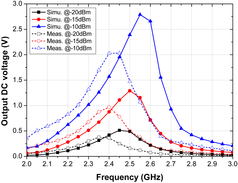
The simulation and optimization of the RF-to-dc rectifying circuit was performed on Keysight's ADS software. Once the circuit topology and that of the input matching circuit were chosen, we used an electromagnetic/circuit cosimulation to design and optimize the conversion circuit. Momentum simulator for the distributed part (line sections, stub, etc.) and Harmonic Balance simulator for the lumped linear and non-linear components (Schottky diode, capacitors, etc.) were used. At each iteration, a new layout is generated and then simulated using Momentum. A scattering parameters matrix is performed and then exported toward Harmonic Balance in order to co-simulate the full conversion circuit. As proof of concept, a rectifier prototype was printed on a FR-4 substrate with a dimension of 55 × 50 mm2. The goal here is to maximize the output voltage of the single rectenna element. Indeed, to supply a battery-free wireless sensor node, the harvested energy will initially be stored in a capacitor before being used to power the wireless sensor's electronic functions. The voltage across the storage capacitor should be around 2.5 V. The measured and simulated open circuit output voltages at three input power levels (−20, −15, and −10 dBm) are shown in Fig. 6. We can observe, at the operating frequency, measured voltages of 2 V at −10 dBm, 0.77 V at −15 dBm, and 0.25 V at −20 dBm.
Rectifier output voltage versus frequency at different input power levels.

Single-cell rectenna prototype
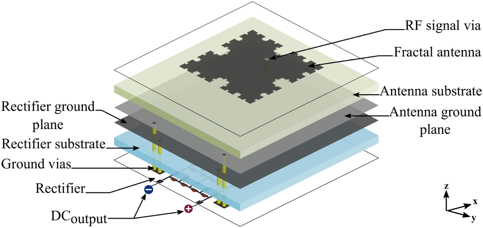
As mentioned in section Fractal antenna design, the bottom-side of the antenna is an interesting location to put an RF-to-dc rectifier without inducing any interference with the antenna radiation pattern. For that, the previous fractal antenna was stacked back-to-back with the designed RF-to-dc circuit. Interconnecting vias connect the RF signal ports and ground planes between the antenna and the rectifier. The complete rectenna 3D view is shown in Fig. 7. The overall dimensions of the single rectenna are 55 × 50 ×3.2 mm3.
Three-dimensional view of the basic cell rectenna (55 × 50 mm2).

Rectenna arrays and measurements
Rectenna association
Usually, a single rectenna does not deliver enough voltage/power to supply electronic devices, especially in a small RF power environment. To improve the rectenna output (voltage and/or power), the use of rectenna array is an effective way to increase the captured RF power and to deliver a greater DC output voltage. Here, four and nine cells rectenna arrays were studied: the cells are connected in series to form 2 × 2 and 3 × 3 rectenna arrays. In this configuration, each cell independently receives the RF power that will be converted into a dc power. Then, the converted power of each cell will be added to deliver a much higher voltage than a single rectenna cell. The proposed rectenna array is built by stacking back to back two layers of antennas and rectifiers, respectively. Each rectifier of the array is connected with its corresponding antenna. The inter-element spacing between cells was optimized according to the mutual coupling between antennas. The best trade-off between the total realized gain (thus the number of elements) and the dimensions is obtained for a distance of about 14 mm between antenna elements.
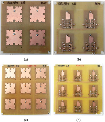
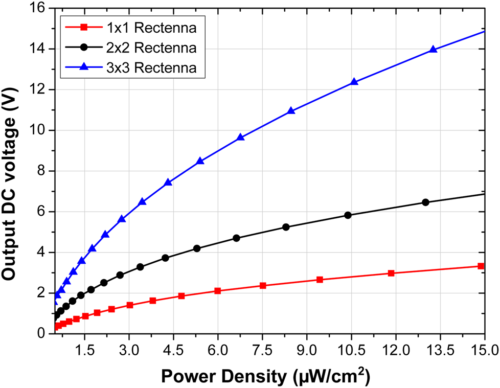
In order to decrease the coupling between the different antenna elements, we made slots on the back side (ground plane) so that each antenna element has its own ground plane. We made the same slots on the rectifier substrate so as to decrease the leakage currents. Each of the elementary conversion circuits has its own ground plane. In the final realization, the ground plane of each conversion circuit is connected only with the ground plane of the associated antenna element. Figure 8 shows the four and nine cells rectenna arrays prototypes. The measured output voltage versus surface power density for the three rectennas (one cell, four cells, and nine cells) is depicted in Fig. 9. Results show clearly a significant increase of output voltage according to the number of cells. The output dc voltage increases when the power density also increases. However, the evolution of the output voltage for the nine cells rectenna is faster than the others. The voltage goes from 1.5 to 5.6 V for the four cells rectenna versus 2.79 to 12 V for the nine cells rectenna ata power density of 1 and 10 μW/cm2, respectively.
Photographs of the fabricated prototypes. (a) Top view of four cells rectenna (86 × 91 mm2). (b) Bottom view of four cells rectenna. (c) Top view of nine cells rectenna (127 × 131 mm2). (d) Bottom view of nine cells rectenna.

Measured output voltage against power density for the different rectenna prototypes.

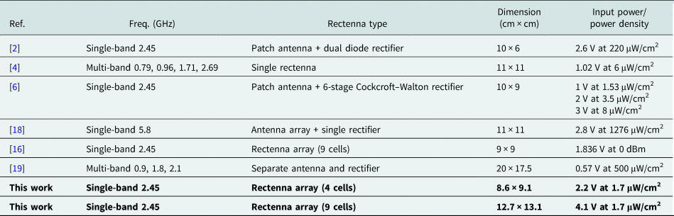
Table 1 illustrates the performance comparison with recently reported designs. It can be seen that the proposed rectenna array has a smaller size than some single rectenna and deliver a higher output voltage with a lower input power density than other rectenna array, validating the benefit of this topology.
Comparison with other reported designs

Wireless sensors data transmission experiment
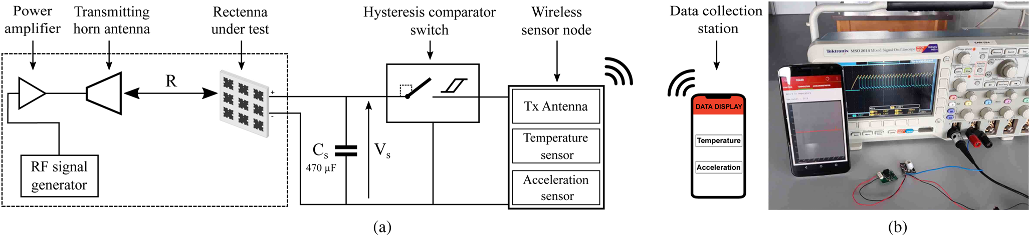
The nine cells rectenna array is used as a power supply for a battery-free temperature and acceleration sensor node which sends the measured data to a smartphone by Bluetooth Low Energy (Fig. 10). A signal generator and a 30 dB power amplifier connected to a horn antenna were used to transmit the 2.45 GHz RF power. The rectenna was aligned with the transmitting antenna with a distance R = 1.5 m. The rectenna array was then connected to a 470 μF storage capacitor C s. A hysteresis comparator switch was connected to the capacitor C s to control the power supply of the wireless sensor node.
(a) Schematic of the sensors data transmission experiment. (b) Photograph of the voltage evolution on Cs and data display on smartphone.

The switch is controlled by the voltage across capacitor C s (V s). When V s reaches 2.5 V, the switch is closed supplying the wireless sensor node, which sends data via a Bluetooth link to a data collection station (smartphone). The voltage across C s decreases until it reaches 1.85 V; then, the switch is opened, and the wireless sensor node disconnected. The capacitor is recharged by the rectenna until a new measurement cycle is performed.
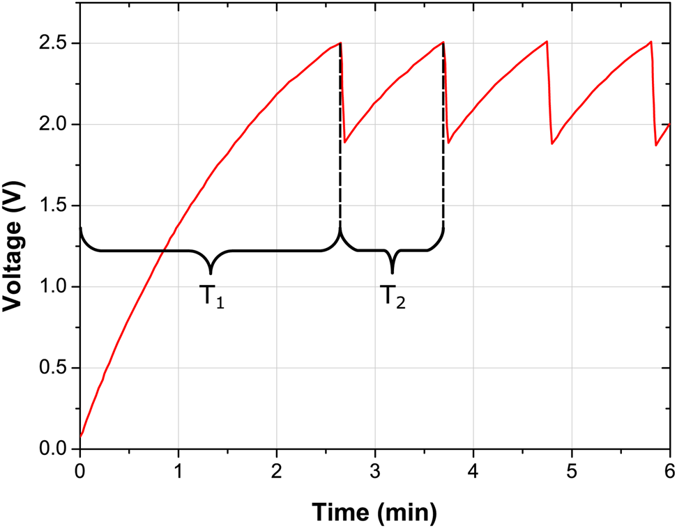
Figure 11 represents the measured voltage evolution as a function of time on capacitor C s at a power density of 1.7 μW/cm2. We notice that the initial charging (T 1) from 0 to 2.5 V takes about 2.7 min, the energy stored is about 1468.75 μJ. When the voltage reaches 2.5 V, the switch is turned-on and the wireless sensor circuit sends the measured temperature and acceleration to a smartphone (data collection station). The power consumption for measurement, analysis, and data transfer is 664.46 μJ. Only 1.1 min is then required between each measurement cycle.
Measured voltage evolution on Cs as a function of time.

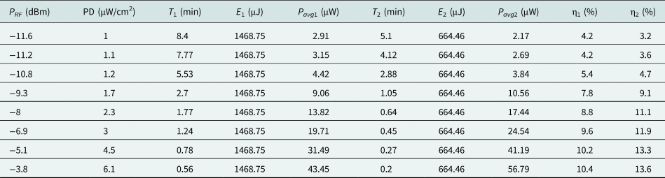
Several measurements were conducted with different power density values. The results are summarized in Table 2, where P RF is the input power, PD is the power density received by the nine-cell rectenna, T 1 is the initial charging duration from 0 to 2.5 V, E 1 is the energy stored in the capacitor for the first cycle, P avg1 is the harvested power during the first cycle; T 2 is the duration of a following cycle, E 2 is the accumulated energy during this cycle, and P avg2 is the average harvested power during this cycle.
Results summary of the experiment

The power density (PD) is calculated as follows:
 $$ PD={P_{t}*G_{t} \over 4* \pi * D^{2} }, $$
where P t is the transmitting antenna power, G t is the transmitting antenna gain (12 dBi), and D is the distance from the transmitting antenna and the receiving antenna (1.5 m).
The efficiencies η1 and η2 of the first and second cycles are calculated by the following equations:
 $$ \eta_{n}(\%) =100\times{P_{avg\ n} \over P_{RF}}=100\times{P_{avg\ n} \over PD*Ae} $$
 $$ Ae ={\lambda^{2}*G \over 4\pi}, $$
where  $n=\lbrace 1, 2\rbrace $, P RF is the RF power received by the antenna, Ae is the effective antenna aperture, λ is the wavelength, and G is the antenna gain. The total RF power (P RF) is calculated as the product of the power density by the effective area of the array, obtained by simulation. The HFSS simulations showed a gain of 7.6 dBi at 2.45 GHz which corresponds to a total effective area of 68.7 cm2.
In order to obtain an estimation of the power required by the sensor to perform the physical measurements of temperature and acceleration and to transmit the data over a wireless link, we have calculated the average power from the energy consumed by the sensor. Under the illumination conditions of 1 μW/cm2 power density, the sensor requires 2.91 μW during the T 1 phase and 2.17 μW during the T 2 phase. The results show that the wireless sensor operates from a very low-power density of 1 μW/cm2, with one data transmission every 5 min and an average efficiency about 4.2% for the first cycle and 3.2% for the second cycle. The efficiency grows up to 10.4 and 13.6% at 6.1 μW/cm2 for the first and second cycles, respectively.
Conclusion
Rectenna arrays with four and nine cells have been proposed and experimentally characterized. The rectenna arrays were built around a stacked fractal antenna and a Dickson voltage multiplier resulting in small size and high output voltage devices particularly well adapted for low RF power levels. It is demonstrated that the rectenna array can achieve at 1.7 μW/cm2 an output voltage of 2.2 and 4.1 V for the four and nine cells rectenna arrays, respectively. The nine cells rectenna was tested to remotely power a wireless sensor node, which performs a measurement cycle (measure, analysis, and Bluetooth Low Energy emission) every 1 min at a power density of 1.7 μW/cm2 and every 5 min at 1 μW/cm2. With the high output voltage in low RF power environments, the designed rectenna can be used to power low consumption wireless devices. As demonstrated, the high output voltage at low-power densities that the proposed rectenna array allows, combined with the hysteresis comparator switch with very low losses, could represent a relevant solution for supplying battery-free wireless sensors.
 Hichem Mahfoudi received his Master degree in the field of Instrumentation Engineering from the Faculty of Electronic and Computer Sciences, USTHB University, Algiers, Algeria, in 2012. Actually, he is working toward the Ph.D. degree in the same faculty. His research interests include microwave circuits, RF energy harvesting, and antennas.
 Hakim Takhedmit received the State Engineer degree in Electronics from the Ecole Polytechnique d'Alger (Algeria) in 2005 and his Ph.D. degree in Electrical Engineering from the Ecole Centrale de Lyon (France) in 2010. He joined the ESYCOM laboratory (FRE 2028) in 2010 and worked as a Research Assistant until 2013. He is currently an Associate Professor at the University Paris-Est Marne-la-Vallée (France). His research focuses on the design, the modeling, and the experiments of Wireless Power Transfer (WPT) and RF Energy Harvesting. He is also interested in the numerical modeling, the remote powering of low consumption wireless sensors, and the Power Optimization Waveforms for WPT.
 Mohamed Tellache was born in Algeria in 1960. He received the Engineer degree in Electrical Engineering from the Ecole Nationale Polytechnique of Algiers in 1985. He received his Master degree in 1988 in Electronic Communication from Ottawa University, Canada, and the Ph.D. degree in 2008 in Telecommunications from USTHB, Algeria. During 1995/1998, he spent 18 months at the Electronics Laboratory of INP-ENSEEIHT, Toulouse, France, working principally on microwaves technology and modeling. He was the Head of the High School of Technology during 2009–2012 and before this, the Head of the Telecommunications Department in USTHB. Presently, he is a Professor of Electrical Engineering at the faculty of Electronics and Computers of USTHB, working on the development of new algorithms for modeling microwave devices, numerical methods for electromagnetism, full-wave characterization of microwave circuits, microwave, and components design and communication systems.
 Sebastien Boisseau received his Ph.D. degree in France in 2011. His Ph.D. dissertation dealt with energy harvesting from ambient vibrations by using charged dielectrics (electrets). He joined CEA-LETI laboratories, Grenoble, in 2011 to work on energy harvesting and wireless sensor systems powered by ambient energy. His research interests include mechanical energy harvesters, innovative couplings, power management circuits, low-power electronics, and smart materials. He is the co-author of over 40 publications in journals and conference proceedings and of more than 15 patents.