
Introduction
Often referred to as the blueprint to life, deoxyribonucleic acid, or DNA, contains the set of instructions required for the development and functioning of all living organisms. Given the importance of this molecule, it is hardly surprising that there has been significant interest in the development of low-cost methods capable of rapidly reading the sequence of nucleobases in a DNA molecule.[Reference Shendure and Ji1–Reference Schadt, Turner and Kasarskis4] The development of such a DNA sequencing technique promises to revolutionize modern healthcare with applications ranging from rapid disease diagnosis and treatment to biosecurity and fundamental biological research.[Reference Norris, Workman, Fan, Eshleman and Timp5, Reference Stankiewicz and Lupski6]
Many methods to sequence DNA have been proposed, however, a technique known as sequencing by synthesis has come to dominate the current market.[Reference Mardis7] This approach typically works by adding and subsequently detecting fluorescently labelled nucleotides to a short fragment of the DNA. This process is repeated for many copies of the strand and the sequence is reconstructed by connecting overlapping regions. While this technique has been significantly optimized over the past decade, the relatively complex sample preparation, short read lengths, and expensive reagents required, place a fundamental limit on the minimum speed and cost that can be achieved using this sequencing method.[Reference Chaisson, Wilson and Eichler8, Reference Branton, Deamer, Marziali, Bayley, Benner, Butler, Di Ventra, Garaj, Hibbs, Huang, Jovanovich, Krstic, Lindsay, Ling, Mastrangelo, Meller, Oliver, Pershin, Ramsey, Riehn, Soni, Tabard-Cossa, Wanunu, Wiggin and Schloss9] Moreover, as sequencing by synthesis relies on reconstructing the DNA sequence from short read fragments it is not suited for de novo sequencing or sequencing DNA containing large regions of repetition.
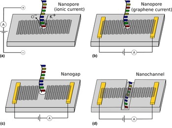
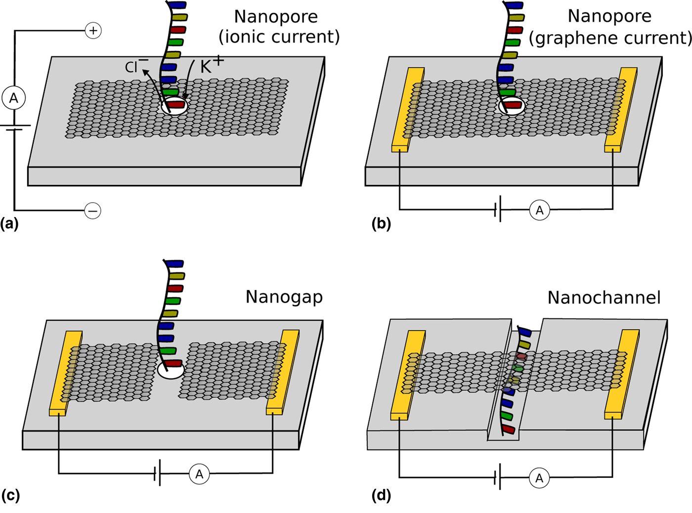
An alternate sequencing technique that has recently gained significant traction is nanopore-based DNA sequencing.[Reference Branton, Deamer, Marziali, Bayley, Benner, Butler, Di Ventra, Garaj, Hibbs, Huang, Jovanovich, Krstic, Lindsay, Ling, Mastrangelo, Meller, Oliver, Pershin, Ramsey, Riehn, Soni, Tabard-Cossa, Wanunu, Wiggin and Schloss9–Reference Wang, Yang and Wang11] These devices consist of a nanometer-sized hole in an impermeable membrane that separates two chambers of an electrolytic solution [Fig. 1(a)]. When a voltage is applied across the membrane, ions flow through the nanopore resulting in a measurable current. Due to its negative charge, DNA can be electrophoretically driven through a nanopore by the application of an electric field.[Reference Kasianowicz, Brandin, Branton and Deamer12] The presence of DNA in the pore blocks the passage of ions leading to a change in the ionic current. Due to the unique properties of each nucleobase (such as size and shape), these current changes are base specific, thus enabling sequencing of DNA as it translocates through the pore.[Reference Cherf, Lieberman, Rashid, Lam, Karplus and Akeson13–Reference Venkatesan and Bashir15] Given the simple sample preparation and long read lengths of nanopore sequencing, this technology has the potential to provide low-cost, portable devices capable of rapid DNA sequencing.[Reference Branton, Deamer, Marziali, Bayley, Benner, Butler, Di Ventra, Garaj, Hibbs, Huang, Jovanovich, Krstic, Lindsay, Ling, Mastrangelo, Meller, Oliver, Pershin, Ramsey, Riehn, Soni, Tabard-Cossa, Wanunu, Wiggin and Schloss9] Indeed, nanopore sequencing has already experienced significant success and devices based on this technology are now commercially available.[Reference Mikheyev and Tin16–Reference Jain, Koren, Miga, Quick, Rand, Sasani, Tyson, Beggs, Dilthey, Fiddes, Malla, Marriott, Nieto, Grady, Olsen, Pedersen, Rhie, Richardson, Quinlan, Snutch, Tee, Paten, Phillippy, Simpson, Loman and Loose18]
(a) Schematic of ionic current DNA sequencing using a graphene nanopore. (b–d) Schematics of DNA sequencing utilizing the conductive properties of graphene as; (b) DNA translates through a nanopore in the graphene, (c) DNA translates through a nanogap in the graphene and (d) DNA translates through an adjacent nanofluidic channel.
Despite the success of nanopore sequencing, these devices suffer from several limitations. In particular, nanopore sequencing is typically pursued using biological nanopores, which have a fixed shape, limited stability, and are not suited to a massive upscaling in production.[Reference Dekker10] One solution currently being explored is to create nanopores in solid-state materials[Reference Dekker10] such as SiO2, SiNx and Al2O3. However, these pores are typically tens of nanometers thick resulting in ionic current blockades that are a convolution of the 10–100 nucleotides residing within the pore at a given time.[Reference Heerema and Dekker19] For this reason, there has been significant interest in creating nanopores in two-dimensional materials, such as graphene, for DNA sequencing.[Reference Heerema and Dekker19–Reference Garaj, Hubbard, Reina, Kong, Branton and Golovchenko22] However, fast DNA translocation rates through these nanopores have hindered single-base resolution due to large parasitic capacitance signals at high sampling frequencies.[Reference Rosenstein, Wanunu, Merchant, Drndic and Shepard23]
Given graphene's conductive properties, DNA sequencing techniques relying on detecting changes in the current in a graphene nanostructure as DNA translates through a nearby nanopore or nanochannel have also been suggested.[Reference Heerema and Dekker19] In particular, three device geometries have thus far been proposed: (i) monitor the graphene current as DNA translocates through a nanopore in the graphene ribbon[Reference Nelson, Zhang and Prezhdo24, Reference Traversi, Raillon, Benameur, Liu, Khlybov, Tosun, Krasnozhon, Kis and Radenovic25] [Fig. 1(b)], (ii) monitor the tunnelling current across a graphene nanogap as DNA translates through the gap[Reference Postma26] [Fig. 1(c)] and (iii) monitor the graphene current as DNA translates through an adjacent nanofluidic channel[Reference Min, Kim, Cho and Kim27] [Fig. 1(d)]. Importantly, utilizing the conductive properties of graphene offers the potential for high bandwidth measurements, thus enabling DNA sequencing without the need to slow DNA translocation. Additionally, unlike ionic current-based sequencing, these devices can easily be multiplexed as the current through each nanostructure can be read independently. Despite their significant promise, DNA sequencing utilizing graphene-based electronic devices has yet to be demonstrated. This has been partly due to the complex fabrication requirements of these devices that has resulted in low device yields and limited throughput.[Reference Healy, Ray, Willis, Peterman, Bartel and Drndić28–Reference Yuan, Wang, Yi, Ni, Chen and Li31] This paper reviews the general fabrication principles of graphene-based electronic sequencing devices. While each published study will inevitably use a different device design and fabrication procedure, particular focus will be given to common fabrication challenges as well as highlighting some of their potential solutions. It is hoped that this will help drive an increase in the fabrication yield and throughput of future devices hence providing a significant step toward sequencing. It is noted that reviews focusing on the mechanisms behind changes in the graphene current as DNA translates through a nearby nanopore are available elsewhere.[Reference Heerema and Dekker19, Reference Kim and Kim32]
Graphene nanopores
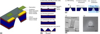
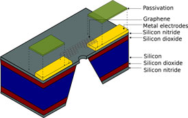
DNA sequencing devices consisting of a nanopore within a graphene nanoribbon (GNR) will be discussed first. These devices function by detecting changes in the graphene current as DNA translocates through the pore in a direction perpendicular to the graphene plane [Fig. 1(b)]. These devices should not be confused with ionic current-based graphene nanopore sequencing devices that have been extensively described elsewhere.[Reference Heerema and Dekker19–Reference Garaj, Hubbard, Reina, Kong, Branton and Golovchenko22] A schematic of the typical geometry for these devices is shown in Fig. 2(a). In particular, these devices typically consist of a SiNx window that is suspended over a SiO2 layer on a silicon substrate. Graphene and metal contact electrodes are patterned on the SiNx with a passivation layer covering the metal electrodes. A nanopore in the graphene and underlying SiNx window enables DNA translocation. These devices have been studied in many computational works and indeed nucleobase-specific changes in the graphene current have been predicted.[Reference Nelson, Zhang and Prezhdo24, Reference Saha, Drndić and Nikolić33–Reference Girdhar, Sathe, Schulten and Leburton36] Furthermore, several experimental studies have detected DNA translocation through a graphene nanopore via changes in the graphene current.[Reference Traversi, Raillon, Benameur, Liu, Khlybov, Tosun, Krasnozhon, Kis and Radenovic25, Reference Heerema, Vicarelli, Pud, Schouten, Zandbergen and Dekker30, Reference Puster, Balan, Rodrguez-Manzo, Danda, Ahn, Parkin and Drndić37] However, fabrication throughput and device yield, as well as experimental challenges such as graphene wetting and electrostatic discharge continue to hinder the development of these devices towards DNA sequencing.[Reference Heerema, Vicarelli, Pud, Schouten, Zandbergen and Dekker30]
(a) Schematic representation of graphene nanopore electronic DNA sequencing devices. (b) Schematic of the steps involved in forming SiNx windows. (c) Schematic of nanopore creation via (i) TEM drilling, (ii) electron beam lithography followed by reactive ion etching and (iii) delectric breakdown. (d) TEM images of a nanopore within a GNR created via TEM drilling.[Reference Traversi, Raillon, Benameur, Liu, Khlybov, Tosun, Krasnozhon, Kis and Radenovic25, Reference Puster, Rodrguez-Manzo, Balan and Drndić38] Figures adapted with permissions from (d) Nature publishing group[Reference Traversi, Raillon, Benameur, Liu, Khlybov, Tosun, Krasnozhon, Kis and Radenovic25] and American Chemical Society.[Reference Puster, Rodrguez-Manzo, Balan and Drndić38]

This section will begin by discussing the fabrication of suspended SiNx structures. These structures are necessary to enable nanopore formation and are also relevant for the graphene nanogap detectors discussed in the section “Graphene nanogaps.” The procedure for fabricating SiNx windows has been described elsewhere[Reference Grant, Hu and Kasemo39] and typically consists of growing a SiO2 layer on a high resistivity silicon <100> substrate then depositing low-pressure chemical vapor deposition (LPCVD) SiNx films, followed by photolithography and subsequent etching [Fig. 2(b)]. Care should be taken to ensure etching along the correct crystal orientations. A protective layer made of an easily removed polymer may be used during etching to protect features on the front side of the wafer from leakages caused by defects when etching. The SiO2 film is used to reduce capacitive coupling between the metal electrodes and silicon substrate and is generally between 0.1 and 5 µm thick. One result of this thick SiO2 layer is that, due to its compressive stress, the resulting SiNx windows can have an uneven surface topography.[Reference Healy, Ray, Willis, Peterman, Bartel and Drndić28] This can be partially reduced via thermal annealing, however, this may result in bulging of the window. Several studies have attempted to overcome these issues by growing thin SiNx films on highly insulating substrates without a SiO2 layer[Reference Lee, Kumar, Park, Cho, Kim, Lim, Kim and Kim40] or with a poly-Si[Reference Yanagi, Ishida, Fujisaki and Takeda41] layer, however, these devices may exhibit increased noise due to capacitive coupling to the substrate.
Metal electrodes are used to enable electrical contact to graphene nanodevices. Although not strictly necessary, patterning contact electrodes prior to graphene transfer is preferable as it exposes graphene to less processing. Metal electrodes are fabricated using photolithography coupled with electron beam lithography (for large and small feature sizes, respectively) followed by metal deposition and subsequent liftoff. Electron beam lithography is used to pattern electrodes over the SiNx window with local alignment markers written during this step to allow for later alignment of graphene nanostructures. Note that patterning resist over the SiNx window requires a higher dose than supported parts of the chip due to the decreased contribution of backscattered electrons. These metal electrodes must be passivated to (i) reduce faradaic currents resulting from electrochemical reactions between the electrodes and ionic solution[Reference Healy, Ray, Willis, Peterman, Bartel and Drndić28] and (ii) reduce noise resulting from capacitive coupling to the ionic solution. Several materials have been used for passivation such as SiO2/SiNx.[Reference Ivanov, Instuli, McGilvery, Baldwin, McComb, Albrecht and Edel42] Al2O3,[Reference Traversi, Raillon, Benameur, Liu, Khlybov, Tosun, Krasnozhon, Kis and Radenovic25] TiO2,[Reference Healy, Ray, Willis, Peterman, Bartel and Drndić28] h-BN[Reference Heerema, Vicarelli, Pud, Schouten, Zandbergen and Dekker30] and various polymeric films. Care should be taken to ensure proper adhesion of the passivation to metal electrodes.[Reference Temiz, Ferretti, Leblebici and Guiducci43] In general, there are two considerations to be made regarding the thickness of the passivation layer. First, the film must be thick enough to avoid pinholes in the passivation. This thickness is largely dependent on the deposition process (e.g. atomic layer deposition, electron beam evaporation, CVD, photoresist spincoating) and the chosen dielectric. Second, the passivation thickness should be thick enough to reduce noise resulting from capacitive coupling to the ionic solution. Although dependent on the dielectric used and the device geometry, the authors have found that dielectric thicknesses greater than 500 nm are required to significantly reduce this noise. Electrode passivation is routinely performed after graphene transfer and patterning to ensure that the metal electrodes can be fully passivated as well as nonactive areas of the graphene.
Perhaps, the most challenging aspect of fabrication is forming the nanopore. These nanopores are typically formed using high-energy electron irradiation from a transmission electron microscope (TEM)[Reference Traversi, Raillon, Benameur, Liu, Khlybov, Tosun, Krasnozhon, Kis and Radenovic25, Reference Heerema, Vicarelli, Pud, Schouten, Zandbergen and Dekker30, Reference Puster, Balan, Rodrguez-Manzo, Danda, Ahn, Parkin and Drndić37, Reference Puster, Rodrguez-Manzo, Balan and Drndić38] [Figs. 2(c)(i) and 2(d)]. However, this technique requires expensive equipment, expert training, and is time consuming. As such, techniques to reliably and rapidly form nanopores in graphene, SiNx, and other two-dimensional materials continue to be researched. Other techniques to create nanopores in SiNx membranes include electron beam lithography followed by reactive ion etching[Reference Verschueren, Yang and Dekker44] [Fig. 2(c)(ii)] and focused ion beam milling, including gas field ion sources such as helium ion microscopes and eutectic sources. While these techniques are only capable of reproducibly creating nanopores with diameters on the order of 15 nm and larger, nanopores shrinking methods can be used to reduce the diameter of these pores[Reference Asghar, Ilyas, Billo and Iqbal45] to sizes compatible with DNA sequencing applications. An alternate technique to scalably fabricate nanopores in SiNx relies on electric field-induced breakdown. Namely, pores with subnanometer precision can be fabricated in SiNx via feedback-controlled dielectric breakdown [Fig. 2(c)(iii)] whereby a large electric field is applied across the membrane while monitoring the leakage current.[Reference Kwok, Briggs and Tabard-Cossa46] Techniques to control the position and number of nanopores created via dielectric breakdown continue to be developed.[Reference Pud, Verschueren, Vukovic, Plesa, Jonsson and Dekker47, Reference Wang, Ying, Zhou, de Vreede, Liu and Tian48] Such formation of SiNx nanopores could then be followed by graphene transfer and nanopore formation by applying pulsed electric fields across the membrane[Reference Kuan, Lu, Xie, Szalay and Golovchenko49] to create self-aligned graphene nanopores. Alternately, this pulsed electric field breakdown technique could be used to create nanopores in freestanding graphene membranes, however, a coating layer would be required to avoid DNA sticking to the graphene prior to translocation.[Reference Kuan, Lu, Xie, Szalay and Golovchenko49]
Despite several promising studies demonstrating DNA detection via changes in the graphene current as DNA translates through a pore in the graphene,[Reference Traversi, Raillon, Benameur, Liu, Khlybov, Tosun, Krasnozhon, Kis and Radenovic25, Reference Heerema, Vicarelli, Pud, Schouten, Zandbergen and Dekker30, Reference Puster, Balan, Rodrguez-Manzo, Danda, Ahn, Parkin and Drndić37] recent works continue to cite low fabrication throughput and device yield as significant problems.[Reference Heerema, Vicarelli, Pud, Schouten, Zandbergen and Dekker30] This is no doubt in part due to the many fabrication steps required, each of which need to be optimized to return an acceptable yield. Additionally, nanopore formation using a TEM is a time-consuming process which significantly limits device throughput. Techniques to scalably create nanopores in graphene and SiNx, some of which were highlighted above, will need to continue to be developed if this sequencing approach is to continue to advance over the coming years.
Graphene nanogaps
DNA sequencing techniques based on graphene nanogaps will now be discussed. These devices function by detecting changes in the tunnelling current across a graphene nanogap as DNA translocates through the gap in a direction perpendicular to the graphene plane[Reference Puczkarski, Swett and Mol50] [Fig. 1(c)]. Similar to the geometry discussed for graphene nanopores, these devices consist of a graphene nanogap aligned with a nanopore in the underlying SiNx window. While it may be possible to use graphene as both the membrane and electrode material,[Reference Postma26] such a device would likely have limited control over the position of DNA during translocation.[Reference Lagerqvist, Zwolak and Di Ventra51] This is a particularly important consideration given the exponential dependence of tunnelling current on gap distance. Graphene nanogap sequencing devices have been studied in several computational works where nucelobase-specific changes in the tunnelling current were predicted due to different coupling strengths between the graphene and the molecular orbitals of each base.[Reference Postma26, Reference Prasongkit, Grigoriev, Pathak, Ahuja and Scheicher52–Reference Amorim, Rocha and Scheicher55] Additionally, experimental works have detected and discriminated nucleotides via changes in the tunnelling current in a scanning tunnelling microscope[Reference Ohshiro and Umezawa56–Reference Chang, Huang, He, Liang, Zhang, Li, Chen, Sankey and Lindsay59, Reference Di Ventra and Taniguchi60] and metal nanogaps.[Reference Di Ventra and Taniguchi60–Reference Pang, Ashcroft, Song, Zhang, Biswas, Qing, Yang, Nemanich, Bai, Smith, Reuter, Balagurusamy, Astier, Stolovitzky and Lindsay65] No attempts to detect DNA using tunnelling currents across a graphene nanogap have been published to date.
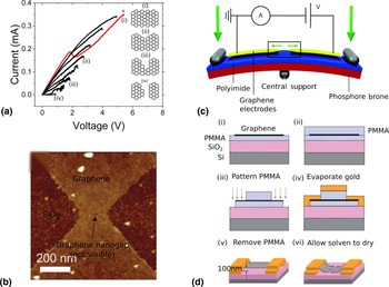
Several techniques to fabricate graphene nanogaps have been demonstrated that could conceivably be used for nanogap-based DNA sequencing.[Reference Prins, Barreiro, Ruitenberg, Seldenthuis, Aliaga-Alcalde, Vandersypen and van der Zant66–Reference Bellunato, Vrbica, Sabater, de Vos, Fermin, Kanneworff, Galli, van Ruitenbeek and Schneider69] One such technique is feedback-controlled electroburning.[Reference Prins, Barreiro, Ruitenberg, Seldenthuis, Aliaga-Alcalde, Vandersypen and van der Zant66, Reference Lau, Mol, Warner and Briggs70, Reference El Abbassi, Pósa, Makk, Nef, Thodkar, Halbritter and Calame71] Here, a voltage ramp is applied across a GNR while the current is simultaneously recorded. Large current densities in the graphene induce Joule heating which can lead to oxidation or sublimation of carbon atoms at the edges.[Reference El Abbassi, Pósa, Makk, Nef, Thodkar, Halbritter and Calame71] When this happens, the graphene resistance increases resulting in a drop in the current [asterisk in Fig. 3(a)] at which point the voltage is ramped back to zero. Repeating this process allows for the controlled formation of a nanogap across a GNR [Figs. 3(a) and 3(b)]. Recently, graphene nanogaps have also been fabricated via mechanically controlled break junctions.[Reference Caneva, Gehring, Garca-Surez, Garca-Fuente, Stefani, Olavarria-Contreras, Ferrer, Dekker and van der Zant67] Here, graphene was patterned on a flexible phosphor bronze substrate and loaded into a three-point bending configuration [Fig. 3(c)]. The graphene current is monitored during bending until a sharp drop in the conductance is observed signifying the formation of a nanogap. Another method that has been used to create graphene nanogaps relies on capillary force-induced breaking of suspended graphene.[Reference Wang, Zheng, Wang, Qiu, Guo, Shen and Yu68, Reference Patel, Carroll, Lopez, Sankararaman, Etienne, Kodigala, Paul and Postma72] In this technique, graphene is suspended across a trench in the substrate, and broken due to the surface tension of the solvent during the drying process [Fig. 3(d)].
(a) An example of the electroburning process. The first trace is shown in red. The asterisk shows the point where the graphene resistance increases indicating the onset of electroburning. The insets show schematics of the nanogap formation process during electroburning. (b) An atomic force microscope image of a graphene nanogap formed via electroburning on a SiO2 substrate.[Reference Lau, Mol, Warner and Briggs70] The graphene has been patterned into a constriction to enable controlled positioning of the nanogap. (c) Schematic of the mechanical controlled break junction setup to form graphene nanogaps.[Reference Sun, Diaz-Fernandex, Gschneidtner, Westerlund, Lara-Avila and Moth-Pouslen98] (d) Schematic of an example fabrication process to produce a graphene nanogap via capillary force induce breaking.[Reference Wang, Zheng, Wang, Qiu, Guo, Shen and Yu68] Figures adapted with permissions from (b) PCCP Owner Societies,[Reference Lau, Mol, Warner and Briggs70] (c) Royal Society of Chemistry [relevant citation added above] (d) AIP Publishing.[Reference Wang, Zheng, Wang, Qiu, Guo, Shen and Yu68]

One of the major challenges in the fabrication of these devices is the alignment of graphene nanogaps with an underlying SiNx nanopore. Graphene can be fabricated into a constriction to enable the controlled positioning of a graphene nanogap via the electroburning[Reference Lau, Mol, Warner and Briggs70] [Fig. 3(b)] and mechanically controlled break junction[Reference Caneva, Gehring, Garca-Surez, Garca-Fuente, Stefani, Olavarria-Contreras, Ferrer, Dekker and van der Zant67] techniques discussed above. Patterning of graphene into such geometries is generally done via electron beam lithography followed by etching with alignment of features down to 20 nm readily obtained using local alignment markers. Care should be taken with alignment marker position near the SiNx window. However, alignment on the order of a few nanometers would likely be required to ensure that a single tunnel junction is reproducibly aligned with a nanopore. Moreover, formation of graphene nanogaps via feedback-controlled electroburning and mechanical-controlled break junctions have to date only been demonstrated on supported or semi-supported substrates and these techniques will need to be developed for suspended graphene membranes compatible with DNA sequencing. It is noted that DNA translocation through graphene nanogaps was recently demonstrated by aligning a “micropore” in a polymeric film with the nanogap.[Reference Patel, Carroll, Lopez, Sankararaman, Etienne, Kodigala, Paul and Postma72] By doing this, the authors were able to detect DNA passing though the nanogap via changes in the ionic current, however, simultaneous monitoring of the graphene tunnelling current was not reported. While such a nanogap/micropore assembly may be useful for preliminary studies into DNA detection using graphene tunnelling currents, it is likely that sequencing devices will require more stringent control over the position of DNA as it translates through the nanogap.
The integration of electric and fluidic components is another challenging aspect in the development of graphene-based electronic sequencing techniques. For the nanopore and nanogap devices discussed above, similar fluidic designs to that used in typical ionic current nanopore experiments can be envisioned. These fluidic designs can be broadly classified into three classes; (i) a fluidic reservoir approach, (ii) a microfluidic flow cell approach, and (iii) a nanocapillary approach. For the proposed sequencing devices, electrical connections will need to be incorporated to enable measurements of the graphene current. For the fluidic reservior and microfluidic approaches this could be done by wirebonding to a printed circuit board or the incorporation of pins within the fluidic cell to directly contact the chip. Microfluidic cells have the advantage over fluidic reserviors in that they enable liquids to be pumped through the nanopore enabling pore wetting and fluidic transfer. This is a particular problem for the devices considered here since graphene is not compatible with commonly used techniques that render a nanopore hydrophilic such as Piranha solution and oxygen plasma treatment.[Reference Heerema, Vicarelli, Pud, Schouten, Zandbergen and Dekker30] The use of nanocapillaries to fluidically contact devices[Reference Arcadia, Reyes and Rosenstein75] is an appealing approach as it may enable easy electrical connection. However, it is yet to be seen whether devices can be effectively contacted and the fluid localized at the nanopore without wetting of the electrical contacts. Additionally, a nanocapillary is not suited to multiplexed measurements.
While promising results have been reported on the detection and discrimination of nucleobases via tunnelling currents in a scanning tunnelling microscope and metal nanogaps, fabrication of graphene nanogaps for tunnelling current sequencing is yet to be reported. Indeed, several studies on metal nanogaps integrated within a nanopore have cited significant difficulties in the fabrication process,[Reference Healy, Ray, Willis, Peterman, Bartel and Drndić28, Reference Fanget, Traversi, Khlybov, Granjon, Magrez, Forró and Radenovic29, Reference Ivanov, Instuli, McGilvery, Baldwin, McComb, Albrecht and Edel42] which will likely remain for graphene-based devices. Promisingly, several scalable techniques to create graphene nanogaps have already been reported, however, these techniques will need to be developed for suspended graphene structures compatible with DNA seqeuncing. Moreover, the alignment of graphene nanogaps with a SiNx nanopore to enable controlled DNA translocation poses a significant challenge in the future development of these devices.
Graphene nanoribbons
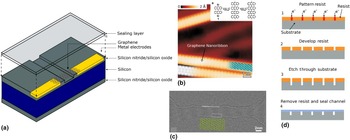
The last devices that will be discussed here consist of a GNR adjacent to a nanofluidic channel [Fig. 1(d)]. The proposed device works by detecting changes in the graphene current due to adsorption of DNA as it translates through the nanofluidic channel. A schematic of the proposed device geometry is shown in Fig. 4(a) with the envisioned devices consisting of a GNR bridging a nanofluidic channel on a SiNx (or SiO2) film. A sealing layer is placed over the nanochannel to enable fluid flow. These devices have been studied computationally where it was predicted that π − π stacking between nucleobases and a nanometer-wide graphene ribbon can lead to base-specific changes in the graphene current due to Fano resonances.[Reference Min, Kim, Cho and Kim27, Reference Cho, Min, Kim and Kim76] Fabrication of devices capable of measuring the current in a nanometer-wide graphene ribbon while DNA translates through an adjacent nanochannel is yet to be demonstrated.
(a) Schematic of the proposed device geometry. (b) Scanning tunnelling microscopy image of GNRs created via bottom-up synthesis. The inset shows the reaction scheme for the precursor monomers into GNRs.[Reference Cai, Ruffieux, Jaafar, Bieri, Braun, Blankenburg, Muoth, Seitsonen, Saleh, Feng, Mllen and Fasel73] (c) Transmission electron micrograph image of a GNR which has been sculpted using high-energy electrons produced in a TEM.[Reference Xu, Wu, Schneider, Houben, Malladi, Dekker, Yucelen, Dunin-Borkowski and Zandbergen74] (d) Schematic representation of the process to create nanofluidic channels in a substrate via electron beam lithography. Figures adapted with permissions from (b) Nature publishing group,[Reference Cai, Ruffieux, Jaafar, Bieri, Braun, Blankenburg, Muoth, Seitsonen, Saleh, Feng, Mllen and Fasel73] (c) American Chemical Society.[Reference Xu, Wu, Schneider, Houben, Malladi, Dekker, Yucelen, Dunin-Borkowski and Zandbergen74]

One of the major challenges in the fabrication of these devices is creating GNRs with widths on the order of 1 nm to ensure a limited number of nucleobases interact with the graphene at a given time. One technique to reliably create nanometer-wide graphene ribbons is via bottom-up synthesis. This method relies on the surface-assisted coupling of molecular precursors followed by their subsequent cyclodehydrogenation[Reference Cai, Ruffieux, Jaafar, Bieri, Braun, Blankenburg, Muoth, Seitsonen, Saleh, Feng, Mllen and Fasel73] [Fig. 4(b)]. The controlled alignment of these nanoribbons with electrodes and a nanofluidic channel is likely to be a challenge, however, this could potentially be overcome by developing self-alignment techniques such as dielectrophoretic deposition. Similar alignment issues may also be encountered with several other GNR fabrication techniques such as nanowire lithography[Reference Bai, Duan and Huang77] and unzipping of carbon nanotubes.[Reference Jiao, Zhang, Wang, Diankov and Dai78] GNRs with widths on the order of 20 nm have been fabricated via electron beam lithography,[Reference Han, zyilmaz, Zhang and Kim79] and their widths further reduced via gas-phase oxidation.[Reference Wang and Dai80] However, it is difficult to produce widths below 10 nm using this technique due to edge roughness introduced during electron beam lithography. Direct patterning of GNRs can also be achieved using energetic charged particles from a TEM[Reference Xu, Wu, Schneider, Houben, Malladi, Dekker, Yucelen, Dunin-Borkowski and Zandbergen74, Reference Fischbein and Drndić81] [Fig. 4(c)] or helium ion microscope.[Reference Bell, Lemme, Stern, Williams and Marcus82]
The fabrication of nanofluidic channels as well as DNA translocation through these channels have been described elsewhere.[Reference Xia, Yan and Hou83, Reference Duan, Wang and Xie84] Techniques such as electron beam lithography,[Reference Hibara, Saito, Kim, Tokeshi, Ooi, Nakao and Kitamori85–Reference Riehn, Austin and Sturm87] interferometric lithography,[Reference Xia, Ku, Lee and Brueck88] and nanoimprint lithography are commonly used to create nanofluidic channels.[Reference Guo, Cheng and Chou89–Reference Liang and Chou91] Briefly, these techniques generally involve patterning of a resist followed by etching of the substrate [shown in Fig. 4(d) for electron beam lithography]. These techniques create open nanofluidic channels that must be sealed to enable fluid flow. This can be done via, anodic bonding of a cover slide to the substrate. Metal electrodes may need to be patterned into the substrate to ensure a planar surface that allows for nanochannel sealing. This can be achieved by etching the substrate an appropriate thickness prior to metal deposition.[Reference Maleki, Mohammadi and Ziaie92] Note that further studies may need to be done to determine the channel dimensions required to ensure interaction between the DNA and graphene.
Finally, challenges in graphene transfer and contamination will be discussed. While this is clearly an important consideration for all the graphene-based sequencing techniques, it is discussed in this section as contamination may pose a significant issue for these devices as they rely on DNA adsorbing to graphene. Depending on the source of graphene, different graphene transfer methods may be used such as substrate etching, wedge transfer[Reference Schneider, Calado, Zandbergen, Vandersypen and Dekker93] and bubble transfer.[Reference Wang, Zheng, Xu, Dubuisson, Bao, Lu and Loh94] These techniques leave graphene suspended in an aqueous solution which can then be captured on the desired substrate. A polymeric film over the graphene is typically used during the transfer process to avoid the breaking of graphene. Graphene contamination may occur due to residues of this polymeric film, or other films introduced during lithographic steps. Such residues can be (partially) removed via current annealing[Reference Moser, Barreiro and Bachtold95] and thermal annealing.[Reference Ishigami, Chen, Cullen, Fuhrer and Williams96] Current and thermal annealing may also be used to remove atmospheric contamination on graphene, however, the surface will become quickly recontaminated when exposed to atmosphere. Techniques such as electrochemically cleaning graphene in solution have been studied and could potentially be used in situ to avoid graphene recontamination.[Reference Fu, Feng, Panaitov, Kireev, Mayer, Offenhusser and Krause97]
While the idea to sequence DNA using changes in the current through a GNR due to physisorption of DNA translating through an adjacent nanochannel was first suggested in 2011,[Reference Min, Kim, Cho and Kim27] there are yet to be any reports on the fabrication of these devices. This has likely been due to challenges in the fabrication of GNRs with widths on the order of 1 nm and their alignment with contact electrodes and a nanofluidic channel. Techniques such as dielectrophoretic deposition could potentially be used to align graphene and scalably produce devices, however, significant work will need to be done on the development of such techniques.
Conclusion and outlook
Graphene-based electronic DNA sequencing devices have received significant attention from the research community over the past decade. These devices are hoped to not only deliver on the advantages of ionic current nanopore sequencing, but also provide single base resolution, high bandwidth sampling, easy multiplexing and the potential for scalable manufacturing. In particular, three device designs have been suggested; (i) monitor the graphene current as DNA translates through a pore in the graphene, (ii) monitor the tunnelling current across a graphene nanogap as DNA translates through the gap and (iii) monitor the current through a GNR as DNA translates through an adjacent nanochannel. Despite the significant promise of these sequencing techniques, DNA sequencing using these devices is yet to be demonstrated. This has been partly due to the complex fabrication requirements of these devices resulting in low fabrication yields and limited throughput. Indeed, this will need to be addressed if DNA sequencing using these devices is to be realized. In particular, the development of robust, wafer-scale processes for substrate and electrode fabrication will be required. Additionally, techniques to scalably fabricate nanostructures in graphene, such as gaps and pores, as well as the alignment of these structures will need to be advanced. Given the relative infancy of graphene and the rapid development of nanofabrication techniques the authors are hopeful that such techniques will indeed by developed in the coming years. If this does indeed happen, it would represent a significant step toward graphene-based electronic DNA sequencing being realized.
Acknowledgments
This work was funded by the UK EPSRC (Grant No. EP/N017188/1). JAM is a RAEng Engineering for Development Research Fellow. JPF thanks the Oxford Australia Scholarship Fund for funding.