Introduction
The development of novel nonvolatile memories (NVMs) is key to further our ability to retain, share, and process the ever-growing amount of data generated every day. Current NVMs based on Flash technology suffer from relatively low speeds and limited endurance. Among the alternative options to Flash technology, phase-change memoriesReference Pirovano, Lacaita, Benvenuti, Pellizzer and Bez1,Reference Lacaita and Redaelli2 stand out as one of the most promising candidates, as attested to by the recent Optane memory, based on the Intel/Micron 3D Xpoint technology that entered the market in 2017 as a storage-class memory.Reference Choe3
In phase-change memories, information is encoded into two different phases of phase-change materials (PCMs) such as chalcogenide alloys,Reference Wuttig and Yamada4,Reference Lencer, Salinga and Wuttig5 which can reversibly (up to ∼1012 times)Reference Kim, BrightSky, Masuda, Sosa, Kim, Bruce, Carta, Fraczak, Cheng, Ray, Zhu, Lung, Suu and Lam6,Reference Kim, Kim and Nam7 switch between the crystalline and amorphous phases upon Joule heating within a few nanoseconds (see the article by Kim et al. in this issueReference Kim, Kim and Nam7). The two phases have markedly different electrical resistance values that are exploited in the memory readout.
Although the Ge2Sb2Te5 compound is presently the material of choice for phase-change memories, the quest for alloys with better performance continues.Reference Lencer, Salinga and Wuttig5,Reference Rao, Ding, Zhou, Zheng, Xia, Lv, Song, Feng, Ronneberger, Mazzarello, Zhang and Ma8 For embedded applications in the automotive industry, for instance, data retention above 100°C is desirable, which is not achievable with Ge2Sb2Te5. Other applications such as neuro-inspired computingReference Burr, Shelby, Sebastian, Kim, Kim, Sidler, Virwani, Ishii, Narayanan, Fumarola, Sanches, Boybat, Le Gallo, Moon, Woo, Hwang and Leblebici9 and photonic devicesReference Wuttig, Bhaskaran and Taubner10 would also benefit from tailoring of the functional properties of phase-change alloys. To this end, a thorough understanding of the microscopic features of PCMs is mandatory.
In this regard, atomistic simulations can provide valuable microscopic information that would be difficult to be gained experimentally. First-principles (or ab initio) electronic-structure calculations are usually the tool of the trade, and the field has greatly benefited from molecular dynamics (MD) simulations based on density functional theory (DFT).Reference Lencer, Salinga and Wuttig5,Reference Rao, Ding, Zhou, Zheng, Xia, Lv, Song, Feng, Ronneberger, Mazzarello, Zhang and Ma8,Reference Caravati, Bernasconi, Kühne, Krack and Parrinello11–Reference Zhang, Deringer, Dronskowski, Mazzarello, Ma and Wuttig14
Nonetheless, investigations of many properties of phase-change alloys lie well beyond the capabilities of DFT methods. For instance, the crystallization of amorphous nanowires (a possible alternative architecture for phase-change memories) requires simulations of ∼104 atoms for several nanoseconds, while DFT simulations are typically limited to a few hundred atoms for up to few nanoseconds.
For a well-studied material such as silicon, it is straightforward to perform large-scale simulations by picking an empirical/classical potential of choice and by striking some balance between accuracy (some of which would be lost) and computational efficiency. However, even though a classical interatomic potential has been devised for GeTe,Reference Zipoli and Curioni15 PCMs display complex interplay between different atomic environments,Reference Deringer, Dronskowski and Wuttig16 which makes the construction of classical potentials challenging.
One way to solve this conundrum, where DFT is not fast enough, and classical potentials are not accurate enough, is to harness machine learning (ML) algorithmsReference Behler17–Reference Jordan and Mitchell19 to build interatomic potentials with (quasi-) ab initio accuracy and a computational efficiency (almost) comparable to that of classical potentials.
ML-based interatomic potentials
ML is by now a pervasive aspect of technology that is percolating rapidly into many scientific fields. Materials science is no exception, as ML may very well deliver the next generation of interatomic potentials for atomistic simulations. Currently, in this field, ML algorithms are used as a flexible tool to build a potential energy surface by fitting a large data set (104–105 configurations) of DFT energies and forces of relatively small (102 atoms) configurations; two popular approaches in this context are based on Gaussian approximationsReference Bartók and Csányi20 and neural networks (NNs).Reference Behler and Parrinello21
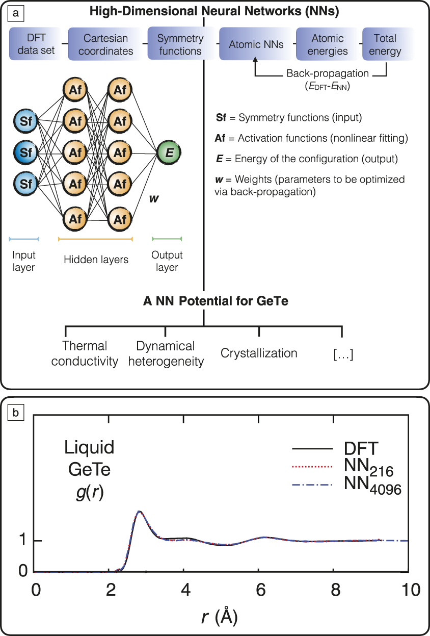
In the NN method of Behler and Parrinello,Reference Behler and Parrinello21 the total energy of the system is written as the sum of atomic energies and the structure of the system is encoded by means of so-called symmetry functions that describe the local atomic environment of each atom up to a cutoff radius typically encompassing up to the third coordination shell. As depicted in Figure 1a, the symmetry functions represent the input of a feed-forward NN, which consists of a collection of nodes and layers where the inputs are subject to a nonlinear transformation (via so-called activation functions) and then are linearly combined via a number of “weights” to eventually yield the total energy of a given configuration. The weights are randomly initialized and then refined by back-propagation in order to minimize the mismatch between the energies predicted by the NN and by DFT.Reference Behler and Parrinello21,Reference Behler22 Once a sufficiently good fitting is achieved, we can leverage it to obtain the energy of large models at low computational cost that scales linearly with the number of atoms. Crucially, forces and stress are readily available from NN potentials, thus enabling fast MD simulations while retaining an accuracy close to that of the underlying DFT calculations.
(a) Neural networks (NNs) can be harnessed to construct a machine learning-based interatomic potential starting from a data set of density functional theory (DFT) energies of small (100 atoms) configurations. The weights, w, of the NN are assigned by back-propagation, which is a procedure aimed at minimizing the mismatch between the energy predicted by the NN (E NN) and the DFT energies (E DFT). (b) Total pair correlation function, g(r), of liquid GeTe from a NN simulation with 4096 and 216 atoms, compared with DFT results for the smaller cell. The g(r) gives a measure of the probability of finding an atom at a distance r from an atom set at the origin. Adapted with permission from Reference Reference Sosso, Miceli, Caravati, Behler and Bernasconi23. © 2012 American Physical Society.

In the next sections, we illustrate how the neural network potential (NNP) for the prototypical phase-change compound GeTe that was generated in 2012Reference Sosso, Miceli, Caravati, Behler and Bernasconi23 has allowed addressing several properties ranging from dynamical heterogeneity and fast crystallization in the liquid phase to structural relaxations in the amorphous phase.
Functional properties of the PCM GeTe
A NNP for GeTe
The NNP for GeTe described in References Reference Sosso, Miceli, Caravati, Behler and Bernasconi23 and Reference Gabardi, Baldi, Bosoni, Campi, Caravati, Sosso, Behler and Bernasconi24 was constructed from the DFT energies of ∼30,000 configurations containing 64 to 216 atoms. The potential was validated against DFT calculations (an example is illustrated in Figure 1b) and it is capable of describing the bulk phases of GeTe as well as surfaces, nanowires, and nanoparticles.
As a first application, the NNP was used to compute the thermal conductivity of the amorphous phaseReference Sosso, Donadio, Caravati, Behler and Bernasconi25 and the thermal-boundary resistance at the amorphous–crystalline interface.Reference Campi, Donadio, Sosso, Behler and Bernasconi26 On this topic, the reader is referred to a recent review on the thermal properties of amorphous materials studied by means of ML potentials.Reference Sosso, Deringer, Elliott and Csányi27
Fragility of supercooled liquid and structural relaxations in glass
In phase-change memories, crystallization of the amorphous phase is achieved by electrical pulses that bring the material to a supercooled liquid state above the glass-transition temperature, T g. One of the key properties of PCMs is that they tend to be fragile liquids,Reference Weber, Orava, Kaban, Pries and Greer28 which means that their viscosity (η) remains fairly low at large supercooling, only to rise sharply very close to T g. This feature allows atoms to remain highly mobile at low temperatures (T), albeit above T g, where the thermodynamical driving force for crystal nucleation and growth is also high.Reference Weber, Orava, Kaban, Pries and Greer28 The NNP developed in Reference Reference Sosso, Miceli, Caravati, Behler and Bernasconi23 allowedReference Sosso, Behler and Bernasconi29 the function η(T) to be computed, providing an estimate of the so-called fragility index (the slope of η(T) at T g), which turned out to be in reasonable agreement with later experimental data from ultrafast differential scanning calorimetry.Reference Weber, Orava, Kaban, Pries and Greer28
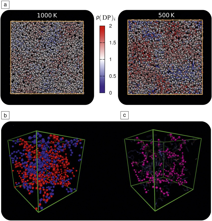
The atomic mobility at low T is further enhanced by a breakdown of the Stokes–Einstein relation between viscosity and diffusivity that was also predicted by MD simulations.Reference Sosso, Behler and Bernasconi29 This feature is typical of fragile liquids and is often ascribed to the emergence of dynamical heterogeneities consisting of spatially separated domains in which atoms move substantially faster or slower than average. This is illustrated in Figure 2a. Close to the melting temperature, the distinction between slow (blue) and fast (red) moving regions is minimal. However, as the system is cooled down, one can clearly notice the emergence of spatially localized domains (Figure 2b).Reference Sosso, Colombo, Behler, Del Gado and Bernasconi30 These results were obtained by the so-called isoconfigurational analysis technique, which involves a large number (∼100) of MD simulations.Reference Sosso, Colombo, Behler, Del Gado and Bernasconi30
Dynamical heterogeneity in liquid GeTe from molecular dynamics simulations employing a neural network potential. (a) The color map refers to the density ρ of the dynamical propensity (DP), calculated according to Equation 4 in Reference Reference Sosso, Colombo, Behler, Del Gado and Bernasconi30. Slow- and fast-moving domains are highlighted in blue and red, respectively. (b) Spatially localized clusters of slow- and fast-moving atoms at 500 K. Chains of Ge–Ge bonds found in most mobile regions (purple) are highlighted in (c). Adapted with permission from Reference Reference Sosso, Colombo, Behler, Del Gado and Bernasconi30. © 2014 American Physical Society.

Most notably, it turns out that fast-moving regions involve structural heterogeneities in the form of chains of Ge–Ge bonds, depicted in Figure 2c. These chains are ultimately responsible for the breakdown of the Stokes–Einstein relation and thus for an enhancement of atomic mobility at high supercooling, which boosts the crystallization speed. They also play a role in the so-called resistance drift–a practical issue for phase-change memories whereby the resistance of the amorphous phase increases over time due to aging. In fact, by combining NNP and DFT calculations, it was found that Ge–Ge chains are responsible for localized electronic states within the gap of the amorphous phase.Reference Gabardi, Caravati, Sosso, Behler and Bernasconi31 Removal of these chains via structural relaxations over time (aging) leads to an energy gain and to a widening of the bandgap,Reference Gabardi, Caravati, Sosso, Behler and Bernasconi31 which can explain the resistance drift (see Reference Reference Raty32 for a review).
Moreover, it was recently shown that the presence of Ge–Ge chains provides a rationale for the experimentally measured reduction of the resistance drift in GeTe nanowires,Reference Gabardi, Baldi, Bosoni, Campi, Caravati, Sosso, Behler and Bernasconi24 whose amorphous structure is characterized, on average, by a lower fraction of Ge–Ge chains compared to the bulk.
Crystal nucleation and growth
The short time scale of crystal nucleation and growth of PCMs offers the unique opportunity for DFT methods to study the crystallization process by means of unbiased MD simulations with an affordable computational load.Reference Sosso, Chen, Cox, Fitzner, Pedevilla, Zen and Michaelides33 Indeed, this has been achieved in several works,Reference Hegedüs and Elliott12,Reference Zhang, Mazzarello, Wuttig and Ma34 but the usage of still relatively small models inevitably leads to spurious interactions between the newborn crystalline nuclei and their periodic images, thus affecting both induction times and crystal growth velocities.
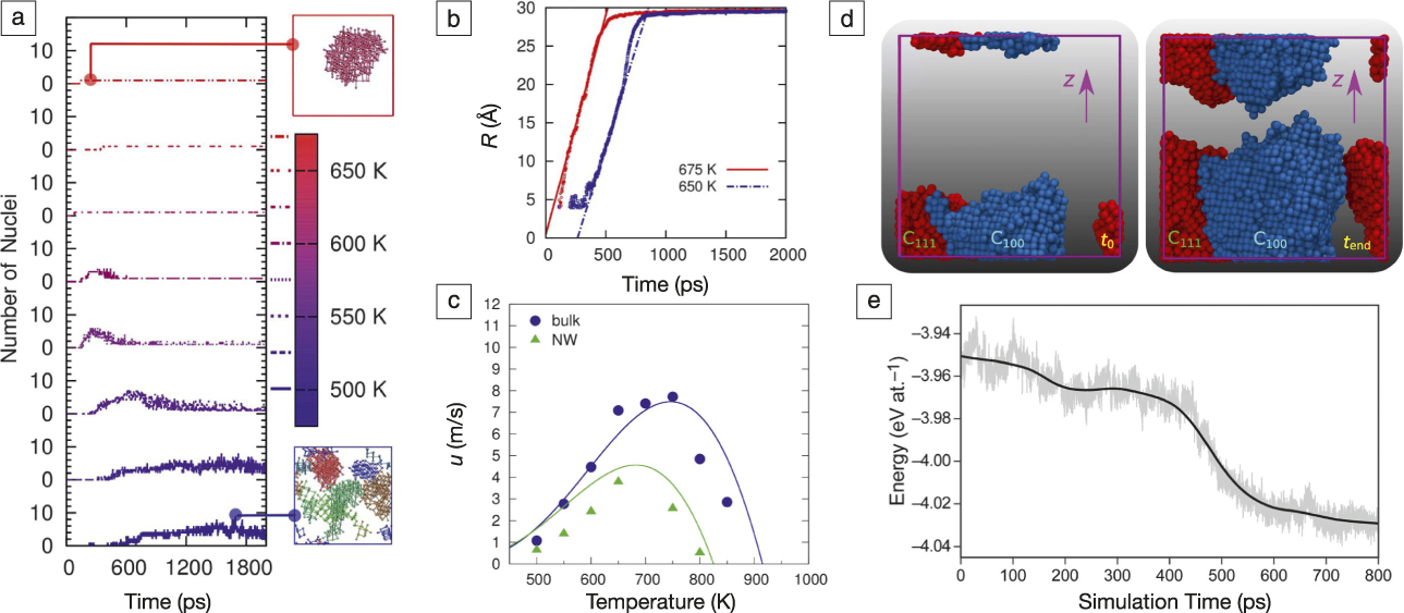
The advent of NNP was a game changer in this respect, as it allowed the extent of finite size effects to be assessed (they are avoidable by using supercells containing at least about 1000 atoms) and to investigate crystal nucleation and growth in a wide range of conditions for supercells containing 4000–32,000 atoms.Reference Sosso, Miceli, Caravati, Giberti, Behler and Bernasconi35–Reference Sosso, Salvalaglio, Behler, Bernasconi and Parrinello37 Some of these findings are summarized in Figure 3. It was possible to identify different nucleation regimes at different temperatures (Figure 3a) and to accurately estimate the crystal growth velocity, extracted from the slope of growth profiles (Figure 3b). Recently, these growth rates were compared with those obtained for GeTe nanowiresReference Gabardi, Baldi, Bosoni, Campi, Caravati, Sosso, Behler and Bernasconi24 (Figure 3c), which enabled the study of the effects of nanostructuring on crystallization kinetics.
(a–d) Results on the crystallization of GeTe from molecular dynamics simulations using a neural network potential. (a) Number of crystalline nuclei (>29 atoms) at different temperatures as a function of time in supercooled liquid GeTe. The number of nuclei first increases and then decreases due to coalescence. The two snapshots (insets at the top and bottom) show crystalline atoms forming a single nucleus or several nuclei at high and low temperatures, respectively. (b) The radius, R, of a crystalline nucleus of GeTe at two temperatures as a function of time. Reprinted with permission from Reference Reference Sosso, Miceli, Caravati, Giberti, Behler and Bernasconi35. © 2013 American Chemical Society. (c) Crystal growth velocity, u, of a GeTe nanowire (NW, green triangles) and at the crystal/liquid interface in the bulk (blue circles). Reprinted with permission from Reference Reference Gabardi, Baldi, Bosoni, Campi, Caravati, Sosso, Behler and Bernasconi24. © 2017 American Chemical Society. (d) C111 (red) and C100 (blue) crystalline grains in a polycrystalline model of GeTe at the beginning (t 0) and end (t end) of the simulation. Projections along the xz planes are shown. Reprinted with permission from Reference Reference Sosso, Salvalaglio, Behler, Bernasconi and Parrinello37. © 2015 American Chemical Society. (e) Potential energy as a function of time in the simulation of the crystallization of Ge2Sb2Te5 with a Gaussian approximation potential. Reprinted with permission from Reference Reference Mocanu, Csányi and Elliott38. © 2018 American Chemical Society.

Heterogeneous growth of crystalline GeTe,Reference Sosso, Salvalaglio, Behler, Bernasconi and Parrinello37 a scenario of utmost relevance for phase-change memories, was also addressed by using large models of polycrystalline GeTe that allowed the competition between the growth of different grains to be followed (Figure 3d). Moreover, simulations of the crystallization of the most studied ternary compound Ge2Sb2Te5 have been performed recently by means of a ML-based interatomic potentialReference Mocanu, Csányi and Elliott38 based on Gaussian approximations (the so-called GAP approachReference Bartók and Csányi20): A representative result is reported in Figure 3e.
Conclusions
Although DFT simulations have provided invaluable contributions to the study of PCMs, there is the need to bring MD simulations closer to the size scale of real memories in order to address key issues for the improvement of devices. ML-based interatomic potentials represent an effective solution, in that they can overcome the limitations of DFT calculations in terms of size and simulation time while keeping a quasi-ab initio accuracy.
In this article, we have illustrated some of the results obtained by means of a NNP for GeTe. The methodologies needed to construct ML potentials are now more accessible than they were in 2012 when the GeTe potential was devised. While a substantial effort is still needed to collect the huge data set of DFT energies, several promising advances,Reference Chan, Narayanan, Cherukara, Sen, Sasikumar, Gray, Chan and Sankaranarayanan39,Reference Zhang, Lin, Wang and Car40 including stratifiedReference Hajinazar, Shao and Kolmogorov41 and implantedReference Onat, Cubuk, Malone and Kaxiras42 NN are now available to tackle multicomponent alloys.Reference Kobayashi, Giofré, Junge, Ceriotti and Curtin43
There remain open questions in the field of phase-change memories that would greatly benefit from large-scale simulations of multicomponent alloys such as the switching mechanism of Ge-rich alloys for automotive applicationsReference Palumbo, Zuliani, Borghi and Annunziata44 and of superlattices/interfacial phase-change memories.Reference Simpson, Fons, Kolobov, Fukaya, Krbal, Yagi and Tominaga45 For the hotly debated switching mechanism of interfacial phase-change memories,Reference Boniardi, Boschker, Momand, Kooi, Redaelli and Calarco46 DFT simulations have provided a number of different scenarios among which large-scale simulations might ultimately be able to identify the most plausible one. The impact of confinement effects and nanostructuring on crystallization kinetics is another issue where ML potentials can make a difference. Our previous work on GeTe nanowires is an example, but much remains to be explored, such as the fascinating possibility of monoatomic phase-change memoriesReference Salinga, Kersting, Ronneberger, Jonnalagadda, Vu, Le Gallo, Giannopoulos, Cojocaru-Mirédin, Mazzarello and Sebastian47 or PCMs encapsulated in carbon nanotubes,Reference Wynn, Medeiros, Vasylenko, Sloan, Quigley and Morris48 or even as isolated nanoparticles.Reference Chen, ten Brink, Palasantzas and Kooi49
Besides the generation of interatomic potentials, ML and in particular NNs, have been recently exploited to predict glass properties by learning from the existing experimental database.Reference Cassar, de Carvalho and Zanotto50–Reference Onbaşlı, Tandia, Mauro, Andreoni and Yip54 There are still relatively few examples of this type of application of ML in glass science, and none so far for tellurides of interest for phase-change memories. However, the field is rapidly evolving and the growth of available data on phase-change alloys from both experiments and MD simulations could trigger the harnessing of ML to optimize alloy composition for tailored applications.
In conclusion, in light of what the community has achieved in the last few years, we feel that ML can truly contribute to the rational design of PCMs for memories and other applications in the near future.
Acknowledgments
We acknowledge the contributions of several co-workers and, in particular, of J. Behler, who introduced us to the use of NN methods.

Gabriele C. Sosso is an assistant professor of computational physical chemistry at the University of Warwick, UK. He earned his MS degree in materials science in 2009, and his PhD degree in nanostructures and nanotechnologies in 2013 from the University of Milano-Bicocca, Italy. He completed postdoctoral research at ETH Zürich, Switzerland, and at University College London, UK. His research interests include disordered systems and phase transitions, focusing on crystal nucleation and growth. Sosso can be reached by email at g.sosso@warwick.ac.uk.

Marco Bernasconi is a full professor of theoretical condensed-matter physics and dean of the Doctorate School in Materials Science and Nanotechnology at the University of Milano-Bicocca, Italy. He received his PhD degree in physics from Sissa-Trieste in 1993. After several years at the Max-Planck-Institut, Germany, he moved to Milano-Bicocca in 1998. His research focuses on electronic-structure calculations and molecular dynamics simulations of materials for applications in microelectronics and photonics. Bernasconi can be reached by email at marco.bernasconi@unimib.it.