I. INTRODUCTION
With the rapid progress in the wireless communications, there is an increased demand for antenna solutions that provide wide band, small size, low cost, and high performance. For ultra-wide band (UWB) antennas in particular, the necessity to offer high performance over a very wide bandwidth joint with small size presents a number of key antenna design challenges [Reference Kearney, John and Ammann1–Reference See, Abd-Alhameed, Zhou and Excell4]. An UWB antenna is defined by the federal communication commission (FCC) as a device with a fractional bandwidth greater than 0.25 or occupies a spectrum of 1.5 GHz or more, while the frequency band for commercial communication is between 3.1 and 10.6 GHz [5]. In recent years, there have been a number of antenna designs using different techniques to achieve UWB operations, including the use of different shapes such as a V-shaped [Reference Elsadek and Nashaat6], a circular shape [Reference Liang, Chiau, Chen and Parini7], a rectangular-shaped antenna with slots on the patch and steps [Reference Choi, Park, Kim and Park8], a rectangular shape with slits on the ground plane [Reference Shagar and Wahidabanu9], or fractal shaped [Reference Ghatak, Ghoshal, Mondal and Bhattacharjee10].
In this paper, we propose a planar inverted-F antenna (PIFA) that is a successful candidate for most mobile phone application [Reference Abedin and Ali11–Reference Chang and Wong13] and laptop computers [Reference Lee and Wong14]. So far, the PIFA has generally been considered as a narrow band antenna, but a lot of effort has been made to broaden its bandwidth including the use of parasitic element [Reference Chattha, Huang, Lu and Zhu15–Reference Virga and Rahmat-Samii17], adding a slot [Reference Zuazola, Batchelor, Elmirghani and Gomes18] or using a capacitive feed [Reference Wu and Wong19].
The objective of this study is to demonstrate a very effective method of bandwidth enhancement for PIFA. It was done by adding a J-shaped slot and a parasitic element.
The UWB PIFA studied in this paper has a rectangular-radiating plate with a J-shaped slot and a parasitic element. The paper is organized as follows. In Section II, the major elements of the proposed antenna are described. In Section III, details of the proposed antenna design and simulated results are presented and discussed. In Section IV, a parametric study is made for different PIFA parameters. The conclusions are drawn in the last section.
The software package used for simulation is Ansoft's high-frequency structure simulator, which is based on the finite-element method. The obtained results of our developed antenna was a bandwidth of 7.8 GHz for S11 < −10 dB from 2.9 to 10.7 GHz, which can cover the UWB application.
II. ANTENNA CONFIGURATION
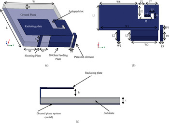
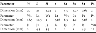
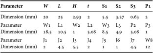
Figure 1 depicts the geometry of the proposed UWB PIFA, and more detailed dimensions are given in Table 1. The ground plane has dimensions of W × L, whereas the radiating plate with an irregular shape has dimensions of W1 × L1 and the thickness of the copper used is 0.15 mm. The antenna height is h and the space between the radiating plate and the ground plane is filled with air. The material used is FR4 substrate with a dielectric constant of 4.4, a tangent loss of 0.02 and a substrate height of 2 mm. The shorting plate's dimensions are W2 × L2, the feeding plate's dimensions are W3 × L3, and the distance between the radiating plate and the parasitic element is S3. It should also be noted that the antenna is fed by a 50 Ω microstrip line. To design the UWB antenna, we have applied two techniques to the proposed antenna: the use of (1) a parasitic element and (2) a J-shaped slot on the radiating plate. By selecting these parameters, the proposed antenna can be tuned to operate in the 2.9–10.7 GHz range. The antenna achieves a very wide bandwidth, smaller ground plane, and radiating plate size than the design reported in other papers. For example, a study done by Abutarboush et al. [Reference Abutarboush, Nilavalan, Peter and Cheung12] reports a volume of the proposed UWB antenna of 40 × 40 × 3.57 mm3, while a volume of 30 × 15 × 4, 30 × 11.5 × 1.9, and 42 × 50 × 1.9 mm3 was reported by See et al. [Reference See, Abd-Alhameed, Zhou and Excell4], S. H. Choi et al. [Reference Choi, Park, Kim and Park8], and J. Liang et al. [Reference Liang, Chiau, Chen and Parini7], respectively. Whereas the overall volume of our studied UWB PIFA including the ground plane is only 20 × 25 × 5.08 mm3.
The layout of the proposed antenna: (a) 3D view, (b) detailed dimensions, and (c) profile view.

Detailed dimensions of the proposed antenna.
II. RESULTS AND DISCUSSION
A) Reflection coefficient S11
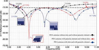
Figure 2 shows the effect of the slots and the parasitic element on the reflection coefficient of the proposed antenna by three curves. The first curve shows the reflection coefficient of the proposed antenna without a slot and a parasitic element, the conventional PIFA resonates in the vicinity of 3.5 GHz. In this case, the result shows a 4.86 GHz bandwidth under −10 dB reflection coefficient requirement. On the second curve, the bandwidth becomes wider by locating a parasitic element, which makes an additional resonant point in the upper frequency around 8.5 GHz. Finally, another resonant point is caused by adding slots to the radiating plate. As shown in Fig. 2, the bandwidth achieved by a PIFA with slots and a parasitic element for S11 < −10 dB is 7.8 GHz, from about 2.9 to 10.7 GHz. This result confirms the UWB characteristic of the proposed PIFA.
The simulated reflection coefficient S11 in dB versus frequency in GHz.

B) Input impedance and current distribution
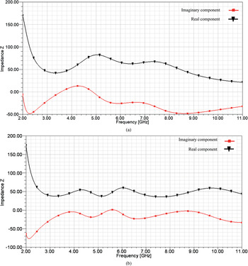
As shown in Fig. 3, the real and imaginary components of the input impedance do not change too significantly and thus remains around 50 and 0 Ω, respectively, all over the UWB (2.9–10.7 GHz).
The input impedance Z in Ω versus frequency in GHz for the studied PIFA (a) The PIFA antenna without slot and without parasitic element (b) The proposed UWB PIFA antenna.

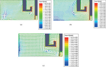
The simulated surface current distributions at different frequencies for the proposed UWB PIFA are presented in Fig. 4. Figure 4(a) shows the current pattern at 3 GHz. The current pattern at 6 GHz is given in Fig. 4(b). Figure 4(c) illustrates the current pattern at 9 GHz, corresponding approximately to the third resonance. It can be seen that the current is distributed almost all over the surface of the PIFA. On the other hand, we notice that the maximum current distribution is close to the slot and decreases away from it, and the current path follows the curvature of the J slot in the three studied frequencies.
The simulated surface current distributions for the studied PIFA: (a) f = 3 GHz, (b) f = 6 GHz, and (c) f = 9 GHz.

C) Radiation patterns
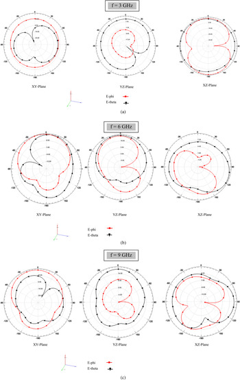
The simulated two-dimensional (2D) radiation patterns of the conventional PIFA without slots and a parasitic element at 3, 6 and 9 GHz are presented in Fig. 5 (a)–(c), respectively.
The simulated 2D radiation patterns for the PIFA without slot and without parasitic element at (a) 3 GHz, (b) 6 GHz, and (c) 9 GHz.

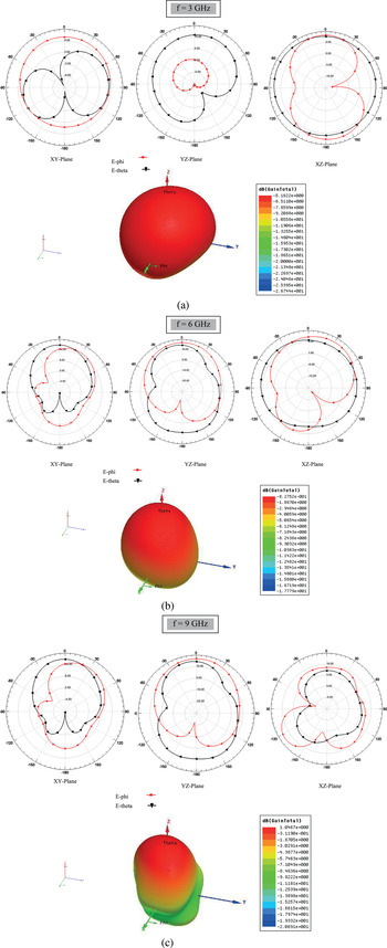
The simulated 2D and 3D radiation patterns for the proposed UWB PIFA at 3, 6, and 9 GHz are plotted in Fig. 6. The 2D patterns represent the E-phi and the E-theta components separately, while the 3D radiation patterns show the total radiation power, as seen the patterns are almost omni-directional. In general, no nulls are observed in the total-power radiation patterns, which is required for UWB applications [Reference Powell20].
The simulated 2D and 3D radiation patterns at (a) 3 GHz, (b) 6 GHz, and (c) 9GHz for the proposed UWB PIFA.

IV. PARAMETRIC STUDIES
A parametric study was performed to understand the reflection coefficient variation of the proposed antenna by modifying the parameter values. Five parameters were selected for this work, the ground plane length, the ground plane width, the ground plane thickness, the antenna height, and the parasitic element position. These parameters are considered crucial in determining the lowest and the highest frequencies of the operating bandwidth. The procedure adopted for this study is to change only one parameter at a time and observe its effects, whereas the other parameters are held constant.
A) Ground plane effect
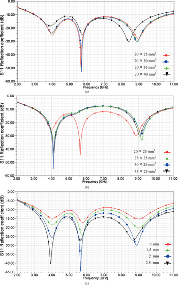
The ground plane of a PIFA can play an important role in enhancing the performance of the antenna [Reference Ghatak, Ghoshal, Mondal and Bhattacharjee10]. The designation of ground plane concerns the system ground plane (metal) together with the FR4 substrate. In this section, we study the effects of different ground plane dimensions as shown in Fig. 7. For this reason, we change only one parameter at a time and observe its effects on the reflection coefficient while all other parameters are held constant. Different sets of parameters are simulated to cover a wide range of values. For convenience, a ground plane reference is chosen with the parameters shown in Table 1. Figure 7(a) illustrates the effect of the ground plane length on the reflection coefficient of the studied PIFA. We observe that the length of the ground plane does not affect the resonance frequency except for 40 mm, whereas the effect of the ground plane width is given in Fig. 7(b), we can see that by changing the width of the ground plane we lose the second resonance frequency which is the frequency added by slots. Finally, Fig. 7(c) shows the effects of the ground plane thickness on the reflection coefficient of the studied antenna, we note that the impedance bandwidth increases with an increase in the thickness of the substrate.
The simulated reflection coefficient S11 in dB versus frequency in GHz for different values of ground plane: (a) length, (b) width, and (c) thickness.

B) Height of the PIFA
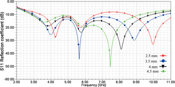
Figure 8 shows the effects of the height h of the UWB PIFA above the ground plane on the reflection coefficient. Two observations were made. First, the resonance frequency decreases with an increase in the height of the antenna, and second, increasing the height of the antenna increases the bandwidth [Reference Ibnyaich, Elbakouchi, Ghammaz and Hassani21].
The simulated reflection coefficient S11 in dB versus frequency in GHz for different values of the height of the antenna.

We conclude that the height of the antenna also has strong effects on the antenna reflection.
C) Parasitic element location
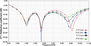
The location of the parasitic element strongly affects the performance of the studied UWB antenna. However, Fig. 9 shows that by changing just a few millimeters S3 the distance between the PIFA and the parasitic element, we obtain certain modifications on the reflection coefficient only for high frequencies greater than 8.5 GHz.
The simulated reflection coefficient S11 in dB versus frequency in GHz for different values of S3.

V. CONCLUSION
This study has focused on the development of UWB PIFAs. It has been shown that by adding a J-shaped slot and a parasitic element to the studied PIFA, we obtain an antenna that covers the UWB frequency band from 2.9 to 10.7 GHz. Simulation results have revealed good performances in terms of reflection coefficient, radiation pattern, impedance, and current distribution.
 Saida Ibnyaich was born in Morocco, in 1979. She received the Bachelor of sciences (4 years study after the baccalaureate) in electronic engineering from Cadi Ayyad University, Marrakesh Morocco, in 2002. She has also received the DESA (equivalent to M.A.) in Electrical Engineering, Power Electronics and Industrial Control from Cadi Ayyad University; Marrakesh Morocco, in 2005. She is currently working toward the Ph.D. degree at the Department of Physics, Electronics and Instrumentation Laboratory, Cadi Ayyad University of Marrakesh, Morocco. Her research interest includes telecommunications and antennas.
 Abdelilah Ghammaz received the Doctor of Electronic degree from the National Polytechnic Institut (ENSEEIHT) of Toulouse, France, in 1993. In 1994, he went back to University Cadi Ayyad of Marrakech – Morroco. Since 2003, he has been a Professor at the Faculty of Sciences and Technology, Marrakech, Morroco. His research interests are in the field of electromagnetic compatibility and antennas.
 Moha M'rabet Hassani was born in Morocco, in 1954. He received the Third Cycle Doctorate in automatic and signal processing from The University of Nice, France, in 1982, and the Ph.D. degree in electrical engineering from the University of Sherbrooke, Canada, in 1992. He joined Cadi Ayyad University, Marrakesh, Morocco, in 1982 as an Assistant Professor. Since 1993, he has been a Professor at the Faculty of Sciences Semlalia, Marrakesh, Morocco. His research interests are mainly nonlinear process modeling and identification applied to telecommunication and solar energy fields.