Introduction
In recent years, due to the development of wireless communication techniques, there is a huge demand for power portable and embedded devices such as mobile phones, RFID, etc. There is also wide research going on for replacing the chemical batteries in powering devices with harvesting techniques to make it eco-friendly. One such harvesting technique is wireless power transfer (WPT) [Reference Visser and Vullers1]. The basic block diagram of the receiving end of the WPT system mainly consists of an RF source (receiving antenna) matched to the rectifier using an impedance matching network. The obtained DC power from the rectifier can be used to power various low power applications such as sensors. In the WPT application, the design of the high gain antenna plays an important role. Patch antenna with high gain can be obtained using different techniques such as parasitic patches, aperture coupling, and stacked patches. Though these techniques increase the gain of the antenna, they also make the antenna bulky. Hence, to increase the gain of patch antenna without making it bulky and to improve the ease of fabrication, electromagnetic bandgap structures (EBGs) have been proposed by Sievenpiper [Reference Sievenpiper, Lijun, Broas, Alexopolous and Yablonovitch2].
EBGs are a type of high impedance structure and can be modeled as an LC parallel resonator circuit. They are arranged periodically either on the substrate or ground plane to form an artificial substrate or artificial ground. Surface waves are generated due to the mismatch of dielectric constants of substrate and air in the substrate. The surface waves add destructively with the outward propagating waves resulting in degradation of the performance of the antenna. Thus EBGs designed around the antenna act as stopband filters for the surface waves which suppressthe surface waves in the substrate and therefore enhance the performance of the antenna [Reference Yang and Rahmat-Samii3, Reference Sravya and Kumari4] in terms of gain or bandwidth. Mushroom EBGs (MEBG) are the most commonly used EBG as they have high stopband bandwidth and are more compact than the other two-dimensional EBG designs [Reference Sravya and Kumari4]. Gain enhancement of 2 dB is achieved for a circular patch using a cylindrical MEBG [Reference Boutayeb and Denidni5]. For a two-element aperture coupled patch antenna, using MEBG placed at the edge of the substrate, a gain enhancement of 4 dB is obtained [Reference McKinzie, Nair, Thrasher, Smith, Hughes and Parisi6]. Optimizing the position of MEBG for an inset fed patch antenna, the gain of the antenna is enhanced from 1.5 to 3 dB [Reference Neo and Lee7]. In [Reference Malekpoor and Jam8], using MEBG the gain of CPW-fed four-element array has been enhanced to 4.5 dB from 2 dB at 6.8 GHz and to 7 dB from 6 dB at 9.5 GHz. It can be observed that using MEBG, the gain of the antenna at one particular frequency is improved whereas enhancing gain at multiple frequencies is difficult. To address this drawback of MEBG, cascading of EBGs has been proposed in [Reference Liang, Liang, Zhao and Su9–Reference Shi and Jiang11]. EBGs can be modeled as LC parallel resonator circuit, so cascading of EBGs is similar to that of cascading bandstop filters. As discussed in [Reference Liang, Liang, Zhao and Su9–Reference Shi and Jiang11], by changing either patch width or vias radius or periodicity of MEBG, cascaded EBGs can be obtained.
A detailed discussion on antenna design is presented in section “Antenna design” which is followed by the rectenna design in section “Wireless power transfer application”. The fabricated results of the proposed antenna are explained in section “Experimental results” and the paper is concluded with a brief conclusion in section “Conclusion”. All simulations are done in HFSS. v. 15. This is an extension of the work presented in IEEE MTT-S International Microwave Workshop Series on Advanced Materials and Processes for RF and THz Applications (IMWS-AMP) [Reference Sravya, Kumari and Choudhury12].
Antenna design
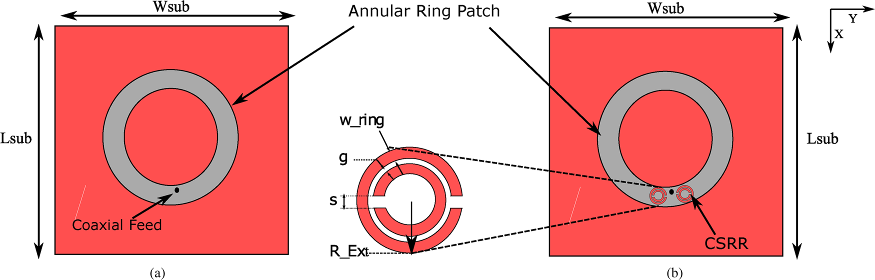
Annular ring patch antenna or ring patch antenna (ARP) being more compact and having better gain than rectangular and circular patch antennas, it is one of the most used antenna designs for various applications. In the proposed work, ARP with coaxial feed for 6.8 GHz is designed on a low-cost FR-4 substrate of dielectric constant, ɛr = 4.4, loss tangent 0.02, and thickness 1.6 mm. The feed is at an offset of 14 and 2 mm along X and Y -directions respectively. The antenna resonates at 6.8 GHz with 6 dB of gain and 267 MHz of bandwidth (design A) as shown in Fig. 1(a). It has been observed that ARP provides a narrow bandwidth. Thus, an attempt has been made to increase the bandwidth for the antenna using a complementary split-ring resonator (CSRR) (design B) as shown in Fig. 1(b).
Schematic of (a) design A and (b) design B.

ARP with CSRR
CSRR is a resonant structure that can resonate at two different frequencies. Two CSRR rings are placed near feed and are etched from the patch. When CSRR is etched from the patch, the antenna resonates at multiple frequencies apart from the fundamental resonance of the patch and hence increases the bandwidth of the antenna. The CSRRs are placed at a distance g left and g right from the feed which is optimized by a parametric study.
Parametric analysis of ARP with only left CSRR
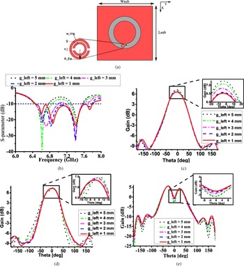
The S-parameter for different g left is shown in Fig. 2(a). It can be seen that for g left = 5, 4, and 3 mm; the fundamental resonance of ARP is shifted to 6.6 GHz from 6.8 GHz without any change in the bandwidth of ARP. Though an additional resonance at 7.4 GHz is obtained, the gain is very low. When g left is 2 or 1 mm, the ARP resonates at three resonance frequencies, 6.4, 6.8, and 7.4 GHz. It can also be observed that the bandwidth increased to 1.3 GHz for both g left = 2 and 1 mm. In Figs 2(c)–2(e) the 2D radiation patterns are plotted for various g left at 6. 4, 6.8, and 7.4 GHz. For all offset positions, the gains at 6.8 and 6.4 GHz are almost the same. But at 7.4 GHz, the maximum obtained gain is for g left = 1 mm. Hence, the left CSRR position is optimized to offset 1 mm from the feed to obtain maximum bandwidth of 1.3 GHz and maximum gains of 6.4, 7.3, and − 0.3 dB at the resonance frequencies.
(a) Schematic of design A with only left CSRR. Parametric analysis of ARP with only left CSRR. (b) S-parameter. (c) 2D radiation patterns at 6.8 GHz. (d) 2D radiation patterns at 6.4 GHz. (e) 2D radiation patterns at 7.4 GHz.

Parametric analysis of ARP with only right CSRR
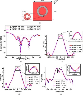
The S-parameter for different g right is shown in Fig. 3(a). For g right = 0.5 and 1 mm, ARP resonates at three frequencies with a total bandwidth of 900 MHz. However, for other values of g right, no bandwidth enhancement is observed. At g right = 0.5 mm, the antenna resonated at 6.4, 6.8, and 7.4 GHz with gains 6.8, 6.8, and 0.2 dB respectively. Hence, the right CSRR position is optimized to offset 0.5 mm from the feed to obtain maximum bandwidth of 900 MHz and maximum gain of 6.8, 6.8, and 0.2 dB at the resonance frequencies.
(a) Schematic of design A with only right CSRR. Parametric analysis of ARP with only right CSRR. (b) S-parameter. (c) 2D radiation patterns at 6.8 GHz. (d) 2D radiation patterns at 6.4 GHz. (e) 2D radiation patterns at 7.4 GHz.

From the parametric analysis, it is observed that using only left CSRR, the bandwidth of ARP is enhanced but the gain at 7.4 GHz is low (− 0.3 dB). Whereas when only right CSRR is used the bandwidth enhances up to 900 MHz with 0.2 dB of gain at 7.4 GHz which is the best gain achieved among all the offset positions. Therefore, by introducing both CSRRs, bandwidth, and gain of ARP at the resonance frequencies can be enhanced.
ARP with two CSRR and cascaded EBG
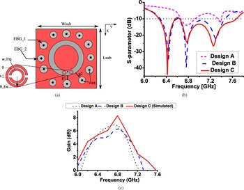
ARP with two CSRR resonates at 6.4, 6.8, and 7.4 GHz with impedance bandwidth of 17% (design B) as shown in Fig. 4(b). However, the gain at 7.4 GHz is very low. To enhance the gain of the antenna, EBGs are used in the proposed work. EBGs are similar to bandstop filters which suppress the flow of electromagnetic fields in a specific band of frequencies. When EBGs are designed on the substrate and placed around the patch, they suppress the surface waves in the substrate which will enhance the performance of patch antenna in terms of either gain or bandwidth. The standard square MEBG is modified into circular MEBG with circular symmetry as it occupies a lesser area than that of standard MEBG.
(a) Annular ring patch antenna with cascaded EBGs (antenna design C). (b) S-parameters of designs A, B, and C. (c) Gain versus frequency of design A, B, and C.

One layer of circular MEBG of radius 5 mm is designed and placed around ARP at distance, g 1. It is observed that for g 1 = 1 mm, gain at 6.8 GHz is enhanced to 8.3 dB from 7.3 dB without affecting the gains at 6.4 and 7.4 GHz. Furthermore, when the EBG layer designed with a 3 mm radius circular MEBG is placed around ARP at distance, g 2 = 5 mm, the gain at 7.4 GHz is increased to 2 dB from 0.2 dB. The proposed EBG with radii 5 and 3 mm has the resonant frequencies at 6.8 and 7.4 GHz with a stopband bandwidth range of 400 MHz (6.5–6.9 GHz) and 300 MHz (7.3–7.6 GHz). Since the resonant frequency is beyond the stopband bandwidth range of both the EBG, the gain of the antenna at 6.4 GHz is unchanged.
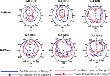
Hence, the cascading of EBG layers is used to increase the gain of ARP at two frequencies (design C). The schematic of the proposed antenna, its S-parameter, and the gain versus frequency is shown in Fig. 4. Although there is no change in the reflection coefficient and resonance after the introduction of EBGs around the patch with CSRR, a gain improvement at 6.8 and 7.4 GHz, and a 100 MHz of bandwidth enhancement are achieved. The normalized radiation patterns of both E and H-planes at 6.8, 6.4, and 7.4 are provided in Fig. 5. It can be observed that due to the introduction of the EBGs, the cross-polarization at 6.8 and 7.4 GHz frequencies is reduced which indicates an increase in the gain at those frequencies.
Normalized E-plane radiation patterns of design B and C at (a) 6.8 GHz, (b) 6.4 GHz, (c) 7.4 GHz. Normalized H-plane radiation patterns of design B and C at (d) 6.8 GHz, (e) 6.4 GHz, (f) 7.4 GHz.

Wireless power transfer application
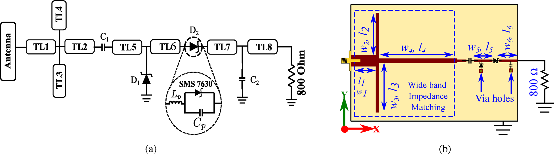
Previous works report different variations of the rectifier topologies such as half-wave rectifier [Reference Pinuela, Mitcheson and Lucyszyn13, Reference Sun, Guo, He and Zhong14], voltage doubler topology [Reference Georgiadis, Vera Andia and Collado15, Reference Arrawatia, Baghini and Kumar16], Greinacher topology [Reference Song, Huang, Zhou, Zhang, Yuan and Carter17, Reference Olgun, Chen and Volakis18]. Rectifier circuit integrated with an antenna designed at 6.8 GHz for WPT application has not been explored in published literature. Thus, in this work, an attempt has been made to analyze the performance of the rectifier circuit for an antenna with an aim to implement a broadband rectifying circuit covering the three frequencies 6.4, 6.8, and 7.2 GHz. Among the other rectifier circuit topologies, here voltage doubler is chosen as it gives a better output voltage and is less complex than that of half-wave and Greinacher rectifier topology respectively. Therefore, a voltage doubler rectifier is designed that covers all the three frequencies at which the antenna exhibits a good reflection coefficient and decent gain. The schematic is shown in Fig. 6 for a wide band rectifier design. The diodes, D 1 and D 2 used are SMS 7630-079LF from Skyworks (USA) and the capacitors, C 1 and C 2, each 100 pF are GCM series capacitors from Murata (USA). The main parameter to characterize the usability of the circuit for power transfer is the power conversion efficiency (PCE), which is the ratio of the output DC power obtained across the load to that of the input RF power received by the rectifier from the antenna.

(a) Rectifier circuit schematic with Schottky diode package parasitics Lp = 0.7 nH, Cp = 0.16 pF. (b) Rectifier prototype schematic with dimensions (in mm): w1 = 3, w2 = 0.96, w3 = 0.96, w4 = 1.54, w5 = 0.7, w6 = 0.7, l1 = 4.38, l2 = 12.34, l3 = 12.34, l4 = 19.3, l5 = 4.5, l6 = 4.5.

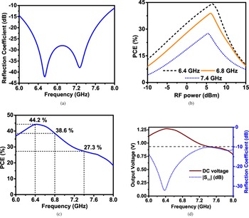
The rectifier proposed is designed on a low-cost FR4 substrate (ɛrr = 4 : 4, tan γ = 0 : 02) of thickness 1.6 mm. The rectenna simulations are done in Keysight ADS using the Harmonic Balance (HB), Large Signal S-parameter (LSSP) simulators and it is carried out in two phases. In phase I, the rectifier circuit consisting of capacitors and diodes without a matching network is simulated to find out the input impedances at a constant input power. This simulation gives the load for maximum possible efficiency at each of the frequencies of operation along with the input impedance of the entire circuit. The final load impedance of the rectifier is fixed at 800 Ohms so that all the three frequencies of operation are covered in the rectifier circuit. A wide band impedance matching network is designed and optimized in Keysight ADS to cover the entire frequency range from 6 to 8 GHz as shown in Fig. 7(a), since the frequencies on interest lie in this range.
(a) Response of the wide band impedance matching network. (b) RVariation of PCE with RF power at 6.4, 6.8, and 7.4 GHz. (c) Variation of PCE with frequency. (d) Output DC voltage and reflection coefficient of the complete rectifier with varying frequency.

In the second phase, the voltage doubler topology is matched to the RF source (antenna) through double-sided open-end stubs. To replicate the antenna impedance, the S-parameters of the antenna are imported into ADS using a Data Access Component (DAC). Figure 7(b) shows the PCE variation with input RF power for the three frequencies. The maximum value is obtained as 44.2% at 6.4 GHz for an input power of 6.5 dBm. At the frequency of 6.8 GHz, the observed value is 38.6% at 6 dBm input power. Similarly, at the third frequency of interest at 7.2 GHz, the PCE is 27.3% at 5.4 dBm. In order to further verify the obtained values, the PCE is now plotted with varying frequency in Fig. 7(c) and similar PCE values are obtained, thereby validating the results obtained in Fig. 7(b). In Fig. 7(d), the output DC voltage is plotted across the frequency range, and it is seen that the corresponding DC voltages at 6.4, 6.8, and 7.4 GHz are 1.27, 1.17, and 0.94 V, respectively. The same graph also shows the variation of the reflection coefficient of the overall rectifier circuit. An important inference from this study is, as the frequency of operation of rectifier increased from 6.4 to 7.4 GHz, the PCE has reduced from 44.3 to 27.8%, as seen from Fig. 7(b). Similar variation is found with the DC voltage observed across the output load as plotted in Fig. 7(d). Thus, a single rectifier with a wide impedance matching network is designed to operate along with the antenna for the WPT application.
Experimental results
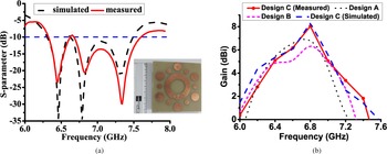
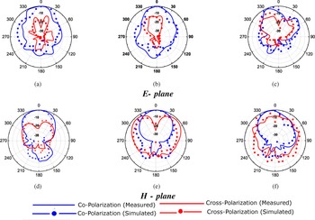
The prototype of the proposed antenna, ARP with CSRR, and cascaded EBG is fabricated and tested as shown in Fig. 8(a). The measured and the simulated results of the proposed antenna, shown in Fig. 8, indicate that the resonance frequencies and bandwidth measured are similar to the simulated results obtained though there is a slight reduction in the magnitude of |S 11|. The measured gain of the proposed antenna, design C is compared with that of simulated results of design A, B, and C as shown in Fig. 8(b). It is observed that the gain at the 6.8 and 7.4 GHz frequencies is enhanced by 1.2 and 2 dB using multi-cell EBG without any change on the gain at 6.4 GHz. The normalized E-plane and H-plane radiation patterns of fabricated antenna compared with the simualted results are shown in Fig. 9.
(a) Measured and simulated |S 11| of design C. (b) Gain versus frequency for design A, B, and C.

Normalized radiation patterns of antenna design C at (a) 6.8 GHz, (b) 6.4 GHz, and (c) 7.4 GHz.

Conclusion
In this paper, a ring patch antenna for RF energy harvesting application is proposed. The bandwidth of the annular ring patch antenna is increased from 267 MHz to 1.2 GHz by etching out two CSRRs from a patch near the feed. Parametric analysis on the effect of the CSRR offset from the feed is done and the optimum position for both left and right CSRRs is chosen. The proposed ring patch resonates at 6.4, 6.8, and 7.4 GHz with an impedance bandwidth of 17% and gains 6.8, 6.8, and 0.2 dB respectively. Cascaded circular MEBG with circular symmetry is designed on the substrate to enhance the gains at 6.8 and 7.4 GHz to 8.5 and 2 dB respectively. Due to the suppression of surface waves in the substrate by cascaded EBG, an additional 100 MHz bandwidth enhancement is also achieved. The results of the antenna integrated with the rectifier circuit designed at 6.8 GHz are also presented. The overall structure obtained a maximum simulated PCE of 40% and DC output voltage of 1.2 V for 7 dBm input power. This rectenna can be integrated with a power management circuit for sensors applications.
 Sravya R. Venkata obtained BTech in electronics and communication engineering from Jawaharlal Nehru Technological University, Hyderabad, Telangana, India, in 2014, and the MDes degree in communication engineering from Indian Institute of Information Technology, Design and Manufacturing, Chennai, Tamil Nadu, India, in 2016. She is currently a research scholar with the Department of Electrical and Electronics Engineering, Birla Institute of Technology & Science, Pilani, Hyderabad campus, India, pursuing her PhD. Her current research areas are electromagnetic bandgap structures and metamaterials design.
 Vinnakota Sarath Sankar completed Ph.D. from the Department of Electrical and Electronics Engineering, Birla Institute of Technology & Science, Pilani, Hyderabad campus, India. His current research areas are rectenna designs for wireless energy harvesting & wireless power transfer, metasurface antennas, and microwave circuit design.
 Runa Kumari obtained BE and MTech from Biju Patnaik University of Technology, Odisha, in 2003 and 2008, respectively, and earned a PhD from the National Institute of Technology, Rourkela, India, in 2014. Currently she is working as an associate professor at the Department of Electrical and Electronics Engineering, Birla Institute of Technology & Science, Pilani, Hyderabad campus. Her current research interests include log periodic antenna, dielectric resonator antenna, planar antenna, reconfigurable planar antennas, and metamaterial. Kumari is a senior member of IEEE.