I. INTRODUCTION
Doped polysilicon (poly-Si) films have long been integral to various Si electronic devices as interlayers between active device layers and metal contacts, and have contributed to high gain in bipolar junction transistors by lowering the base current and emitter resistance.Reference Van Halen and Pulfrey1 In these structures, the presence of an intermediate tunneling SiOx layer <2 nm between the poly-Si and the single crystal silicon wafer advantageously provides wafer surface passivation without the degradation of transport.Reference Green, Gusev, Degraeve and Garfunkel2 Shallow emitters are formed by diffusing dopants from the poly-Si through the SiOx into the wafer via post deposition anneals.Reference Gan3 This must be carefully optimized due to possible detrimental side effects such as oxide break-up, secondary phase formation due to heavy doping, and blistering. Advantageously, dopants tend to segregate along grain boundaries and pile-up at the poly-Si/SiOx interface. This has been shown to increase passivation by lowering carrier mobility along grain boundaries in the former, and to chemically bond to dangling bonds in the latter.Reference Post, Ashburn and Wolstenholme4
When doped poly-Si films on SiOx stacks are applied to solar cells, they form p-n or high-low junctions. These exhibit excellent surface passivation of the wafer by the SiOx interlayer and low contact resistance enabled by leakage/tunneling current through the SiOx layer from the doped poly-Si. Since the heavily doped poly-Si is separated from the wafer by the SiOx, there is no need for additional surface passivation (as in conventional Si cells, e.g., by SiNx), and the metal contacts can be applied directly to poly-Si. Therefore, poly-Si films on SiOx contacts to Si wafer provide a close to ideal scenario to create the necessary carrier collecting junctions with selective carrier extraction and to mitigate metallization degradation. This has resulted in very high efficiency cells (>25%) that are process temperature tolerant.Reference Glunz, Feldmann, Richter, Bivour, Reichel, Steinkemper, Benick and Hermle5 Traditionally, poly-Si has been deposited via low pressure or atmospheric pressure chemical vapor deposition at temperatures over 550 °C; however, this results in double sided deposition with a wrap-around problem. Single-side approaches offer the flexibility of additive processes, without the need for film removal.
Our target cell structures are shown in Fig. 1. Our primary structure is a “hybrid” architecture [Fig. 1(a)] where the back surface field (BSF) of the cell is a full area passivated contact, and the front is a ∼130 Ω/□ (Ohms per square) thermally diffused B-emitter passivated by an Al2O3/SiNx stack. The alternative structure [Fig. 1(b)] is fully based on tunneling passivated contact structures both as emitter and BSF.
Desired cell structures with n+ poly-Si on SiOx passivated contact BSF coupled with: a) thermally diffused B-emitter, and b) p+ poly-Si on SiOx passivated contact emitter.

We report a low-temperature, single-sided plasma enhanced chemical vapor deposition (PECVD) route to deposit doped a-Si:H on tunneling SiOx and then anneal to form poly-Si on SiOx passivated contact stacks. Furthermore, we introduce a novel passivation technique to improve the passivated contact performance. We investigate the effect of the individual layer properties (tunneling oxide and poly-Si) on the performance of the passivated contacts, and their interaction during the cell process. Finally, we address the mechanisms responsible for the observed contact degradation by their metallization, and demonstrate ways to minimize it.
II. EXPERIMENTAL
Figure 2 shows the passivated contact test structures used in this study. We initially grow a tunneling SiOx layer on silicon wafers either chemically or thermally, and then deposit doped a-Si:H at low temperature via PECVD on each side to create a final symmetric structure, which is annealed at high temperature to solid-phase crystallize (SPC) the resulting poly-Si.
Consecutive steps of symmetric passivated contact sample formation.
A. Tunneling SiOx formation
Norsun (Oslo, Norway) phosphorus doped n-type Cz (n-Cz) Si wafers (conductivity 4 Ω cm) with both pyramid-textured and KOH saw-damage-removed (SDR) surfaces, Topsil (Frederikssun, Denmark) boron doped p-type FZ (p-FZ) wafers (2 Ω cm) double-side polished, and intrinsic wafers were RCA (Radio Corporation of America) cleaned (Standard Clean [SC] including both SC-1 [organic and particle clean, basic] and SC-2 [ionic clean, acidic]), and then subjected to thin (∼1.5 nm as verified by ellipsometry) SiOx growth either chemically, via room temperature HNO3 [NAOS (Ref. Reference Asuha, Maida, Takahashi and Iwasa6)] or thermally, as a low temperature oxide [LTO (Refs. Reference van der Meulen7 and Reference Fehlner8)] in a quartz tube furnace with a 6:1 N2/O2 mixture at around 700 °C.
B. Amorphous silicon deposition and crystallization
All a-Si:H layers were grown in a parallel plate configuration via 13.56 MHz PECVD in a multichamber cluster tool manufactured by MVSystems, Inc. (Arvada, Colorado) at a substrate temperature of approximately 350 °C and chamber pressure 1.0 Torr. The heavily doped amorphous silicon (a-Si:H) was deposited on both sides of a wafer sample to produce a symmetric structure using a H2 to SiH4 flow ratio of R = 50, along with appropriate doping gases B2H6 (2.6% dilute in H2) or PH3 (3% dilute in H2) for desired films. Witness films were also deposited on cleaned quartz slides. The a-Si:H was thermally SPC into poly-Si in a tube furnace with N2 flow at 850 °C for various durations. It should be noted that the adhesion of as-grown a-Si:H as well as crystallized poly-Si to SiOx depends on the H2/SiH4 ratio as well as the SiOx preparation. This is discussed further in following sections.
C. Passivation/metallization
Samples were subjected to a forming gas anneal (FGA) at 450 °C, and were further passivated with an atomic layer deposited (ALD) Al2O3 film grown in a Beneq reactor (Espoo, Finland) using trimethylaluminum and H2O precursors at 200 °C. Samples were then annealed in a tube furnace with N2 flow at 400 °C for 20 min. The Al2O3 layer was removed via HF dip. Lastly, an additional PECVD grown doped a-Si:H film identical to the doped a-Si:H precursor previously described was deposited on the poly-Si as a metal diffusion barrier capping layer. These surfaces were metallized using e-beam Al deposited at 30 Å/s through patterned shadow masks. It is interesting to note that unlike traditional Al2O3 approaches applied to cell surfaces,Reference Dingemans and Kessels9 our Al2O3 is applied to the poly-Si as a sacrificial hydrogen source and is intended to be removed after hydrogen delivery to the passivated contact.
D. Characterization
Lifetime measurements were performed with a Sinton WCT-120 Lifetime tester (Boulder, Colorado) in the generalized (1/1) mode in high-level injection (Δn > 5 × 1015 cm−3) to extract implied open circuit (iVoc) values. Transport was measured using transmission line measurement (TLM) patterns 300 µm long spaced 500, 1000, 1500, and 2000 µm intervals with 1 µm thick evaporated Al pads. Hall measurements were made on quartz witness samples with pressed In contacts. Photoluminescence (PL) mapping was performed using an in-house 810 nm laser diode source and Si CMOS camera with a user defined exposure time. Film thicknesses were measured by an n&k Analyzer (San Jose, California) as well as an ellipsometer (JA Woolam alpha-SE, Lincoln, Nebraska), while scanning electron microscopy (SEM) images were acquired using a FEI Quanta 600 (Hillsboro, Oregon). In-house secondary ion mass spectrometry (SIMS) depth profiles were attained using 1.5 keV ion bombardment energy using an O2+ source.
III. RESULTS
A. Device
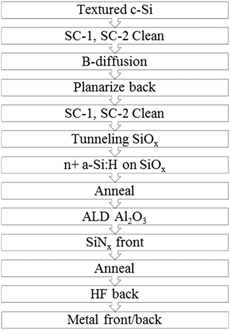
Our B-diffused emitter device [Fig. 1(a)] process follows the process sequence shown in Fig. 3. We ensure that exposed wafer surfaces are cleaned (SC-1 and SC-2) to preserve bulk lifetimes during dopant diffusion and oxidation. A key step relies on the nature of the ALD Al2O3 deposition, where all surfaces receive film growth. Since this is a requirement for our B-emitter surface passivation stack, we find the resulting hydrogenation of the bulk n+ poly-Si and interfaces of the passivated contact stack to be a serendipitous byproduct. Thus, Al2O3 passivates both the front (field effect and atomic hydrogen) and back (atomic hydrogen only) of the cell.
Process flow for B-diffused emitter and n+ poly-Si passivated back contact n-Cz cell.
While developing our own in-house B-diffusion process, we applied our n+ poly-Si passivated contact to a boron diffused emitter fabricated on a textured n-FZ wafer provided by the silicon research group at Fraunhofer ISE. It can be seen from the photoluminescence image in Fig. 4 that several of the n-FZ cells did not survive metallization; however, the best 2 × 2 cm2 cell efficiency measured was 21.5% with 693 mV, 39.6 mA/cm2, and 78.4% FF.Reference Stradins, Essig, Nemeth, Lee, Young, Norman, Liu, Luo, Warren, Dameron and LaSalvia10 After our own B-emitter process was developed (with Tabula Rasa pretreatment to suppress oxygen precipitation) on n-Cz wafers, device structures with an n+ poly-Si back passivated contact resulted in premetallized 724 mV iVoc after full passivation.Reference Nemeth, LaSalvia, Page, Warren, Dameron, Norman, Lee, Young and Stradins11 However, also in the n-Cz sample we see a similar degradation in PL intensity after metallization. These results prompted an ongoing study to determine a reliable method to metallize these contacts.
PL images of B-diffused emitter with n+ poly-Si back surface field before and after metallization on n-FZ (a,b) and n-Cz (c,d). Note exposure time for (a,b) is 1/1.3 sec, while (c,d) is 1/15 sec.
B. n-Type poly-Si passivated contact
1. Crystallization and dopant diffusion
We have determined that the n+ poly-Si passivated contact was sensitive to the metallization process and that the passivation quality is highly correlated with crystallization annealing conditions. Figure 5 shows SIMS depth profiles of the contact layers in the “As-Grown” state and after 5, 30, and 90 min anneals at 850 °C. It should be noted that primary beam collisional mixing will drive dopants and impurities deeper into the film and distort the profiles. However, we mitigated this by taking profiles with low ion-bombardment energies (1.5 keV O2+ ions). We have determined that these beam conditions give nearly identical SIMS profiles to those taken from the wafer side of the contact (after thinning the wafer to couple microns).
SIMS profiles for a) Phosphorus in the n+ poly-Si / thermal SiOx passivated contact annealed for various times at 850°C on cSi, and b) Hydrogen and Phosphorus in the 30 min, 850°C annealed n+ poly-Si / thermal SiOx passivated contact on cSi.
Dopants diffuse from the poly-Si through the thermal SiOx layer into the wafer with increasing anneal time. In addition, dopant pile-up at either the poly-Si/SiOx or SiOx/cSi interface can be seen in Fig. 5. This so-called snowplow effectReference Minamisawa, Papadopoulos, Jabrany, Knoll, Corvasce and Rahimo12 has been measured at interfaces with and without a SiOx interlayer and even when monolayer delta doping growths have been implemented.Reference Akazawa13 The effect is associated with chemical passivation of interfacial dangling bonds by dopant atoms. Peroxy linkage defects (PLDs) act as a low energy bridge for dopants to diffuse through the SiOx layer and become incorporated. The diffusivity of dopants is higher at the interface and strongly increases with decreasing oxide thicknesses below 80 Å due to the formation energy of PLD being lower at the Si/SiOx interface than in the SiOx bulk.Reference Fair14
2. Hydrogen-mediated passivation of the passivated contact by Al2O3 and SiNx
After crystallization, the contact stack is further passivated by reintroducing atomic hydrogen via FGA (Ref. Reference Reed and Plummer15) and/or ALD Al2O3 deposition and activation. Similarly, we have determined that SiNx:H (Refs. Reference Pollack, Richardson, Malhi, Bonifield, Shichijo, Banerjee, Elahy, Shah, Womack and Chatterjee16 and Reference Ok, Upadhyaya, Rounsaville, Madini, Jones, Ryu, Chandrasekaran, Das, McPherson, Gupta and Rohatgi17) films and subsequent anneals produce the same effect, whereas others utilize remote H plasma anneals.Reference Lindekugel, Lautenschlager, Ruof and Reber18Table I shows iVoc data for n+ poly-Si on SiOx symmetric stacks that have been passivated by either SiNx/FGA or Al2O3/N2 annealing treatments. We find that the excellent passivation largely remains even after Al2O3 is removed by an HF dip; however, we were unable to etch the SiNx effectively after thermal activation. Therefore, Al2O3 likely acts as a hydrogen reservoirReference Dingemans, Beyer, Van de Sanden and Kessels19 rather than as a field effect passivant to the stack. The mobile atomic H from the Al2O3 layer passivates grain boundaries, SiOx dangling bonds, and the critical wafer/SiOx interface.Reference Mihailetchi, Komatsu and Geerligs20–Reference Brotherton22Figure 5(b) shows SIMS depth profiles for n-type passivated layer stacks showing traces of P and H after an HF dip to remove the Al2O3 following the passivation anneal. Note that the hydrogen does not pile-up at the SiOx interfaces (unlike P), indicating a lower defect density at this location.
Hydrogenation of n+ poly-Si on SiOx passivated contact with SiNx and Al2O3.
To summarize how the passivation quality of the contacts evolves with each process step, Fig. 6 shows iVoc data from lifetime measurements performed on n+ poly-Si contact stacks throughout the contact formation process flow. n+ poly-Si samples are grown on n-Cz SDR wafers with (a) thermal SiOx (LTO) and (b) chemical SiOx (NAOS). The samples, referenced to the as-grown initial n+ a-Si:H on SiOx stack (black X), are crystallized and annealed in forming gas (FGA) (red crosses), passivated with Al2O3 (black circles), stripped with HF (green squares), and finally capped with the aforementioned intermediate n+ a-Si:H layer (blue triangles). For LTO samples [Fig. 6(a)], the passivation of the n-type contact decreases with increasing annealing time. This might be related to enhanced Auger recombination in the shallow doped region resulting from increased phosphorus diffusion into the wafer with anneal time [see Fig. 5(a)]. For NAOS SiOx [Fig. 6(b)], the n-type contact improves with annealing time. However, it never reaches the excellent initial passivation state of the n-type contact with LTO SiOx. We attribute this trend to the less dense nature of the NAOS SiOx compared with the LTO SiOx, and the longer annealing times help to densify the NAOS SiOx as well as diffuse phosphorus deeper into the wafer, resulting in an increase in final passivation.
Lifetime measurement of symmetric n+ poly-Si / SiOx on n-Cz SDR samples: As Grown, Crystallized and FGA, Al2O3 passivated, HF dipped, and n+ a-Si:H capped a) thermal SiOx (LTO) and b) chemical SiOx (NAOS).
For both samples, a distinct increase in passivation is seen once the Al2O3 treatment is performed, suggesting that its role is to provide atomic H to passivate dangling bonds (as mentioned previously) or to catalyze the healing of defects, rather than provide field-effect passivation. More recently, our group utilized this scheme to simultaneously passivate the back contact and emitter regions in an interdigitated back passivated contact cell structure.Reference Young, Nemeth, LaSalvia, Reedy, Essig, Bateman and Stradins23 We see that a small drop in iVoc occurs after the HF dip for the LTO sample; however, a drastic reduction in iVoc (∼100 mV) occurs for the chemical NAOS SiOx samples. The a-Si:H capping layer tends to heal this degradation to some degree, but the highest passivation is never fully recovered. Several factors can account for this reduction after the Al2O3 layer removal that relate to the density of the two different types of SiOx layers studied and resulting different blister formation to be discussed later.
C. p-Type poly-Si passivated contact
1. Crystallization and dopant diffusion
Figure 7 shows that boron diffuses from the poly-Si through the thermal SiOx layer into the wafer with increasing anneal time and piles-up at either the poly-Si/SiOx or SiOx/cSi interface. As-grown p+ poly-Si films have an order of magnitude of higher dopant concentration than n+ poly-Si films (Fig. 5). However, this does not lead to a significantly higher diffused dopant concentration into the cSi wafer after annealing, implying an additional diffusion mediating effect from the SiOx and slower diffusion of boron. Figure 7(b) shows SIMS depth profiles for the p-type passivated layer stacks showing traces of boron and hydrogen. The hydrogen appears to track with the boron profile and piles-up at the SiOx layer. Hydrogen tends to bind to crystallographic defects and dangling bonds, so this may indicate a more defective p-type contact compared with the n-type contact in Fig. 5.
SIMS profiles for a) Boron in the p+ poly-Si / thermal SiOx passivated contact annealed for various times at 850°C on cSi, and b) Hydrogen and Boron in the 30 min, 850°C annealed p+ poly-Si / thermal LTO SiOx passivated contact on cSi.
2. Hydrogen passivation by Al2O3
We have investigated the passivation quality of p+ poly-Si contacts both on n-Cz wafers (p-n junction) and on p-FZ wafers (high-low junction for BSF). Figure 8 shows iVoc data from lifetime measurements performed on p+ poly-Si contact stacks throughout the contact formation process flow on both thermal (LTO) and chemical (NAOS) SiOx (gray open squares) on (a) polished p-FZ wafers and (b) textured n-Cz wafers. The samples are crystallized and passivated with Al2O3 (black circles), stripped with HF (green squares), and finally capped with the precursor p+ a-Si:H layer (blue triangles). For LTO samples, the p-type contact initially increases in passivation quality with annealing time and saturates with further annealing. The explanation for this tendency may lie in Fig. 7, where we showed that H tends to track the B concentration throughout the contact stack. Presumably, annealing for longer times reduces defects in the stack, which are further passivated by subsequent atomic H treatment, but balanced by the increased boron diffusion into the wafer. We see that a small drop in iVoc again occurs after the HF dip for p-type contacts for LTO samples. This is more pronounced with the n-Cz sample. A significant difference is found for the fully passivated contact on chemical (NAOS) SiOx samples in Figs. 8(a) and 8(b), when compared to LTO samples, again likely due to density, surface chemistry differences, and resulting blistering.
Lifetime measurement of symmetric p+ poly-Si / thermal SiOx (LTO) on n-Cz SDR samples: Crystallized and Al2O3 passivated, HF dipped, and p+ a-Si:H capped compared with p+ poly-Si / chemical SiOx (NAOS) a) on polished p-FZ wafers (high-low junction) and b) on n-Cz textured wafers (p-n junction).
D. Transport properties of n+ and p+ passivated contacts
To test the electrical character of the contact, contact resistivity measurements were performed using a TLM contact pattern which was isolated by reactive ion etching after metallization. Figure 9 shows the results of these tests for n+ poly-Si and p+ poly-Si contacts with and without the a-Si:H capping layers on n-Cz and p-FZ, respectively. All stacks give a contact resistivity of <100 mΩ cm2 with all of the 90 min annealed samples showing less than 60 mΩ cm2. These are acceptable values for 1-sun Si solar cell full area contacts. The low resistivity values of the p+ poly-Si contacts (solid blue squares) may be due to metal diffusion through the SiOx layer. Fortunately, the addition of the a-Si:H capping layer does not increase the contact resistivity significantly, while preserving the passivation of the contact. Fortuitously, the n+ poly-Si contact resistivity improves with the addition of the a-Si:H capping layer for all annealing times. The additional dopants in the a-Si:H capping layer may help the metal to form a lower resistivity contact to the slightly depleted P surface of the n+ poly-Si contact.
Contact resistance measurements of poly-Si on LTO SiOx passivated contacts with and without a-Si:H interlayers. (Circles: n+ poly-Si on n-Cz, Squares: p+ poly-Si on p-FZ, Open: with additional a-Si:H capping layer).
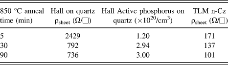
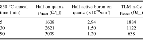
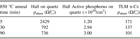
Tables II and III show ρsheet and dopant concentrations of both n+ and p+ poly-Si witness films on quartz via Hall effect measurements, contrasted with TLM ρsheet results of the same films on LTO SiOx/n-Cz wafers prior to isolation. Note that in the case of n+ poly-Si forming a high-low junction to n-Cz wafer, the TLM ρsheet includes the bulk wafer, whereas for p+ poly-Si contact on n-Cz wafer, the formed p-n junction prevents a current path into the wafer. A decrease in ρsheet with anneal time is likely due to increased dopant diffusion into the wafer for both samples, effectively forming a high-low junction from the poly-Si through the SiOx to the newly formed shallow emitter. The Hall measurements showed 1–3 × 10²⁰ active dopants (both P and B) for poly-Si films on quartz, with a decrease in active B and an increase in active P with anneal time.
n+ poly-Si passivated contact transport measurements on various substrates.
p+ poly-Si passivated contact transport measurements on various substrates.
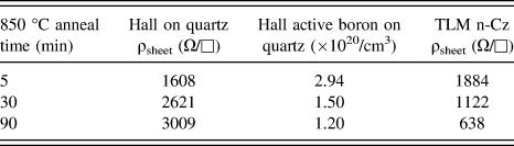
Understanding and optimizing the development of high performing p+ poly-Si on SiOx emitter contacts are critical to achieving our all-poly-Si cell approach in Fig. 1(b). The deactivation of boron with p+ poly-Si crystallization time on quartz in Table III can be explained by diffusion into the quartz substrate, secondary crystalline phase (SiBx) formation,Reference Abbasi and Brunnschweiler24 or complexing in the bulk via amorphous clustering.Reference Shao, Liu, Chen and Chu25,Reference Batra, Manning, Dennison, Sultan, Bhattacharya, Banerjee, Lobo, Lux, Kirschbaum, Norberg, Smith and Mulvaney26 However, B-deactivation is also seen when a similar anneal time comparison is performed on quartz samples with and without a SiNx B-diffusion barrier (Fig. 10). Secondary phase formation/complexing is therefore likely in the bulk of the p+ poly-Si or in the pile-up region when applied to tunneling SiOx on Si during crystallization. The Hall measurements on quartz indicate active dopant concentrations at least an order of magnitude lower than the total concentration of B as measured by SIMS. The p+ poly-Si films have a high amount of B, and once the solubility limitReference Kurachi and Yoshioka27 of B in Si is reached and a second phase (SiBx or boron rich layer) is formed, the B diffusivity is degraded.Reference Chen, Lei, Lin, Chang, Hsieh and Chen28 Since dopants will be segregated, it is likely that the SiBx phase will form at grain boundaries and interfaces.Reference Kanaki, Zianni and Narducci29
Decreasing active Boron concentration with crystallization time on p+ poly-Si on SiOx with and without SiNx diffusion barrier interlayer.
E. Metallization
1. Blisters and surface features
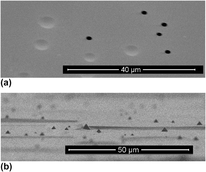
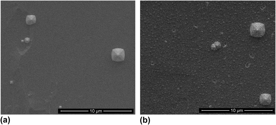
Though the passivation quality of these contact stacks are excellent up to the passivation annealing process step, subsequent metallization of the poly-Si layers can degrade their passivation quality. Metal deposition technique, purity of deposited metals, film blisters, poly-Si pinholes, or other metal diffusion paths can adversely affect the passivation quality. Figure 11(a) shows a plan-view SEM image of both ruptured and unruptured blisters formed in the p+ poly-Si contact stack after the crystallization anneal of a nonoptimized p+ poly-Si film on LTO SiOx. The blisters are likely formed from effusion of H2 and/or H2O coalescing at poly-Si/tunneling oxide interface and structural defects. Ruptured blisters provide a diffusion path for metals to degrade the passivation quality of the contact stack. These blisters can form during deposition or crystallization if growth and annealing conditions are not carefully optimized. Notably, B-doped films effuse hydrogen at lower temperatures than P-doped films,Reference Street30 and B-doped samples tend to have more severe blistering than P-doped samples do. Another metal diffusion path can occur when poor wafer surface preparation allows microtipReference Campbell, Cooper, Dixon, Earwaker, Port and Schiffrin31 features to form on saw damage KOH etched Si wafer surfaces. These microtips can be seen in Fig. 11(b) as small black pyramids that are often coincident with lifetime degradation, and are caused by incomplete planarization of the surface of the wafer by KOH.
SEM images of a) blistering in p+ poly-Si on SiOx film stack on cSi, and b) residual wafer surface microtips after its planarization by KOH.
To block metal diffusion pathways due to blisters or microtip features, we employ a thin doped a-Si:H capping layer over the poly-Si layers prior to metallization as shown by the passivation data in Figs. 6 and 8. This conformal layer “fills in” blister openings and provides adequate protection to the sensitive interfaces from the metal deposition and diffusion. Additionally, post metallization anneals (PMAs) are typically applied to mitigate e-beam, x-ray, or sputtering deposition damage to the contact layers.Reference Auret and Mooney32,Reference Kuwano and Ashok33
2. Enhanced metal degradation
To illustrate these points, Fig. 12 shows a set of PL images (normalized to the same exposure time) for the crystallization time series for n+ poly-Si/LTO SiOx on n-Cz (samples a–c) and p+ poly-Si/LTO SiOx on p-FZ wafers (samples d–f). For a given sample, the first column of images shows no difference between adding an a-Si:H capping layer (approximately 5 nm doped a-Si:H) before metallization and not adding the capping layer. The second column of images shows a drastic decrease in PL intensity for the samples without the a-Si:H capping layer between the metal (e-beam deposited Al in this example) and the contact stack. However, even the sample areas with the a-Si:H capping layer show some decrease in PL intensity likely due to e-beam deposition damage. Finally, the PL intensity of the samples increases after the PMA at 400 °C as shown in the third column of images. For the n+ poly-Si samples the areas with a-Si:H capping layers show a PL intensity slightly less than premetallized samples, but those without the capping layer rebound significantly from the metallization damage. However, the recovery is not to the extent of those with the a-Si:H capping layer, and localized depassivated regions become more clear likely due to metal diffusion. The p+ poly-Si samples show significant depassivation of the uncapped regions after the PMA. Overall, the data of Fig. 12 reveal that the metal deposition damage can be healed by annealing to some degree and also that the n-type contact is much more robust to metallization than the p-type contact. Sample (f), the 5 min 850 °C p+ poly-Si sample, is “dark” throughout the process flow due to severe blistering. Figure 12 reveals that with careful processing and contact design, metallization does not significantly degrade the passivation quality of the poly-Si contact stack.
PL images of p+ and n+ poly-Si on SiOx (note crystallization time) stacks with half sample capped with a-Si:H, metallized with Al and post metallization anneal (PMA).
3. Surface morphology
As mentioned previously, several factors, including blister formation, can account for the iVoc drop after the Al2O3 layer removal that relate to the density of the SiOx layers. Figure 13 shows two plan-view SEM images revealing small blister formation in the poly-Si films grown on a chemical (NAOS) oxide [Fig. 13(b)], but not on the thermal (LTO) oxide layers [Fig. 13(a)]. The denser thermal SiOx maintains its volume and does not evolve gases during the crystallization anneal. The less dense NAOS SiOx may densify and evolve gases that create bubbles or blisters under the poly-Si layer. Removing the Al2O3 from the LTO poly-Si contact does not expose much of the bare wafer surface to air due to the low density of blisters. However, removing the Al2O3 from the NAOS poly-Si contact exposes much more of the wafer surface, which subsequently depassivates the surface under ambient conditions. This simple areal blister problem explains the drop in iVoc after the HF removal of the Al2O3 passivation layer as seen in Fig. 6. The larger pyramidal features in Fig. 13 are the microtips previously shown in Fig. 11.
SEM images of n+ poly-Si passivated contact on a) LTO SiOx and b) NAOS.
IV. CONCLUSIONS
We present poly-Si on tunneling SiOx layer stacks as effective passivated contacts to crystal silicon wafers forming high quality high-low and p-n junctions. These contacts achieve over 700 mV iVoc for both n+ poly-Si to n-Cz and p+ poly-Si to p-FZ wafers, with contact resistivities below 100 mΩ cm2. The initial SiOx character largely governs the performance of the contact, where a denser, more stoichiometric oxide is desirable and is more resistant to defects such as blistering and delamination during deposition and in subsequent process steps. The poly-Si is crystallized from PECVD-grown phosphorus or boron doped a-Si:H films, and annealing time changes the diffusion profile of dopants from the poly-Si layer through the SiOx into the c-Si wafer. High temperature, thermal SiOx is dense and close to SiO2 stoichiometry, has few bulk defects, and provides excellent wafer surface chemical passivation. In contrast, chemically grown SiOx layers are usually less dense and off-stoichiometric, and often result in inferior passivation and blistering. Hydrogenation of the passivated contact stack is effectively achieved by annealing ALD grown Al2O3 thin films, which are then removed for contact metallization. After chemical removal of the alumina layer, the contact structures remain highly passivated by atomic hydrogen supplied by the alumina. Metallization decreases contact passivation both by inherent process externalities as well as by metal diffusion paths present in the poly-Si/SiOx stack such as film blistering. This can be mitigated by utilizing a thin a-Si:H interlayer and/or annealing.
ACKNOWLEDGMENTS
We would like to thank the silicon group at Fraunhofer ISE for providing n-FZ B-emitter samples, Ajeet Rohatgi at Georgia Tech for discussions, Adam Payne at Suniva for providing wafer random pyramid texturing, and Clay DeHart for aluminum e-beam deposition on samples. This work was supported by the U.S. Department of Energy EERE SETP under contracts DOE DE-EE00025783 and DE‐EE0006336.