Introduction
The current impact of today’s technology is that Internet of Things (IoT) ambient for body-worn applications in flexible, thin, and transparent sensors has numerous advantages and tremendous development. The recent emergence of electronic devices like sensors for body-worn applications, where researchers are extensively investigating substrates and conductive materials for wearable sensors, has seen them work consistently with transparency and flexibility. When the manufacturing process of designing a wearable sensor becomes challenging for flexible substrates examined with better conductive materials, issues exist in body-worn implementations. To address these issues, membrane technology is a solution, where a membrane is a flexible electronic device. It is classified into nature, structure, geometry, and transport mechanism, so membrane can be implemented by choosing the substrate, but still have some limitation due to select the substrate, the commonly used substrate FR-4 (lossy) [Reference Ravindaran, Kandasamy, Kasthuri, Preethi, Krishnakanth, Harish and PN1], Rogers RT5880 (lossy) have some cons like moisture absorption, temperature variations, tangent loss, thickness and so on badly affect the flexibility of sensor [Reference Bakar, Hasnan, Razali, Rahim, Osman, Ali and Radzali2]. To overcome issues, polymer [Reference Chiang, Fincher, Park, Heeger, Shirakawa, Louis, Gau and MacDiarmid3] is a great solution. The polymers are more fabrication substrate with rigid, some commonly used materials include liquid crystalline polymer, polyamide, polycarbonate, cyclo-olefin polymer, and plytetrafluoroethylene [Reference Raad, Al-rizzo, Abbosh and Hammoodi4, Reference Abbasi, Rehman, Yang, Alomainy, Qaraqe and Serpedin5], but when the during the high temperature it operates with less rigid, so we comparing flexible dielectric material their thickness and conductivity with dielectric constant and dielectric loss for MN-doped zinc ferrite (0.2%) [Reference Rahman, Islam, Singh and Misran6] is 7.5 εr and 0.025 tan δ, polydimethylsiloxane (PDMS)-ceramic composite [Reference Simorangkir, Yang, Hashmi, Björninen, Esselle and Ukkonen7] is 6.25 εr and 0.02 tan δ, PDMS [Reference Liyakath, Takshi and Mumcu8] is 2.65 εr and 0.02 tan δ, as the result of compare in flexible dielectric material substrate PDMS is more employed with lots of advantages like thin membrane [Reference Tiercelin, Coquet, Sauleau, Senez and Fujita9], bending and isotrophy technique, highly stretchable, hydrophobic antenna coat [Reference Li, Zakaria, Shairi, Alsariera and Alahnomi10] and it is chemically and thermally stable. But PDMS-based antennas face several challenges, especially at lower frequencies such as 406 MHz, where larger physical dimensions are required to achieve resonance [Reference Mirza, Sheikh, Chauhan, Rajan, Sultana and Jamlos11]. Although PDMS provides flexibility and environmental resistance, its dielectric properties restrict bandwidth and radiation efficiency. The use of conductive composites like silver and copper can improve performance but increases fabrication complexity [Reference Salleh, Ain, Ahmad, Abidin, Seng and Osman12]. Achieving wide bandwidth and high gain remains difficult, with reported designs such as U-slotted patches showing only about 9.9% fractional bandwidth [Reference Mirza, Sheikh, Chauhan, Rajan, Sultana and Jamlos11]. Furthermore, while PDMS antennas can withstand bending and stretching, maintaining consistent electrical performance under mechanical stress continues to be a major limitation [Reference Joshi, Constantinides, Podilchak, Ramli, Lago and Soh13]. In contrast, the proposed antenna introduces a circular patch-fed flexible microstrip design with a modified ground plane, using a 1- mm-thick PDMS substrate to achieve single-band resonant antenna behavior. This systematic three-layer design provides improved bandwidth, enhanced gain, and mechanical flexibility, while being compatible with on-body applications. However, according to our literature studies, PDMS is a good choice of material for a wideband antenna as a sensor for flexible biomedical applications. The elaborate method of PDMS preparation is described in the Development of flexible antenna section. Hence, we now propose a wideband antenna design for the Wireless Body Area Network (WBAN) application. The range of WBAN is mostly used in the medical field, such as wearable health monitors, Industrial, Scientific and Medical (ISM) band, in-body, out-body, off-body, and personal digital devices like smart watches and rings, and so on for wireless communication. It has 2.45 and 2.4 for ISM, 3.5 for Wireless Local Area Network (WLAN), 5.5 for WiMAX, 3.5 for WiFi/5G, 3.7 for 5G/WiFi, 1.88 for Global Positioning System (GPS) satellite, 5.8 for 5G [Reference Gao, Hu, Wang and Yang14–Reference Kulkarni, Linus and Bahadure18], like so many we can achieve in a flexible antenna as a sensor [Reference Kanagasabai, Sambandam and Alsath19]. A type of wideband microstrip antenna is presented with a modified slot geometry that greatly improves the impedance bandwidth, without increasing the overall antenna size. In addition, an optimized ground-plane structure is proposed for enhancing the impedance matching throughout the working band so as to guarantee the stable and effective wideband performance. Comparison with several published works demonstrates that the proposed design has about 35% higher gain and 20% wider bandwidth with Novel Flexible Antenna Design, Unique Ground-Plane Modification. Recent advancements in antenna-based WBAN applications mainly focus on flexible, transparent materials with effective, efficient performance metrics. The technology gap between flexible antennas and RF systems has been identified in this research, and PDMS has been deployed to satisfy the flexible-transparent needs of antennas in WBAN technology. Compared with previously reported PDMS-based flexible antennas, the proposed design achieves better mechanical flexibility, wider effective bandwidth, and compact size. This establishes the novelty and technical significance required for publication. In addition, a complete parametric study is presented in order to assess the effect of each design parameter and to verify the effectiveness, robustness, and design of our proposed antenna topology.
So their article is divided into four sections, where the first section is about the recent trend of antenna design aspect, with enlarged literature for the substrate, the second section is about the development of flexible antenna and prototype, the third section is about fabrication, results, and discussion with parameter analysis, and the fourth section is about the conclusion.
Development of a flexible antenna
The microstrip patch antenna is a three-layer structure where the front and back are made of conducting material, and the center layer is a dielectric material as a substrate with one side a conducting patch and the other side being ground. A microstrip patch antenna for off-body communication and on-body communication is the best choice for a directional pattern with a narrow bandwidth [Reference Kanagasabai, Sambandam, Alsath, Murugesan, Palaniswamy and Shrivastav20]. The proposed flexible antenna has a partial ground plane with a slotted patch, and the antenna is assembled on a PDMS dielectric substrate due to its flexibility and transparent nature, with a height of 1 mm, relative permittivity (εr) of 2.65, and loss tangent tan δ of 0.02 [Reference Sharma, Gupta and Dankov21]. A single circular patch is applied to the proposed antenna to improve the multiband notched frequencies. It is very suitable for narrowband applications such as WBAN and WLAN, as well as for maintaining the overlapping frequency issue with other bands.
Characterization and development of PDMS as a substrate
One of the silicone polymers is PDMS, which is used as a substrate in antenna and sensor applications, and was developed and defined in our lab for the proposed design. It has properties, such as its flexibility, where Young’s modulus value is less than 3 MPa, water resistance, transparency, temperature stability, homogeneity, and isotropy, which prove that it is a suitable substrate for transparent and flexible antennas [Reference Sharma, Gupta and Dankov21–Reference Sharma, Gupta and Dankov23]. During the development process of PDMS, it is important to consider the physical and dielectric requirements because it directly affects the performance of the antennae and sensors. PDMS is formulated by mixing the silicone curing agent and silicone elastomer base at a 10:1 ratio and mixing in a circular motion. The solution is kept in the desiccator until all air bubbles are removed after the mixing process. The PDMS thickness can be used to decide the thickness of the Teflon boat. The liquid PDMS solution is poured into the circular silicon wafer that has been arranged on the boat. At 78°C, this solution is cured for about 50 minutes. After this process, a transparent PDMS layer may be peeled off and used as a substrate for sensors and antennae in flexible/wearable applications. To design an antenna, the selection of substrate is very important, as the dielectric properties of the substrate are responsible for the various characteristics of the antenna. The wideband transmission line method is used to measure the PDMS dielectric properties in both perpendicular and parallel orientations [Reference Sharma, Gupta and Dankov23]. The range of −40°C to +70°C temperature dependencies is investigated for dielectric parameters. By applying these techniques, the loss tangent tan δ and dielectric constant εr of PDMS were obtained. They are 0.02 and 2.65, respectively, which are used in the presented antenna. The chemical formula of PDMS is shown in Figure 1.
PDMS substrate of the antenna.


Characterization of copper as a conductive material
Microstrip patch antennas have been investigated using various patch and ground conducting materials to analyze the antenna performance, where copper with a conductivity of 5.78 × 10⁷ S/m and a thickness of 0.35 mm is used in the proposed antenna due to its properties [Reference Kaur, Singh, Mittal, Kaur, Panday and Sidhu24]. The performance of the antenna has been analyzed using directivity, gain, return loss, and bandwidth, with the patch and ground made of conductive material. Copper is a highly conductive metal that is commonly used in antennas because of its excellent conductivity and radiation properties. Copper is able to transmit radio waves with minimal loss and radiate a signal with good efficiency. Copper is the best conductive metal, which has minimal loss for transmitting radio waves. It is a lossy metal type material with its Mu and Rho values of 1 and 8930 (kg/m3), respectively. It has the 5.96e + 007 (S/m) electric conductivity value. There is 390 (J/K/kg) of specific heat. The value of Young’s modulus is 120 (kN/mm2). 0.000115141 (m2/s) is the diffusivity of the copper with 0.33 Poisson’s ratio, and 17 [1e − 6/K] is the thermal expansion value.
Proposed antenna geometry
The proposed antenna is a circular patch-fed flexible antenna of a microstrip patch antenna with a modified ground plane microstrip line of size 36.98 × 29.8 mm. The geometry of the presented design is presented in Figure 2, and the parameters with their dimensions of the presented design are provided in Table 1. The fabricated antenna and its measurement setup are shown in Figure 3. The PDMS dielectric substrate of 1 mm thickness is used for antenna fabrication. Because of the substrate’s dielectric properties with a flexible nature, it is suitable for any type of copper. The patch is 8.5 mm in effective radius. The length and width of the feed are 6.76 and 4.9 mm, respectively. It is denoted as L f and W f. The length of the modified Ground L s is 8 mm. The antenna is a three-layer structure where the ground plane is defected by a rectangular slot with a triangular cut, so that it resonates at the required frequencies. A circular patch to improve the frequency band and performance of the antenna. Each parameter of the design exhibited in CST Microwave Studio is systematically designed to obtain the desirable characteristics. The proposed PDMS-based flexible antenna features a circular patch-fed microstrip design with a modified ground plane, incorporating a rectangular slot and triangular cut to achieve single-band flexible antenna behavior. Unlike previous designs, this three-layer structure with optimized patch and feed dimensions provides enhanced bandwidth, improved mechanical flexibility, and suitability for wearable WBAN applications. This combination of geometry, ground-plane modification, and systematic parametric optimization distinguishes our design from existing PDMS-based flexible antennas [Reference Hussain, Rafique, Zahra, Abbas and Zhu25–Reference Janapala, Nesasudha and Mary Neebha27].
(a) Front view of the proposed antenna and (b) back view of the proposed antenna.

(a) Front side of the fabricated antenna, (b) back side of the fabricated antenna, and (c) fabricated antenna in measurement setup.

Parameter with dimensions and the value of the proposed antenna

Result and analysis
Fabrication process
The presented antenna is evaluated by comparing the simulated result with the measured result of a fabricated antenna using the Vector Network Analyzer (VNA) Agilent N5247A: A.09.90.02 and Electromagnetic Anechoic Chamber. The Agilent N5247A VNA generates and measures RF signals. Inside the anechoic chamber, a reference antenna transmits to (or receives from) the Device Under Test (DUT) antenna. By sweeping frequency and rotating the DUT, the VNA captures reflection (S11), transmission (S21), radiation pattern, gain, and efficiency free from multipath interference. The PDMS substrate is cut to the required 36.98 mm × 29.8 mm size to fabricate the antenna. The copper layers used for the ground, feed, and radiating patch are 0.35 mm thick. During the fabrication process, the copper attaches to PDMS gently due to the adhesive properties. The PDMS substrate-based antenna is transparent, highly flexible, stable, and sticks to the materials used to form the radiating components.
Analysis measured and simulated results
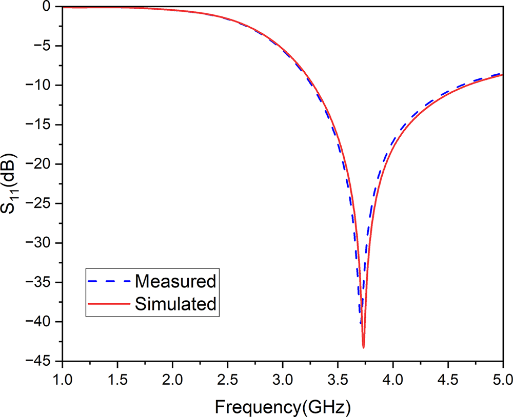
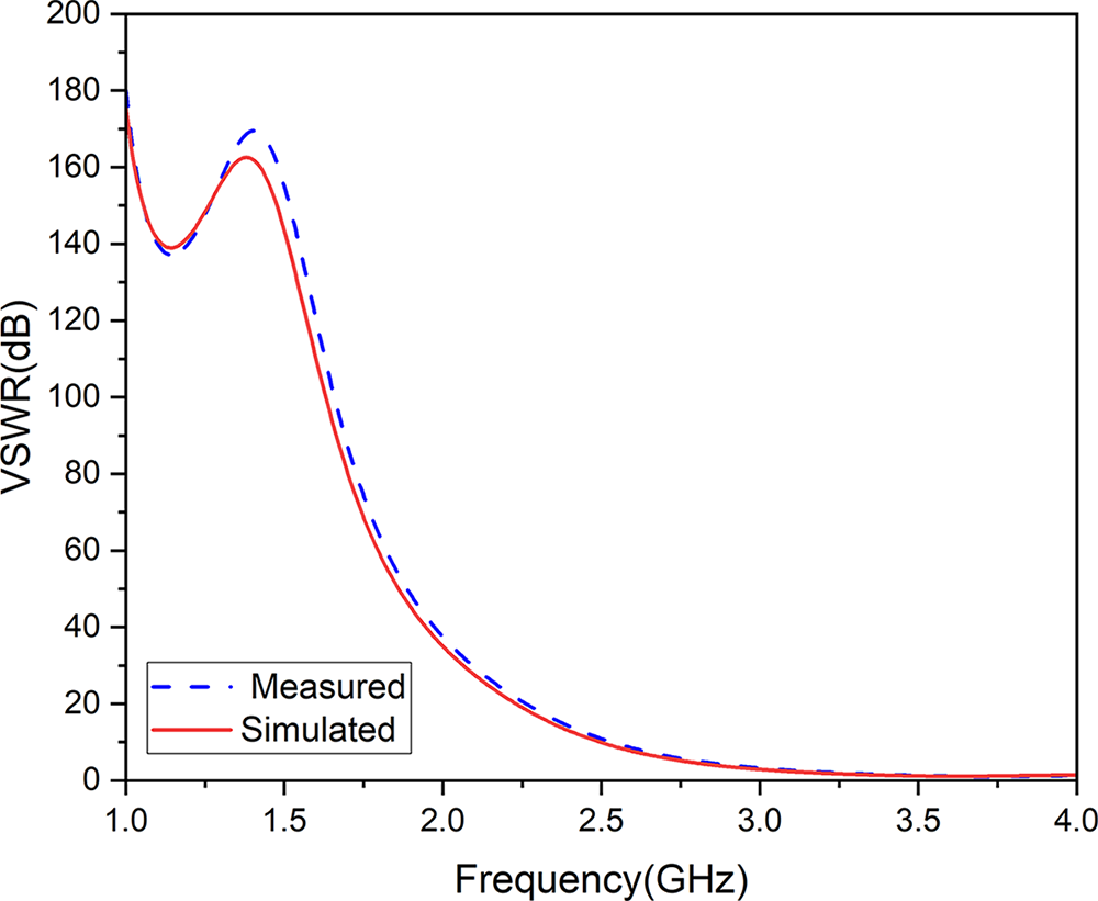
The result of the measured and simulated values for the proposed antenna design is compared now. Antenna design can be simulated using the software CST, and the Electromagnetic Anechoic Chamber can be used to measure the results of the proposed design. The measured and simulated antennas have bandwidth coverage at 1.36 GHz (3.26–4.62 GHz) at −10 dB. H-plane and E-plane of the far field are shown in Figure 4. The range of frequency for the omnidirectional antenna is simulated to have a gain of around 2.426 dBi at 3.7 GHz. The measured gain in dBi at a frequency range of −35.25 dBi at 2.5 GHz, −35.85 dBi at 3 GHz, and −39.65 dBi at 3.5 GHz is also observed. A VSWR <2 is observed with resonant frequencies, as shown in Figure 5. The presented antenna’s measured and simulated radiation patterns at various resonance frequencies are in good agreement with each other, as shown in Figure 6. So, the present antenna’s S11 return loss and resonant frequency are 3.7 and 3.64 GHz at −43.32 and −40.39 dB in simulated and measured results.
(a) E-plane radiation pattern for far-field and (b) H-plane radiation pattern for far-field.

VSWR Simulated result and VSWR measured result.

S11 Simulated result and S11 measured result.

Due to its partial ground configuration, as well as the flexible nature of the PDMS substrate that it uses, the antenna demonstrates quasi-bidirectional radiation with a front-to-back ratio of approximately 1.95 dB, which will be sufficient for body-centric wireless communications. The antenna has a cross-polarization of about 14 dB in the H-plane at 3.7 GHz, which indicates good polarization purity for wearable applications. The proposed antenna has a radiation efficiency of approximately 89% at 3.7 GHz and therefore has minimal dielectric and conductor loss, due to the flexible PDMS substrate that is being used. Therefore, the antenna has high efficiency and thus minimal dielectric and conductor loss, using the flexible PDMS substrate, and thus can be effectively utilized in wearable biomedical applications.
Compared to the measured and simulated results of the presented antenna, there is a good agreement between the two cases, as shown in Table 2.
Comparative analysis of measured and simulated results

The 3.7-GHz surface current distribution displays a high degree of current concentration in both the feed region and the edge regions of the radiating element. No surface current is present in the center of the radiating patch due to its lack of a metalized structure. The primary resonant path is therefore formed by the surface current flowing along the outer edge of the radiating patch, which dictates the effective electrical length of the antenna. Since there are no metallic structures within the central region of the radiating patch, no surface currents exist in this area.
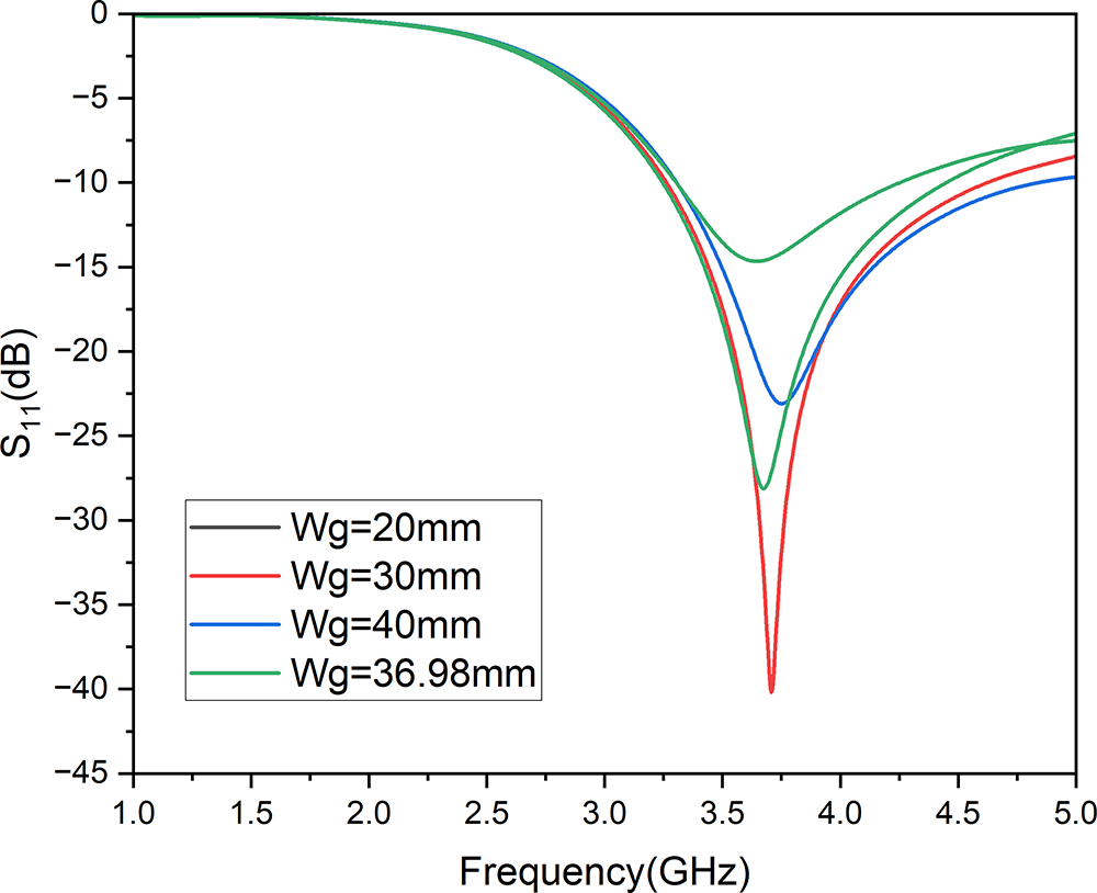
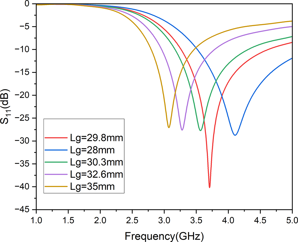
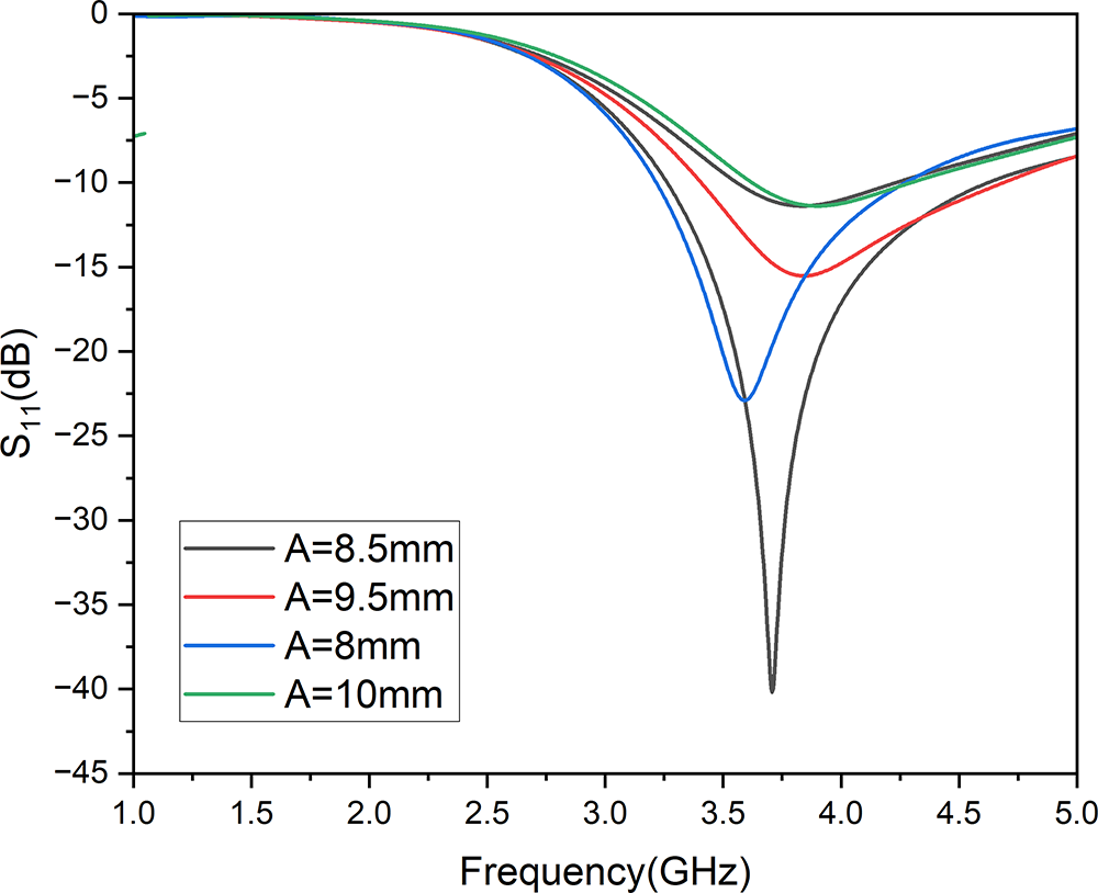
The proposed antenna is simulated for parametric sweep analysis in width W g from 20 to 40 mm, length L g from 27 to 35 mm, and radius A from 7 to 12 mm, where the analysis shows W g at 36.98 mm, L g at 29.8 mm, and A at 8.5 mm is the peak return loss, and the resonant frequency is 3.7 GHz at −43.32 dB in simulation, which is shown in Figures 7–9.
Simulated parametric sweep analysis in Width Wg from 20 mm to 40mm.

Simulated parametric sweep analysis in length Lg from 27 to 35 mm.

Simulated parametric sweep analysis in Radius A from 7 mm to 12 mm.

The variation of W g is seen to modify the return current path between the patch and the partial ground plane as well as the electromagnetic coupling between the patch and ground. Therefore, an increase in W g causes slight variations in both the impedance matching conditions of the antenna and the effective electrical length. Therefore, the resonant frequency of the antenna.
Thus, a partial ground current as a result of the return current generated by the partial ground is also part of the overall resonant current loop. Therefore, when L g is changed, this will affect the distribution of the return current between the return current path to the patch edge and the capacitive coupling of the return current to its opposite edge. The change in return current distribution will cause the input impedance characteristics to be altered, resulting in the resonance tuning that is being observed in the parametric analysis.
From Figure 10 (Surface Current Distribution at 3.7 GHz), we can see that the majority of the current flows along the perimeter of the circular patch. Therefore, by changing the diameter, we are effectively altering the length of the electric current flow path on the surface. In addition, as the radius increases, it also increases the electrical length of the boundary, which results in a downward movement of the resonant frequency. However, if we decrease the radius, we shorten the length of the current flow path, and this will result in an upward movement of the resonant frequency. Therefore, the trend exhibited in the parameter sweep is consistent with the observed trends in the surface current distribution.
Panels (a)–(c) show the surface current distribution at 3.2, 3.7, and 4.6 GHz.

Figure 10 Long description
Three surface-current distribution vector-field plots labeled (a), (b) and (c). Each plot shows a loop-shaped conductor outline above a rectangular base region, with many small arrow glyphs overlaid. Each plot includes a vertical color scale labeled A slash m with tick labels 0, 10, 20, 30, 40, 50, 60, 70 and 80. No x-axis label, y-axis label, spatial units, or coordinate ticks are visible. (a) The loop outline is tall and narrow. Arrow glyphs are densest at the junction where the loop meets the rectangular base region. A short horizontal red line segment is drawn near the bottom edge of the plotted area. (b) The loop outline is tall with a slightly wider upper section than (a). Arrow glyphs are densest at the loop-to-base junction. A short horizontal red line segment is drawn near the bottom edge of the plotted area. (c) The loop outline is wider and more rounded than (a) and (b). Arrow glyphs are densest at the loop-to-base junction. A short horizontal red line segment is drawn near the bottom edge of the plotted area. Across (a), (b) and (c), the shared scale indicates values span 0 to 80 A slash m and the highest-density arrow region is located at the loop-to-base junction in all three cases.
The performance of the presented flexible antenna is analyzed by comparison with the previous works, as shown in Table 3. The substrate of the presented antenna design is thin; hence, the vertical height of the antenna is reduced, so it is lightweight, which makes it suitable for the human body comfortably in real time. On the other hand, the proposed microstrip antenna provides broadband techniques of directional characteristics throughout the entire upper S-band and lower C-band region. The proposed antenna design is suitable for communication both on and off the body, which offers directional and omnidirectional radiation. The efficiency and gain of the presented antenna are more acceptable for practical applications.
Comparison of the proposed antenna with previous work

Table 3 Long description
Comparison of wearable and body-worn antennas by substrate, conductive material, physical size, operating frequency, gain, bandwidth, and intended application. Most designs use copper conductors; substrates include cotton, wool felt, felt with Teflon, jeans fabric, and PDMS. The proposed antenna uses PDMS with copper, measures 39.98 by 26.8 mm, operates at 3.7 GHz, has 2.42 dBi gain, and 1.36 GHz bandwidth for body-worn applications. Among PDMS designs, operating frequencies range from 2.92 to 5 GHz, with gains from 2.41 to 6.2 dBi and bandwidths from 820 MHz to 7.5 GHz. The highest gain listed is 6.54 dBi for a cotton and copper design at 2.40 GHz, while the lowest gain is 0.15 dBi for a jeans fabric and copper design at 2.45 GHz. Bandwidth reporting is inconsistent, with two entries showing no bandwidth value, so direct bandwidth comparisons across all rows are limited.
Bending analysis
To provide a deeper understanding of how the bending affects the operation of the antenna, the proposed antenna was mounted on two cylindrical surfaces having diameters of 2.5 cm (as shown in Figure 11(a)). As a result of the bending, there was a slightly greater difference in the resonant frequency and corresponding S11 value. However, despite this slight difference, the antenna continued to perform satisfactorily. Based upon the results from the previous study regarding the flexible characteristics of the PDMS substrate and the results of this experimental study, it has been concluded that, due to the bend-induced differences being relatively minimal when compared to those of the unbent condition, the proposed antenna continues to function effectively in a bent state.
(a) Front view of the proposed bending antenna and (b) S11 values under different bending conditions.

SAR analysis
In order to assess how the antenna will affect the human body, Specific Absorption Rate (SAR) analysis has been carried out with a simulation model. The SAR simulation model, as depicted in Figure 12 (a), is constructed as three layers. The uppermost layer represents the skin layer; the intermediate layer represents the fat layer; and the lowest layer represents the muscle layer. The properties of the human tissues have been taken from papers [Reference Sharma, Gupta and Dankov22, Reference Sharma and Gupta31]. The average SAR values resulting from the application of the simulation model using CST at 3.7 GHz with an input power of 100 mW are 1.9 W/kg, respectively, which is below the FCC safety limit of 1.6 W/kg. According to the European Standard, SAR should be less than 2 W/kg for a 10 g mass of average human tissue. The SAR values calculated for the proposed antenna at all of the resonant frequencies are below this limit.
(a) Simulation model and (b) a typical 3D customized phantom model.

Conclusion
A flexible electronic materials RF sensor for WLAN and WBAN applications is developed using a PDMS substrate and is presented in this article instead of rigid substrates. The proposed antenna has a 3.7 GHz resonant frequency with an overall size of 36.98 × 29.8 × 1 mm. Both the measured and simulated impedance bandwidths are <−10 dB with a range of 3.26–4.62 GHz, which is the desired range for wideband. Through a partial ground plane, feed structure dimensions and radiating element were changed to improve the proposed antenna performance. Throughout the whole wideband spectrum, good impedance matching was observed. Both measured and simulation results show good agreement with each other. The presented antenna is compared with recent research. The bending and analysis of SAR in this research study examines the effect of the antenna on human body tissue. It showcases that the proposed design of flexible antenna is appropriate for WBAN applications due to its compact size, simple geometrical configuration, economical fabrication process, flexibility, transparent and consistent performance under a wide range of operating conditions. When a PDMS-based antenna structure has been employed over a wideband range of frequencies in a wearable application, the prototype will be unique, novel, and effective in its characteristics. Hence, we have provided a simple, low-profile, novel, highly adaptable wearable RFID antenna/sensor for WBAN and 5G/6G applications.
Competing interests
The author(s) declare none.

V. Nisha Priyadharsini is currently pursuing the Ph.D. degree at Anna University, Chennai, India. Her research interests include wideband antennas, ultra-wideband (UWB) antennas, microwave engineering, and wireless communication systems. She is actively involved in research on the design and development of advanced antenna technologies for modern communication applications and emerging wireless networks.

Dr. K. Indhumathi is a distinguished technopreneur, academician, researcher, and innovator with expertise in Microwave Engineering. She is currently working as a Professor in the Department of Electronics and Communication Engineering at Rajalakshmi Institute of Technology, Chennai, India. She has contributed extensively in the areas of antenna design, phase shifters, RFID sensors, and biomedical applications of microwave systems. Alongside her academic role, she is actively engaged in promoting innovation and entrepreneurship among students and startups.

Dr. I. Balakrishna is a Joint Director/Scientist at the Research Centre, Chennai, under the Ministry of Electronics and Information Technology (MeitY), Government of India, with over 15 years of expertise in RF, microwave, and mmWave technologies. He specializes in advanced antenna design and RF systems, contributing to national defense projects and India’s indigenous 5G initiatives, including MIMO and massive MIMO. A published IEEE author and patent holder, he bridges academia and R&D, driving innovation in next-generation wireless and emerging RF technologies.