I. INTRODUCTION
Metal nanoclusters are the subject of numerous studies for applications in several fields, and the attention dedicated to this topic is witnessed by the increasing number of related contributions within the material science community. These nanoclusters exhibit striking optical propertiesReference Mazzoldi, Arnold, Battaglin, Gonella and Haglund1–Reference Karvianto and Chow3 and superparamagnetism with enhanced coercivity and a shift of their hysteresis loop.Reference de Julián Fernández, Sangregorio, Mattei, De, Saber, Lo Russo, Battaglin, Catalano, Cattaruzza, Gonella, Gatteschi and Mazzoldi4, Reference de Julián Fernández, Mattei, Maurizio, Cattaruzza, Padovani, Battaglin, Gonella, D’Acapito and Mazzoldi5
Tin (Sn) has been used since early 1960s as a solid-state gas sensor, and it became the main material commercially available in sensors for detecting fuel gas, carbon monoxide, general purpose combustible gases, ammonia, water vapor, etc. A considerable enhancement in the sensitivity was reported for Sn alloyed with noble metals.Reference Aroutiounian6, Reference Bonzi, Depero, Parmigiani, Perego, Sberveglieri and Quattroni7 Furthermore, alloying Sn thin films with copper (Cu) nanoclusters was found to enhance their sensing characteristics for gases such as H2S considerably.Reference Lee, Moon, Shim, Kim, Lee, Lee and Lee8–Reference Chowdhuri, Gupta and Sreenivas14 This makes such material particularly useful in industries where, e.g., leak detection and process control are significant issues. Therefore, in addition to the large surface area of Sn nanoclusters, alloying them with Cu is expected to further improve their sensing properties. However, to use those nanoclusters for applications, precise control of their size, yield, alloying concentration, and of size distribution is needed.
The present investigation focuses on the synthesis of pure Cu, pure Sn, and composite Cu–Sn nanoclusters using the magnetron sputtering technique inside an ultra-high vacuum (UHV) compatible system. This method of preparing composite Cu–Sn nanoclusters has many advantages: (i) nanoclusters are produced with a narrow size distribution; (ii) the average nanocluster size can be tuned by controlling the source conditions; (iii) no passivation layer is formed on the prepared nanoclusters, which provides direct access to their surface properties; (iv) a large portion of the produced nanoclusters are ionized, which allows size selection; (v) nanoclusters are self-assembled directly on a substrate without additional experimental stages; and (vi) the composition of nanoclusters can be controlled easily by varying the percentage of the metals within the sputtering target.
In this work, we investigate the composition of the produced nanoclusters and how to control their size and number by changing the source parameters. To the best of our knowledge, this is the first work that investigates the production parameters of composite Cu–Sn nanoclusters using the dc magnetron sputtering gas-condensation technique.
II. EXPERIMENTAL
Cu–Sn nanoclusters were synthesized using a magnetron sputtering plasma aggregation source inside the UHV compatible system.Reference Ayesh, Qamhieh, Ghamlouche, Thaker and El-Shaer15, Reference Ayesh, Thaker, Qamhieh and Ghamlouche16 The system consisted of two chambers: the source and main chambers, which were evacuated to a base pressure of ∼10−8 mbar. The dc magnetron-type discharge was utilized to generate nanoclusters from a target using a discharge power (P) of 15 W unless it is stated otherwise. For pure nanoclusters, Sn and Cu targets with purity of 99.995% were used. Composite nanoclusters were produced from Sn targets that were partially covered by Cu sheets (see inset of Fig. 2).Reference Ayesh, Qamhieh, Mahmoud and Alawadhi17 The percentages of Cu within the target that were used in this work were 33.3 and 66.6%, respectively. Argon (Ar) gas was used to generate the plasma, to sputter the material, and aggregate Cu–Sn nanoclusters from the target. A MKS Instruments mass flow controller (Andover, MA) was used to control the Ar flow rate (f) in the range of 10–100 sccm (sccm stands for standard cubic centimeter per minute). The magnetron gun was mounted on a motorized linear translator, enabling the aggregation length (L) to be varied by up to 100 mm (see Fig. 1 in Ref. Reference Ayesh, Thaker, Qamhieh and Ghamlouche16). The aggregation length is the distance from the surface of the sputtering target to the source exit nozzle. Ar gas inside the source chamber created a pressure difference between the source and the main chambers that forced the nanoclusters to travel through the quadrupole mass filter (QMF) and then to the main chamber. Ar gas was pumped away from the source and main chambers using two turbo pumps (for details, see Refs. Reference Ayesh, Qamhieh, Ghamlouche, Thaker and El-Shaer15 and Reference Ayesh, Thaker, Qamhieh and Ghamlouche16). The QMF was used to measure the nanocluster size distribution before its deposition inside the main chamber, with a maximum resolution U/V = 0.168 [a QMF is operated by connecting one pair of rods to a potential (U + Vcosωt) and the other to −(U + Vcosωt), where U is a dc voltage and Vcosωt is an ac voltage].Reference Dawson18 Assuming spherical nanoclusters, the size of a nanocluster refers to its diameter. A grid located at the exit of the mass filter—Faraday cup—was used to measure the electric current signal for ionized nanoclusters of each selected size, and the current was measured by a picoammeter. The area under a size distribution curve refers to the number of nanoclusters generated inside the source and detected using the Faraday cup. Thus, the area under a size distribution curve is defined in this context as the nanocluster yield. The size distribution measured by the QMF was also confirmed using a Philips CM10 transmission electron microscope (TEM; Hillsboro, OR). The nanocluster composition was measured using x-ray fluorescence (XRF) at four different locations for each sample to check the uniformity of their composition.
III. RESULTS AND DISCUSSION
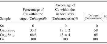
Nanoclusters produced in this study were generated using four targets: Sn, Cu, Cu1/3Sn2/3, and Cu2/3Sn1/3. Table I shows the percentage of Cu in the targets and in the produced nanoclusters (using f = 80 sccm, L = 80 mm, and P = 15 W). The Cu content within the nanoclusters is less than the nominal value in the target. The percentages of Cu in the produced nanoclusters are 58 and 65% of the nominal values in the targets Cu1/3Sn2/3 and Cu2/3Sn1/3, respectively [i.e., (Cu/nanocluster)/(Cu/target) = 58 and 68% for nanoclusters produced using Cu1/3Sn2/3 and Cu2/3Sn1/3 targets, respectively]. A more precise composition measurement of the individual nanoclusters can be performed using a high-resolution TEM.
The percentages of Cu–Sn in the targets and the produced nanoclusters.

The lower Cu content in the nanoclusters compared to that in the targets is explained in terms of nanocluster yield. The yields of different size distributions were measured as a function of the sputtering discharge power and illustrated in Fig. 1. The figure shows that, within the studied discharge power range, Sn has a higher nanocluster yield. Nanoclusters of a material can be produced within an optimum power range: low power leads to low self-bias on the target, while high power produces unstable plasma.Reference Ohring19, Reference Pratontep, Carroll, Xirouchaki, Streun and Palmer20 Therefore, the lower Cu contents within nanoclusters than that in the targets can be a result of the lower nanocluster yield of Cu compared to Sn. This can be rationalized in terms of the fact that Cu has a smaller atomic mass than Sn. The smaller the mass, the higher the drift velocity (shorter nucleation and growth time), and thus, the lower the Cu content. Owing to the higher nanocluster yield of Sn compared to Cu, and less amount of Sn within the target for Cu2/3Sn1/3 nanoclusters, the ratio (Cu/nanocluster)/(Cu/target) is less for nanoclusters produced using Cu2/3Sn1/3 target than that produced using Cu1/3Sn2/3 target. It should be noted that in the following discussion, composite nanoclusters will be named following their source target, i.e., Cu1/3Sn2/3 and Cu2/3Sn1/3, although they exhibit different composition ratios.
The dependence of Cu and Sn nanoclusters’ yield on the sputtering discharge power.

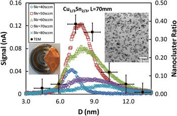
Figure 2 shows the size distributions of Cu1/3Sn2/3 nanoclusters produced for L = 70 mm and different Ar flow rates. The produced nanoclusters exhibit narrow size distributions with full width at half maximum between 1.55 and 5.3 nm. Two main features can be observed in the figure: (i) a shift of the maximum (the average nanocluster size, D) toward higher sizes with increasing f and (ii) variation of the area under each size distribution curve (nanocluster yield), where the area increases with increasing f up to 50 sccm and then it decreases. The investigation of the dependence of nanocluster size and yield on the source parameters (f and L) provides an understanding of the formation mechanisms of the produced nanoclusters. Hence, a size distribution curve was produced for each value of f and L.
Size distributions of nanoclusters produced using Cu1/3Sn2/3 target at different Ar flow rates and L = 70 mm. The filled circles are the size distribution as measured from the TEM image. The insets are: image of the Cu1/3Sn2/3 target (left)Reference Ayesh, Qamhieh, Mahmoud and Alawadhi17 and a TEM image of Cu1/3Sn2/3 nanoclusters produced using the above conditions with f = 50 sccm (right).

The inset of Fig. 2 shows an example of a TEM image for Cu1/3Sn2/3 nanoclusters produced using f = 50 sccm and L = 70 mm. The size distribution was measured from the TEM image and it is presented in Fig. 2 as well. The size distributions measured using the QMF and the TEM image are in good agreement.
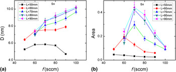
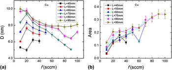
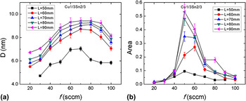
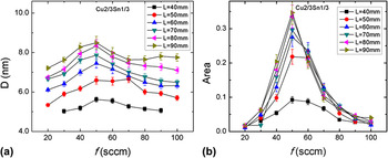
Figures 3(a), 4(a), 5(a), and 6(a) show the dependence of average nanocluster size on f at different aggregation lengths for Sn, Cu, Cu1/3Sn2/3, and Cu2/3Sn1/3, respectively. Each error bar in the figures is the standard deviation of the size distribution curve. The small standard deviation indicates that monodispersed nanoclusters are formed. These figures show that increasing the aggregation length generally increases the average size of nanoclusters. Figure 3(a) reveals that the average size of the Sn nanoclusters increases with increasing f for L between 60 and 90 mm. Small variations in the size with increasing f are observed for L = 50 mm (the variation is between 4.7 and 5.8 nm). For Cu nanoclusters [Fig. 4(a)], the size decreases with increasing f for large aggregation lengths (L = 80 and 90 mm). On the other hand, for lower aggregation lengths (L = 50–70 mm), D increases with increasing f up to 20 sccm, and then, it decreases. For L = 40 mm, the average size increases with increasing f. For composite Cu1/3Sn2/3 nanoclusters, shown in Fig. 5(a), D increases with f and shows a maximum at about 70 sccm. A similar trend is observed for the Cu2/3Sn1/3 nanoclusters [in Fig. 6(a)]; however, the D(f) dependence is weaker, and the maximum sizes were achieved around f = 50 sccm.
The dependence of the Sn nanocluster (a) average size and (b) yield on Ar flow rate for different aggregation lengths.

The dependence of Cu nanocluster (a) average size and (b) yield on f for different aggregation lengths.

The dependence of Cu1/3Sn2/3 nanocluster (a) average size and (b) yield on Ar flow rate for different aggregation lengths.

The dependence of Cu2/3Sn1/3 nanocluster (a) average size and (b) yield on f for different aggregation lengths.

The direct increase of D with L, illustrated in Figs. 3(a), 4(a), 5(a), and 6(a), can be understood in terms of the nanocluster nucleation and growth time. Increasing the aggregation length causes the nanoclusters to remain longer within the aggregation region, which in turn promotes their growth.
As the inert gas flow rate increases inside the source chamber, the thermalization and nanocluster formation processes are disturbed in the gas stream. Computer simulation for each nanocluster source design would be useful for a better understanding of the details of the gas stream inside the nanocluster source, thus, the thermalization process.Reference Knuth21 Herein, the type of collision involved in nanocluster production can be used to explain the variation of D as a function of f. Nanocluster nucleation and growth occur using one or both of the following mechanisms: (i) three-body collision in which two sputtered atoms lose their excess kinetic energy by colliding with an Ar atom and (ii) two-body collision in which nanocluster growth occurs via nanocluster–atom (atomic condensation) and nanocluster–nanocluster collisions.Reference Banerjee, Krishna and Das22, Reference Haberland23 Nanocluster seeds are initiated through three-body collision due to cooling of the sputtered atoms by Ar atoms. The probability of the three-body collision is determined by the density of atomic vapor and the nucleation and growth times. Thus, for the three-body collision mechanism, nanocluster size is expected to decrease as f increases because of the high drift velocity of the material within the growth region (i.e., the nucleation and growth time decreases).Reference Banerjee, Krishna and Das22 Herein, the number of metal atoms (or small nanoclusters) that can combine with a nanocluster decreases as f increases, thus, nanocluster growth is reduced.Reference Yamamuro, Sumiyama, Sakurai and Suzuki24 The nanoclusters grow further by the two-body collision mechanism.Reference Hihara and Sumiyama25 When the two-body collision mechanism is dominant, larger nanoclusters are produced.Reference Ayesh, Qamhieh, Ghamlouche, Thaker and El-Shaer15, Reference Hihara and Sumiyama25 As f increases, the mean free path decreases and this in turn increases the probability of the two-body collision, which allows further nanocluster–atom and nanocluster–nanocluster collisions.Reference Yamamuro, Sumiyama, Sakurai and Suzuki24 Therefore, the increase of D with f for Sn [Fig. 3(a)] indicates the dominance of the two-body collision mechanism, while the decrease in D with f for Cu [Fig. 4(a)] shows the dominance of the three-body collision mechanism. It should be noted that Cu nanocluster formation is dominated by the two-body collision mechanism for f < 20 sccm and L < 80 mm, as evidenced by the increase of D with f in Fig. 4(a).
For the composite nanoclusters, the observed maxima in nanocluster size with f indicate that both collision mechanisms contribute to the formation of nanoclusters. Since the three-body collision mechanism is dominant for Cu and the two-body collision mechanism is dominant for Sn nanoclusters, the difference in the rate of increase in D with f, shown in Figs. 5(a) and 6(a), can be attributed to the contribution percentage of the two collision mechanisms for Cu1/3Sn2/3 and Cu2/3Sn1/3 nanoclusters. Thus, at low f, the larger increase in the size with f for Cu1/3Sn2/3 (compared to that for Cu2/3Sn1/3) is a result of the larger percentage of Sn and, hence, the larger contribution of the two-body collision mechanism. At high flow rates, a smaller decrease in D is observed in Figs. 5(a) and 6(a), which can be related to the lower rate of decrease in Cu nanocluster size with f. It should be mentioned here that the smaller slopes of increase and decrease in Figs. 5(a) and 6(a), compared to those in Figs. 3(a) and 4(a), are an indication of the contribution of both nucleation mechanisms (two-body and three-body collisions) in the formation of nanoclusters at all Ar flow rates, albeit at different rates.
The dependence of the area under the size distribution curves on f and L for Sn, Cu, Cu1/3Sn2/3, and Cu2/3Sn1/3 is shown in Figs. 3(b), 4(b), 5(b), and 6(b). The figures show that increasing the aggregation length increases the area under each size distribution curve, indicating an increase in the nanocluster yield. For Sn nanoclusters [Fig. 3(b)], small areas can be observed at low f, which increases to a maximum value and then decreases with f. However, in Fig. 4(b), the Cu nanocluster yield keeps increasing with f. Figures 5(b) and 6(b) for Cu1/3Sn2/3 and Cu2/3Sn1/3 show that the yield increases with f, exhibits a maximum around 50 sccm, and then decreases.
The increase in the nanocluster yield with L is due to the long nucleation and growth time, which supports nanocluster growth and yield. The decrease in the nanocluster yield with f, observed in Fig. 3(b), is a result of consuming the nanoclusters to produce larger nanoclusters. This argument is consistent with the result of Fig. 3(a), where the increase in D with f is mainly due to nanocluster–nanocluster (two-body) collision mechanism. The small number of produced nanoclusters at low f, observed in Fig. 3(b), appears for all curves with L > 50 mm and could be the result of low nanocluster yield of Sn at the lowest possible f. Furthermore, the increase in nanocluster yield with f for Cu in Fig. 4(b) is a result of the dominance of the three-body collision mechanism. Herein, the decrease in D with f observed in Fig. 4(a) indicates that the sputtered material is used up to produce additional small nanoclusters, in other words, more nanocluster yield. The dependence of the yield on f for composite nanoclusters [Figs. 5(b) and 6(b)] is a result of the combined nanocluster nucleation and growth mechanisms (two- and three-body). Nanocluster growth via the two-body collision mechanism involves either nanocluster–nanocluster collisions or/and nanocluster–atom collisions. The probability of these collisions governs the number of produced nanoclusters.Reference Haberland23 The nanocluster yield is expected to increase with f if the nanocluster–atom collision is dominant and more condensation occurs. Nevertheless, the nanocluster yield is likely to decrease with f if the nanocluster–nanocluster collision is dominant because nanoclusters are expended to produce larger ones.Reference Hihara and Sumiyama25 Therefore, the maxima at f = 50 sccm in Figs. 5(b) and 6(b) indicate that the nucleation and growth are dominated by three-body and two-body (nanocluster–atom) collision mechanisms. The small number of nanoclusters at low f indicates that their production is determined mainly by the two-body (nanocluster–nanocluster) collision mechanism as evident in Figs. 3 and 4. Thus, nanoclusters are consumed to generate larger ones. Nevertheless, the low yield at high f might be assigned to a larger contribution of the nanocluster–nanocluster collision compared to the three-body collision mechanism, which could be attributed to the larger mass of Sn atoms (smaller mean-free-path).
IV. CONCLUSIONS
Composite copper–tin (CuxSn1−x) nanoclusters were fabricated using the magnetron sputtering technique inside a UHV compatible system. Nanoclusters with different Cu to Sn ratios were produced by changing the ratio of Cu to Sn within the target. The dependence of the yield and size of nanoclusters on the source conditions reveal two nucleation and growth mechanisms: two-body and three-body collisions. The detailed study showed that the former dominates in Sn nanocluster nucleation and growth processes, while the latter dominates in Cu nanocluster nucleation and growth processes. However, for composite nanoclusters, the two-body collision mechanism was dominant for low f, while three-body collision mechanism was dominant for high f. This work demonstrates the ability of producing composite CuxSn1−x nanoclusters and controlling their size and yield by tuning the source operating conditions.
ACKNOWLEDGMENTS
This work was supported by United Arab Emirates University under the Grant No. FOS/IRG-23/11. The authors would like to thank Mr. S. Tariq at FMHS, United Arab Emirates University for TEM images. Also they would like to thank the National X-ray Fluorescence Lab at the University of Sharjah for XRF analysis.