


Introduction
Dynamic random-access memory (DRAM) has served as the main memory in modern computers since it was introduced by Intel Corporation in 1972. DRAM is widely used in modern computers owing to characteristics such high-speed operation, large integration density, and excellent reliability.
A DRAM cell has a simple structure comprising one capacitor (1C) connected by one transistor (1T) (1T-1C) to the bit line (the line through which information is written to/read from the memory cell) (Figure 1a). The access transistor is connected to the word line and acts as a switch. The capacitor stores each bit of data as a negative or positive electrical charge. The memory state is read by sensing the stored charge on the capacitor via the bit line, which is set to V cc/2, (V cc: operating voltage of the chip) with the transistor closed. When the access transistor is on, the stored charge carriers flow into the bit line, which changes its potential. This voltage change is detected and amplified by the sense amplifier connected to the bit line.
(a) Structure of a 1-transistor-1-capacitor (1T-1C) dynamic random-access memory (DRAM) cell. (b) Timing of DRAM technology nodes reported in the International Technology Roadmap for Semiconductors (ITRS).Reference Hwang1

During the past several decades, exponential growth in the number of memory cells per chip has occurred. Perpetual memory cell scaling has been the major strategy for realizing rapid increases in memory density.Reference Hwang1 DRAM is amenable to scaling because of its simple structure, and scaling of DRAM down to a ∼100-nm technology node (specific manufacturing process and its design rule) is easily achieved with traditional materials such as Si-based dielectrics (SiO2 and SiNx) and electrodes (poly-Si). This excellent scalability of DRAM has led to its long-lasting success. Today, much effort is devoted to accelerating the scaling of DRAM cells further to the ∼10-nm technology node2 (Figure 1b).
DRAM is a charge-based RAM that requires a certain cell capacitance value (∼10 fF/cell) to secure the minimum voltage difference detectable by the sense amplifier, regardless of cell size. The ever-shrinking dimension of the capacitor in DRAM cells will eventually result in failure to meet this cell capacitance requirement. Hence, advancing capacitor technology is essential for continued scaling of DRAM. The scaling of the DRAM cells also raises problems in the access transistor. Without major innovations in structure, materials, and processing, scaling of DRAM will end soon.
Transistor technology in DRAM
Unlike the transistor in performance-oriented logic devices, the access transistor in DRAM requires a high ON/OFF current ratio (∼108) to prevent substantial loss of the charges stored in the capacitor and to write the data within a short time (less than a few tens of a nanosecond). As the DRAM cell shrinks, obtaining sufficient data retention time becomes more challenging. The increase in the channel doping concentration with scaling of the feature size results in increased electrical field and junction leakage current. A simple and effective way to overcome this detrimental short-channel effect is to increase the channel length. Three-dimensional (3D) structured transistors such as recess-channel-array transistors (RCATs) have been used to increase the effective channel length in this restricted dimension (Figure 2a).Reference Kim, Lee, Kim, Chung, Choi, Park, Lee, Kim, Hwang, Hwang, Hwang, Park, Kim, Kang, Cho, Jeong, Kim, Han, Kim, Nam, Park, Chung, Lee, Park, Kim, Park and Kim3 Further increase in the channel length has been achieved by using modified RCAT structures such as sphere-shaped RCATReference Kim, Oh, Woo, Lee, Kim, Kim, Ha, Kim, Kang, Park, Hwang, Kim, Park, Huh, Lee, Kim, Cho, Jung, Kim, Jin, Shin, Shim, Lee, Lee, Park, Jin, Park and Kim4 and U-shaped RCATReference Lee, Park, Park, Lee, Hong, Kim, Choi, Lee, Jin and Kim5 (Figure 2a). Below a technology node of ∼50 nm, saddle-fin transistors, which combine fin-shaped field-effect transistor with a RCAT, have been utilized to obtain superior current-driving capability and sufficient data retention time.Reference Park, Han and Lee6,Reference Yang, Wei, Chang, Wu, Chen and Lai7
(a) Channel structure evolution of the cell transistor in dynamic random-access memory.Reference Kim, Oh, Woo, Lee, Kim, Kim, Ha, Kim, Kang, Park, Hwang, Kim, Park, Huh, Lee, Kim, Cho, Jung, Kim, Jin, Shin, Shim, Lee, Lee, Park, Jin, Park and Kim4,Reference Lee, Park, Park, Lee, Hong, Kim, Choi, Lee, Jin and Kim5,Reference Yang, Wei, Chang, Wu, Chen and Lai7,Reference Schloesser, Jakubowski, Kluge, Graham, Slesazeck, Popp, Baars, Muemmler, Moll, Wilson, Buerke, Koehler, Radecker, Erben, Zimmermann, Vorrath, Fischer, Aichmayr, Agaiby, Pamler, Schster, Bergner and Mueller9 Transmission electron microscope (TEM) images of (i) RCAT, (ii) S-RCAT, and (iii) U-RCAT. (iv) (Middle) Schematic of a saddle-fin transistor with TEM cross-section images of the (left) x- and (right) y-axes of the transistor. (v) Cross-sectional image of a buried word line with a saddle-fin channel configuration. (b) (Upper) Layout of a 4 F2 cell and (lower) schematic of a 4 F2 cell with vertical pillar transistor.Reference Chung, Kim, Kim, Kim, Kim, Song, Kim, Oh, Hwang, Hong, Jin and Chung10 Note: F, minimum feature size; RCAT, recess-channel-array transistor; S-RCAT, sphere-shaped RCAT; U-RCAT, U-shaped RCAT; D, drain; S, source; BL, bit line; CC, cell capacitor; WL, word line; VPT, vertical pillar transistor.
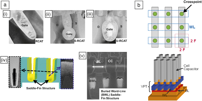
An 8 F2 (where F is the minimum feature size) cell design architecture with a folded bit-line structureReference Hwang, Kim, Lee and Hwang8 has been traditionally used in DRAM because of reliable operations for the cell architecture. However, the demand for further scaling of the DRAM cell (< ∼80-nm technology node) has resulted in conversion from 8 F2 to 6 F2 cell design architecture with an open bit line, because the 6 F2 design provides a 25% improvement in DRAM cell area. However, the open bit-line architecture is vulnerable to array noise because of the high bit-line capacitance. A buried word line (Figure 2a), which is placed below the Si surface, is currently used to relieve this noise vulnerability.Reference Schloesser, Jakubowski, Kluge, Graham, Slesazeck, Popp, Baars, Muemmler, Moll, Wilson, Buerke, Koehler, Radecker, Erben, Zimmermann, Vorrath, Fischer, Aichmayr, Agaiby, Pamler, Schster, Bergner and Mueller9 A new 4 F2 cell architecture—the most compact cell structure (Figure 2b) with a vertical pillar transistor—has also been proposed to facilitate further DRAM cell scaling.Reference Chung, Kim, Kim, Kim, Kim, Song, Kim, Oh, Hwang, Hong, Jin and Chung10 The shift of cell architecture from 6 F2 to 4 F2 results in a 33% cell-area reduction. In the 4 F2 cell design, the transistor and capacitor lie at every crosspoint of the word lines and bit lines. The vertical pillar transistor is placed on the buried bit line and beneath the storage node (Figure 2b). This cell design is highly favorable to lower the bit-line capacitance, due to the distinct arrangement of the buried bit line, aside from the capacitor. However, transiting from 6 F2 to 4 F2 DRAM cell design is still challenging. For further scaling of DRAM cells, severe technological challenges such as the floating body effect of the channel in the vertical transistor (the channel in the vertical transistor is isolated from the Si substrate), structural vulnerability of the pillar channel, and high resistance of the bit line remain.
Capacitor technology in DRAM
For successful DRAM cell operation, the capacitor in the DRAM cell should meet two requirements—sufficient capacitance (∼10 fF/cell) and ultralow leakage current (J g < 10–7 A/cm2 at the operating voltage) irrespective of the cell size. The cell capacitance is expressed by:
 $$C = \varepsilon _0 k{A \over {t_{{\rm{phys}}} }},$$
where C, ε0, k, A, and t phys are the capacitance, vacuum permittivity, dielectric constant, effective capacitor area, and the physical thickness of the dielectric layer, respectively. Scaling of the DRAM cell has continuously reduced the area allocated to the capacitor in the cell, such that a 3D structured capacitor is used to obtain the necessary capacitance in the limited area, as shown in Figure 3a.Reference Kim, Lee, Han, Lee, Han and Hwang11 The aspect ratio of the capacitor has sharply increased and will reach ∼100 shortly because of the aggressive scaling of DRAM. However, further increase in the aspect ratio is impossible because of the structural vulnerability of the storage node. Thinning of the dielectric layer is also not an eventual solution to acquire large capacitance as the electric field applied to the dielectric increases with decreasing t phys, which leads to a significant rise in the J g.
(a) Summary of dynamic random-access memory (DRAM) capacitor technology evolution.Reference Kim, Lee, Han, Lee, Han and Hwang11 (b) Schematic of pillar-type capacitors. (c) J g at ±1 V as a function t phys and EOT (nm) values for SrTiO3 (denoted STO) (●),Reference Swerts, Popovici, Kaczer, Aoulaiche, Redolfi, Clima, Caillat, Wang, Afanas’ev, Jourdan, Olk, Hody, Elshocht and Jurczak17,Reference Popovici, Swerts, Redolfi, Kaczer, Aoulaiche, Radu, Clima, Everaert, Elshocht and Jurczak48 and nanolaminates: TiO2/ZrO2/TiO2 (denoted TZT) and TiO2/ZrO2/Al2O3/ZrO2/TiO2 (denoted (TZAZT) (◀),Reference Padmanabhan, Mohan, Morozumi, Kaushal and Bhat49 ZrO2/HfLaO/ZrO2 (denoted Z/HL/Z)(▼)Reference Shin, Min, Lee, Lim, Oh, Lee, Hong and Cho50 and ZrO2/SrO(or Al2O3)/ZrO2 (ZSrZ or ZAZ) (◆).Reference Knebel, Pešić, Cho, Chang, Lim, Kolomiiets, Afanas’ev, Muehle, Schroeder and Mikolajick20 In the case of ATO(■)Reference Jeon, Yoo, Kim, Lee, An, Chung, Cho, Kim and Hwang41 and Si:HZO(▲)Reference Ahn and Kwon51 (Si doped Zr60Hf40 oxide), J g is reported at 0.8 V. ZrO2-based dielectrics remain the most promising path toward the envisaged EOT-J g values at ≤5 nm t phys. Note: SIS, silicon–insulator–silicon; MIS, metal–insulator–silicon; MIM, metal–insulator–metal; ATO, Al-doped TiO2; J g, leakage current; t phys, physical thickness of the dielectric layer; EOT, equivalent oxide thickness; F, minimum feature size.

Therefore, a higher-k material must be used as the dielectric in the DRAM capacitor. The t phys value can be increased to some extent owing to the high-k value, reducing the effective electric field at the operating voltage. The figure of merit used by DRAM capacitor technology is the electrical performance of the dielectric material as compared to SiO2, known as the equivalent oxide thickness (EOT). The EOT of the dielectric is given by:
 $$EOT = {{3.9 \times t_{{\rm{phys}}} } \over k},$$
where 3.9 is the dielectric constant of SiO2. In the last decade, extensive investigations have focused on identifying high-k dielectrics in conjunction with specific metal electrodes to reduce the EOT value.Reference Kim, Lee, Han, Lee, Han and Hwang11–Reference Knebel, Pešić, Cho, Chang, Lim, Kolomiiets, Afanas’ev, Muehle, Schroeder and Mikolajick20
DRAM capacitor technology is more seriously challenged than ever. Sub-20-nm DRAM technology nodes require a low EOT value of <0.5 nm, which is difficult to achieve. A significant challenge is the limit in t phys of the dielectric and electrode layers. For >40-nm technology nodes, the lateral size of the capacitor is incomparably larger than the t phys of the layers. This large technology node enables the use of cylindrical capacitors to maximize the effective capacitor area. For sub-20-nm technology nodes, however, the cylindrical structure is no longer valid and pillar capacitors are utilized because of their small feature size (F < 20–40 nm) (Figure 3a). The t phys of the dielectric is stringently limited below ∼5 nm, even in the pillar structure, because the sum of 2 × t phys, width of the bottom electrode, and the thickness of the top electrode should not exceed 2 × F (Figure 3b). A new high-k material for future DRAM capacitors should achieve both ultralow J g (10–7 A/cm2 at the operating voltage) and a low EOT of <0.5 nm at a low thickness of <5 nm.
Dielectrics in DRAM capacitors
The dielectric layer should be conformally formed over the 3D capacitor structure. A better step coverage is necessary at a lower t phys, because the electric field at a thinner layer can be significantly influenced by even a tiny difference in the t phys. Atomic layer deposition (ALD), known to achieve exceptional step coverage, is appropriate for the growth of the dielectric layer over the 3D capacitor. In addition, ALD can grow high-quality films at a relatively low temperature. Consequently, the ALD technique has been extensively used for studies on the dielectric in DRAM capacitors.
DRAM capacitor technology has relied on the ZrO2 dielectric for a decade as it enabled attainment of the 25-nm technology node. The trilayer structure of tetragonal (or cubic ZrO2 (k ≈ 40))/amorphous Al2O3 (k ≈ 9)/tetragonal (or cubic ZrO2), called ZAZ, in combination with TiN electrodes has replaced HfO2 for the capacitors required for the ≤45-nm technology node.Reference Kil, Song, Lee, Hong, Kim, Park, Yeom, Roh, Kwak, Sohn, Kim and Park21 Nevertheless, it is generally agreed that a J g of 10–7 A/cm2 at ±1 V cannot be maintained with the ZAZ nanolaminate stack for a sub-20-nm technology node with smaller surface areas that involves reducing t phys of the dielectric.2
RobertsonReference Robertson22 showed that the k of oxides tends to vary inversely with the bandgap, which limits the choice of high-k oxides to several candidates comprising TiO2 and SrTiO3. Their bandgap is rather small (3.2–3.3 eV); however, their k values are more than 100. Although the allowable cation nonstoichiometry range of bulk SrTiO3 is narrow and off-stoichiometric SrTiO3 thin films usually show decreased k value, its perovskite structure could be maintained in a reasonable range of Sr:Ti ratios around stoichiometric SrTiO3.Reference Menou, Popovici, Clima, Opsomer, Polspoel, Kaczer, Rampelberg, Tomida, Pawlak, Detavernier, Pierreux, Swerts, Maes, Manger, Badylevich, Afanasiev, Conard, Favia, Bender, Brijs, Vandervorst, Elshocht, Pourtois, Wouters, Biesemans and Kittl14,Reference Popovici, Van Elshocht, Menou, Swerts, Pierreux, Delabie, Brijs, Conard, Opsomer, Maes, Wouters and Kittl23 Significant efforts have been devoted to the development of SrTiO3Reference Menou, Popovici, Clima, Opsomer, Polspoel, Kaczer, Rampelberg, Tomida, Pawlak, Detavernier, Pierreux, Swerts, Maes, Manger, Badylevich, Afanasiev, Conard, Favia, Bender, Brijs, Vandervorst, Elshocht, Pourtois, Wouters, Biesemans and Kittl14,Reference Pawlak, Swerts, Popovici, Kaczer, Kim, Wang, Tomida, Govoreanu, Delmotte, Afanas’ev, Schaekers, Vandervorst and Kittl16,Reference Swerts, Popovici, Kaczer, Aoulaiche, Redolfi, Clima, Caillat, Wang, Afanas’ev, Jourdan, Olk, Hody, Elshocht and Jurczak17,Reference Popovici, Van Elshocht, Menou, Swerts, Pierreux, Delabie, Brijs, Conard, Opsomer, Maes, Wouters and Kittl23–Reference Lee, Jeon, An, Chung, Kim, Eom, George, Park, Han, Kim, Chung, Lee and Hwang33 and TiO2Reference Kim, Kim, Kim, Hwang and Jeong12,Reference Fröhlich, Aarik, Ťapajna, Rosová, Aidla, Dobročka and Hušková13,Reference Kim, Kim, Jeong, Jeon, Yoon and Hwang18,Reference Kim, Lee, Seo, Choi and Hwang34,Reference Kim, Hwang, Kwon, Kim, Cho, Jeong, Lee, Seo, Hwang, Min and Cho35 by ALD. High-k values of SrTiO3 while preserving low J g could be achieved by controlling the stoichiometry (Sr enrichment)Reference Pawlak, Swerts, Popovici, Kaczer, Kim, Wang, Tomida, Govoreanu, Delmotte, Afanas’ev, Schaekers, Vandervorst and Kittl16,Reference Swerts, Popovici, Kaczer, Aoulaiche, Redolfi, Clima, Caillat, Wang, Afanas’ev, Jourdan, Olk, Hody, Elshocht and Jurczak17 or the grain size.Reference Kwon, Lee, Han and Hwang27,Reference Popovici, Kaczer, Afanas’ev, Sereni, Larcher, Redolfi, Elshocht and Jurczak30
TiO2 crystallizes as anatase (k ≈ 40) or rutile (k ≈ 80) phases. Rutile, a high-temperature phase,Reference Kadoshima, Hiratani, Shimamoto, Torii, Miki, Kimura and Nabatame36 is incompatible with the thermal budget required in the DRAM fabrication process (<600°C). However, when grown on RuO2 conductive oxide, rutile TiO2 phase with similar lattice parameters crystallizes at deposition temperatures (i.e., 250°C) owing to the template effect displayed by the substrate,Reference Kim, Kim, Kim, Hwang and Jeong12,Reference Fröhlich, Aarik, Ťapajna, Rosová, Aidla, Dobročka and Hušková13,Reference Popovici, Swerts, Tomida, Radisic, Kim, Kaczer, Richard, Bender, Delabie, Moussa, Vrancken, Opsomer, Franquet, Pawlak, Schaekers, Altimime, Van Elshocht and Kittl37,Reference Kim, Hwang, Kim and Hwang38 thus reducing both the EOT and J g.Reference Kim, Kim, Kim, Hwang and Jeong12,Reference Popovici, Kim, Tomida, Swerts, Tielens, Moussa, Richard, Bender, Franquet, Conard, Altimime, Elshocht and Kittl15,Reference Kim, Lee, Seo, Choi and Hwang34 Nevertheless, the scalability of t phys is limited to 10–12 nm. Doping TiO2 with AlReference Kim, Lee, Han, Lee, Han and Hwang11,Reference Kim, Choi, Lee, Seo, Lee, Han, Ahn, Han and Hwang39–Reference Choi, Kim, Won, Kim and Hwang42 could further reduce J g, leading to further reduction in t phys to ∼7 nm.Reference Kim, Choi, Lee, Seo, Lee, Han, Ahn, Han and Hwang39,Reference Jeon, Yoo, Kim, Lee, An, Chung, Cho, Kim and Hwang41
A doping approach could also be considered for other dielectrics (e.g., HfO2 and ZrO2). Dopants with lower electronegativities and larger ionic radii than those corresponding to the host oxide led to higher-k and a reduction of J g for HfO2Reference Chen, Liu, Feng, Che and Zhao43–Reference Govindarajan, Böscke, Sivasubramani, Kirsch, Lee, Tseng, Jammy, Schröder, Ramanathan and Gnade45 and ZrO2.Reference Lamagna, Wiemer, Baldovino, Molle, Perego, Schamm-Chardon, Coulon and Fanciulli46,Reference Park, Oh, Mahata, Lee, Thompson, Lee, Maeng and Kim47 Higher symmetry phases are formed via doping (such as tetragonal or cubic) leading to larger k, while the lower J g was attributed to the shift of the charge states of the oxygen vacancies into the conduction bands.Reference Park, Oh, Mahata, Lee, Thompson, Lee, Maeng and Kim47
As previously described, continued downscaling of DRAM technology toward the sub-20-nm technology node will require a low t phys of ≤5 nm. At such a low thickness, other characteristics of the capacitors become important, including electrode and dielectric surface roughness, lattice mismatch, and chemical compatibility of electrode/dielectric. A summary of the lowest EOT – J g – t phys at ±1 V for ALD dielectrics is given in Figure 3c.Reference Swerts, Popovici, Kaczer, Aoulaiche, Redolfi, Clima, Caillat, Wang, Afanas’ev, Jourdan, Olk, Hody, Elshocht and Jurczak17,Reference Knebel, Pešić, Cho, Chang, Lim, Kolomiiets, Afanas’ev, Muehle, Schroeder and Mikolajick20,Reference Jeon, Yoo, Kim, Lee, An, Chung, Cho, Kim and Hwang41,Reference Popovici, Swerts, Redolfi, Kaczer, Aoulaiche, Radu, Clima, Everaert, Elshocht and Jurczak48–Reference Ahn and Kwon51 This shows that the nanolaminates’ approach combining a high bandgap with a high-k dielectric leads to the lowest J g when thinning the dielectric. However, for t phys ≤ 5 nm, the nanolaminate approach is less likely to be an option because of intermixing of the layers under the thermal budget applied to the capacitor.
Comprehensive ab initio calculations of the bandgap and k Reference Yim, Yong, Lee, Lee, Nahm, Yoo, Lee, Hwang and Han52 (namely the generalized gradient approximation for bandgap and local density approximation for k) showed that cubic BeO can display the highest-k (∼300) and bandgap values (>9 eV). However, the cubic rock-salt structure of BeO is a high-pressure phase; therefore, stabilization under ambient conditions is required. Efforts are being devoted to depositing a high-bandgap BeO by ALD;Reference Lee, Cho, Kim, Larsen, Yum, Bielawski, Hwang and Kim53 however, no high-k material has yet been achieved.
Electrodes in DRAM capacitor
Further reduction in J g can also be attained by electrode engineering. The electrode in a DRAM capacitor should have a high work function and a sharp interface between the electrode and dielectric for better dielectric performance. TiN, grown by ALD using TiCl4 and NH3, currently functions as the electrode in DRAM capacitors. However, the work function of TiN is insufficient to suppress J g at the thin dielectric thickness required in the ∼10-nm technology node. Therefore, much effort has also been devoted to developing new electrodes, including noble metal and conducting oxide electrodes. Among noble metals, ruthenium (Ru) is considered the most promising for DRAM capacitor electrodes. Ru is favorable for suppressing J g because of its relatively high work function (∼4.8 eV), and the ease with which Ru can be dry etched is also advantageous for patterning the electrodes. The use of Ru as the electrode has shown possibilities of lowering J g.Reference Swerts, Delabie, Salimullah, Popovici, Kim, Schaekers and Van Elshocht54–Reference Choi, Kim, Lee, Park, Seo, Choi and Hwang56 Forming a continuous and smooth Ru layer on oxides at a low Ru thickness of <5 nm is difficult because of its high surface energy. Morphological issues such as blisters, which often occur on ALD Ru on oxides, must also be addressed for electrode application of Ru.Reference Kim, Kil, Kim, Kwon, Ahn, Roh and Park57
Conducting oxides such as RuO2 and SrRuO3 have also attracted attention as potential electrodes. The work function of RuO2 and SrRuO3 is even higher than that of Ru, which is favorable for low J g. In particular, the structural coherency with promising high-k materials (e.g., rutile TiO2/RuO2Reference Fröhlich, Aarik, Ťapajna, Rosová, Aidla, Dobročka and Hušková13,Reference Han, Han, Lee, Lee, Kim, Gatineau, Dussarrat and Hwang58,Reference Kim, Kil, Yeom, Roh, Kwak and Kim59 and SrTiO3/SrRuO3Reference Schmelzer, Bräuhaus, Hoffmann-Eifert, Meuffels, Böttger, Oberbeck, Reinig, Schröder and Waser60,Reference Popescu, Popescu, Jegert, Schmelzer, Boettger and Lugli61 ) provides concurrent decreases in EOT and J g. However, these conducting oxides have not yet been practically used in DRAM capacitors. Those Ru-containing oxides are easily reduced during the back-end process, because of the weak bonding between ruthenium and oxygen. Ta-doped SnO2 has recently been suggested as a reduction-resistant oxide electrode for DRAM capacitors.Reference Cho, Noh, Lee, An, Kang, Hwang and Kim62 Capacitors composed of rutile TiO2/Ta-doped SnO2 stack showed both excellent dielectric properties and thermal stability in experiments.
Summary and outlook
DRAM is the representative memory used in modern computers, but it appears to be facing serious challenges for further scaling toward the ∼10-nm technology node. Much effort has been dedicated to prolonging its scaling. Structural modification of cell transistors has been attempted to suppress J g and lower the bit-line capacitance. Transition of the cell architecture to 4 F2 has also been suggested for further DRAM scaling. To satisfy the stringent requirements of capacitors in ∼10-nm technology nodes, new higher-k dielectrics and electrodes have been extensively investigated. Although high-k oxides such as TiO2 and SrTiO3 show potential for further scaling of DRAM, their large J g has to be resolved at a low thickness of <5 nm. A new dielectric material with both large bandgap (over ∼5 eV) and large k (>50) should be designed for the ∼10-nm technology node. Otherwise, downscaling of DRAM might end at approximately the 15-nm technology node.
Although the scaling of DRAM will eventually end, DRAM might maintain its status as the main memory for a long time. The market for infrastructure such as servers, storage, and networking continues to grow rapidly. Bandwidth is the major challenge of DRAM for those applications. Although die stacking with conventional wire bonding has limited data-transfer rates, the emergence of high-bandwidth memory (HBM) through-silicon-via technology shows great promise with much improved data rates and reduced power consumption. Die stacking of DRAM in the form of HBM could be the future of this long-standing main memory, following the end of DRAM scaling.
Acknowledgments
S.K.K. acknowledges support from the Future Semiconductor Device Technology Development Program (10047231) funded by the Ministry of Trade, Industry & Energy of South Korea and the Korea Semiconductor Research Consortium, and from the National Research Foundation of Korea Grant funded by the Korean government (NRF-2018R1A2B2007525).

Seong Keun Kim has been a principal researcher in the Center for Electronic Materials at the Korea Institute of Science and Technology, South Korea, since 2012. He received his BSc degree in 2001 and PhD degree in 2007, both in materials science and engineering from Seoul National University, South Korea. From 2007 to 2009, he worked as an Alexander von Humboldt Research Fellow at Forschungszentrum Jülich, Germany. In 2010, he joined Argonne National Laboratory as a postdoctoral researcher. His current research interests include high-k dielectrics and novel electrodes, atomic layer deposition of those materials, and thin-film transistors utilizing oxides and two-dimensional metal chalcogenides. He has published more than 120 papers. Kim can be reached by email at s.k.kim@kist.re.kr.

Mihaela Popovici has been a senior researcher in the Semiconductor Technology and Systems Unit at IMEC, Belgium, since 2007. She received her BSc and MSc degrees in chemical engineering and her PhD degree in materials science and engineering in 2004 at Politehnica University of Timisoara, Romania. She completed postdoctoral research at Philips Research, The Netherlands, in the Photonic Materials and Devices Department. Her research focuses on dielectric oxides and metal thin-film development, physical and electrical characterization, and design of complex materials stacks with applications in microelectronic electronic devices. She has an h-index of 15. Popovici can be reached by email at mihaela.ioana.popovici@imec.be.



