I. INTRODUCTION
There are great interests to construct surface structures on compliant substrates for potential applications in flexible electronics, photonics, microfluidics, etc. Various methods have been developed to form surface structures on the surface of polymers, including evaporation, Reference Sun and Yang1–Reference Lin and Granick3 electric field, Reference Wu, Pease and Russel4–Reference Voicu, Harkema and Steiner6 nanoimprint, Reference Khang, Kang, Kim and Lee7–Reference Takei and Hanabata9 and surface instability. Reference Hofsass10–Reference Shenoy and Sharma12 In general, these techniques can be divided into two categories: (i) contact-free fabrication techniques, and (ii) contact-controlled fabrication techniques.
Among the contact-controlled fabrication techniques, the fracture-induced splitting has provided a unique method to construct structures on the surface of polymers via the splitting of polymer films. Reference Lin, Yang and Lee13,Reference Liang, Yang and Lee14 Pease III et al. Reference Pease, Deshpande, Wang, Russel and Chou15 produced sub-60-nm half-pitch highly ordered gratings over large surface area via the peeling-induced splitting of a polymer thin film sandwiched between two relatively rigid flat plates. They examined the effects of molecular weight, bonding strength between the polymer film and the plates, and temperature on the geometric characteristics of the surface structures formed. Cai and Newby Reference Cai and Newby16 created parallel silicone strips with spatial wavelengths larger than 10 µm from a silica layer on a silicon substrate. Using a tension-based splitting approach, Lin et al. Reference Lin, Yang and Lee13 and Liang et al. Reference Liang, Yang and Lee14 prepared submicron grating structures and semicircular surface patterns on the surface of PMMA(Poly(Methyl Methacrylate))-based polymeric films. They suggested that the residual surface stress created during the separation played an important role in determining the geometric characteristics of the surface patterns and derived a relationship between the spatial frequency of the surface patterns and the film thickness. Lee et al. Reference Lee, Yang, Chen and Lee17 compared the geometric characteristics of the surface patterns formed by the point-load splitting, tension-splitting, and peeling-splitting methods, respectively, and noted that the spatial wave length of the surface structures is a linear function of the film thickness with the approximately same differential ratio of the spatial wave length to the film thickness, independent of the splitting approaches. They examined the effects of aging and gamma-ray irradiation and found that the aging effect is more pronounced on the formation of the surface structures than the gamma-ray irradiation.
It is known that there are a variety of applications for the irradiation-induced polymerization of multifunctional monomers or oligomers under ultraviolet (UV) light, such as the transformation of solvent-free liquid resin into a solid polymer in the cavity filling of tooth Reference Clifford, Roman-Alicea, Tantbirojn and Versluis18 and surface coatings. The irradiation of UV light can cause crosslinking polymerization to form a 3-dimensional polymer network within a short time period. Reference Decker19 However, the irradiation of UV light can also introduce deleterious effects on organic compounds, especially under prolonged exposure of sunlight, and cause significant changes of the mechanical properties of polymer via the breakage of chemical bonds. Reference Faucitano, Buttafava, Camino and Greci20 It is expected that the change of the mechanical properties of polymer films due to the irradiation of UV light will cause the changes of the splitting behavior of polymer films and the geometric characteristics of the surface structures formed. Considering the importance of the surface modulation on polymer films in the applications of flexible electronics and biomedical devices, we investigate the effect of UV irradiation on the formation of surface gratings on PMMA films via the peeling-induced splitting method. The effect of UV irradiation on residual surface stress is also discussed.
II. EXPERIMENTAL DETAIL
Silicon wafers of 6″ diameter (Wafer Works Corp., Hsinchu, Taiwan) were diced into plates of 2 × 2 cm2, which were immersed in a Piranha solution (H2SO4:H2O2 = 3:1) for one hour at room temperature. The Si plates removed from the piranha solution were cleaned sequentially in an ultrasonic bath with acetone and deionized water (DI water) for 15 min, respectively. After drying the Si plates in air at room temperature, the nanoimprint photoresist of mr-I 8030E PMMA-based thermoplastic polymer with molecular weight of 55,812 g/mol and Young's modulus of 4.9 GPa (Micro Resist Tech. GmbH, Berlin, Germany) was spin-coated on the silicon plates at 25 °C, which were prebaked in air at 150 °C for 5 min to ensure complete evaporation of solvent. The thicknesses of the polymer coatings was controlled by the spinning speed and measured by a Dektak 150 Alpha-Step Profilometer (Veeco Instruments Inc., Santa Barbara, CA, USA).
To examine the irradiation effect of UV light on the formation of surface structures, the irradiation of UV light of 254 nm wave length was performed on the nanoimprint photoresist films on Si plates in a drawer type UV curing machine with a high pressure mercury lamp of 1 kW (KINGO Electrical Enterprise Co., Tainan, Taiwan) and two filters (λ > 300 nm). An IR filter was used to maintain the specimen chamber at 37 °C for various durations to achieve desired doses. The irradiation rate of UV light was 1.35 mW/cm2, as measured by a G&R Labs power meter (Santa Clara, CA).
The contact angle of the irradiated polymer thin films was measured, using a FTA 125 contact angle instrument (First Ten Angstroms Inc., Portsmouth, VA, USA). Three liquids were used, including DI water, ethylene glycol (EG) (Acros Organics Inc., Geel, Belgium) and diiodomethane (DIM) (Mallinckrodt Baker Inc., Phillipsburg, NJ, USA).
After the UV irradiation, a Si plate was placed on the top of the PMMA-based (nanoimprint photoresist) film to form a sandwich structure, which was hot-pressed via a two-step hot-pressing process to achieve strong bonding between the PMMA-based film and silicon plates with a C-Carver hot-press machine (Wabash, IN, USA). All of the sandwiched specimens were pressed and heated above the glass transition temperature of the polymer thin films (T g = 115 °C for nonirradiated polymer). The temperature was maintained at 190 °C for 15 min during the hot-pressing. After the hot-press, the specimens were cooled to room temperature in air.
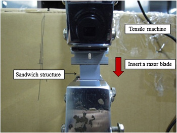
For the peeling-induced splitting process, a razor blade was pushed into the middle of the sandwiched structure to initiate a crack, as shown in Fig. 1. MTS Insight 100 with the minimum test speed of 0.01 mm/min (MTS Systems Corporation, Eden Prairie, Minnesota, US) was used to push the razor at a speed of 0.01 mm/s during the splitting of the polymer film, using the displacement control. All the splitting was performed at 25 °C.
Peeling-induced splitting of a PMMA-based film by pushing a razor blade into a sandwich structure.

Optical imaging was performed on a BX-51 optical microscope (Olympus Optical Co., Shinjuku-ku, Tokyo, Japan) equipped with a DFK51AU02 CCD camera (Imaging Source, Bremen, Germany) under the reflection mode. Optical images were analyzed, using the software ImageJ (National Institute of Health, Bethesda, MD, USA).
A Brucker Dimension Icon AFM (Santa Barbara, CA, USA) was used to measure the spatial wave length and amplitude of the surface gratings formed on the PMMA-based films. All measurements were conducted under the tapping mode, using silicon scanning probes, PPP-NCHR (Nanosensors, Neuchatel, Switzerland). The nominal spring constant and resonance frequency of the PPP-NCHR were 42 N/m and 330 kHz, respectively. AFM images were analyzed, using Nanoscope Analysis software (Santa Barbara, CA, USA).
III. RESULTS AND DISCUSSION
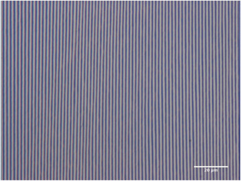
Figure 2 shows a typical optical image of the surface structure created on a PMMA-based film of 514 ± 1.7 nm in thickness by the peeling-induced splitting process. The surface structure exhibits parallel grating in accord with the observation by Pease III et al. Reference Pease, Deshpande, Wang, Russel and Chou15 As suggested by Freund, Reference Freund21 the formation of the surface grating is associated with the crack propagation in the film induced by the tensile stress. In general, the crack propagation will lead to the formation of ripples perpendicular to the direction of the crack propagation, which is dependent on the state of local stress. Slight change in the state of local stress can change the crack path, which likely will lead to the variation of the orientation of the ripples.
Surface structures created by the peeling-induced splitting of a nonirradiated PMMA-based film of 514 ± 1.7 nm thickness.

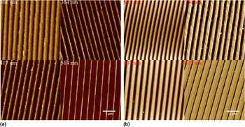
Figure 3 shows AFM images of the surface gratings created by the peeling-induced splitting of the PMMA-based films of various thicknesses with and without the UV irradiation where the film thickness is shown at upper-left corner of each figure. In general, there is no significant effect of the UV irradiation on the topology of the surface gratings. The wave length of the surface gratings increases with the increasing film thickness. Such behavior suggests that there exist smaller residual stresses in thicker films than thinner films. The residual surface stresses introduce surface instability, resulting in the formation of periodic structures with larger wavelengths in thicker polymer films.
AFM images of the surface gratings created by the peeling-induced splitting of (a) nonirradiated PMMA-based films, and (b) UV-irradiated PMMA-based films with a dose of 4 J/cm2.

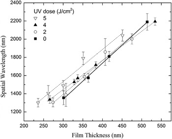
From the AFM images, one can determine the spatial frequency and amplitude of the corresponding surface gratings. Figure 4 shows the variation of the spatial wave length of the surface gratings with film thickness for four different UV doses. Similar to the peeling-induced splitting of the polymer films after exposing to gamma-irradiation, Reference Lee, Yang, Chen and Lee17 the spatial wave length is a linear function of the film thickness for the experimental conditions, independent of the UV doses used. Using curve-fitting to fit the experimental data, one obtains
 $${\lambda _0} = \left( {3.96 \pm 0.1} \right)h + 152.82$$
 $${\lambda _2} = \left( {3.7 \pm 0.31} \right)h + 285.12$$
 $${\lambda _4} = \left( {3.2 \pm 0.03} \right)h + 485.47$$
 $${\lambda _5} = \left( {3.53 \pm 0.31} \right)h + 475.28$$
in which λ is the spatial wave length, h is the film thickness, and the subscript represents the UV dose with the unit of J/cm2 used in the UV irradiation. The units of both λ and h are nm. The slope decreases with the increasing UV dose for the UV dose less than or equal to 4 J/cm2, while, for the UV dose of 5 J/cm2, the slope is larger than that with the UV dose of 4 J/cm2. The mechanism for such behavior is unclear. It might be associated with the structural change in the PMMA-based films under the UV irradiation. The slopes as given in Eqs. (1)–(4) are in the range of 3.2–3.96, less than 4.95-6.72 for the surface patterns formed on the surface of the PMMA-based films after exposing to gamma-irradiation in air. Reference Lee, Yang, Chen and Lee17 Such a difference suggests that the PMMA-based films after the UV irradiation possessed different structures from those after the gamma-ray irradiation.
Variation of spatial wave length on film thickness for the surface gratings on the PMMA-based films irradiated with several UV doses (dose rate: 1.35 mW/cm2).

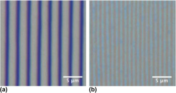
It needs to point out that further increase in the UV dose makes it more difficult to construct surface gratings with consistent geometrical characteristics. Figure 5 shows two optical images of the surface gratings formed on the PMMA-based films of 505 ± 1.3 nm in thickness with a UV dose of 6 J/cm2. Periodic surface structures are observed for both films, while the spatial wavelengths of these two films are significantly different. This result suggests that the UV irradiation of high doses likely introduces significant changes in the microstructures of the polymer films, leading to the abnormality in the formation of surface structures. For the PMMA-based films under the UV irradiation with a dose of 10 J/cm2, there are no ripple patterns presented on the surface of the PMMA-based films. Thus, one can conclude that the UV irradiation with a dose over 6 J/cm2 reduces the probability to create ripple patterns on the same scale as those with doses less than 6 J/cm2.
Optical images of the surface gratings formed on PMMA-based films of 505 nm in thickness with a UV dose of 6 J/cm2, showing significant difference in the spatial wave length; (a) 2680 nm, and (b) 1160 nm.

Lin et al. Reference Lin, Yang and Lee13 and Liang et al. Reference Liang, Yang and Lee14 suggested that the formation of surface structures on polymer films is controlled by surface stress and introduced the concept of residual surface stress. For a surface grating formed on a polymer film of thickness h, the relationship between the apparent surface stress, k, and the spatial frequency, ω (2π/spatial wave length), can be expressed as Reference Lin, Yang and Lee13
 $$k = {{\sqrt 2 E\left[ {5 - 12\nu + 8{\nu ^2} + 4{h^2}{\omega ^2} + \left( {3 - 4\nu } \right)\cosh \left( {2\sqrt 2 h\omega } \right)} \right]} \over {4\left( {1 - \nu } \right)\left( {1 + \nu } \right)\omega \left[ {2\sqrt 2 h\omega - \left( {3 - 4\nu } \right)\sinh \left( {2\sqrt 2 h\omega } \right)} \right]}}\quad ,$$
where ω is the spatial frequency, E is Young's modulus of the polymer film, and ν is Poisson's ratio. Note that k can be calculated from the surface energy, γ, and the residual surface stress, σ, as
 $$k = \gamma + \sigma \quad ,$$
where σ is a function of spatial frequency, ω (=2π/λ) and the film thickness, h. From Eq. (5), one can calculate the apparent surface force, f, applied on the polymer film as
 $$f = kh\quad .$$
Using E = 4.9 GPa and v = 0.39 for the mr-I8030E PMMA-based photoresist, Reference Huang, Lou, Tsai, Tung-Chuan and Lin22 one can calculate the apparent surface stress introduced by the splitting of the polymer films and the apparent surface force. Figure 6 shows the variations of the apparent surface stress and apparent surface force with film thickness for the PMMA-based films subjected to the UV irradiations of 3 different UV doses. For comparison, the results for the PMMA-based films without the UV irradiation are also included in Fig. 6. All of the surface stresses are negative, indicating that the separation of the PMMA-based films by the peeling-splitting process introduces compressive stresses on the surface of the PMMA-based films. The magnitude of the apparent surface stress generally increases with the increasing film thickness.
Thickness effect on the apparent surface stress and apparent surface force on the polymer films subjected to the UV irradiations of 3 different UV doses; (a) surface stress, and (b) surface force.

It is interesting to note that the magnitude of the apparent surface force is approximately a linear function of the film thickness, as shown in Fig. 6(b). The slope decreases with the increasing UV dose for the UV dose less than or equal to 4 J/cm2, while, for the UV dose of 5 J/cm2, the slope is larger than that with the UV dose of 4 J/cm2. This result again reveals that the UV irradiation likely introduces the change in microstructures of the PMMA-based films. There likely exists the embrittlement of the polymer films induced by photodegradation.
As shown in Eq. (6), the apparent surface stress consists of two components: residual surface stress and surface energy. To examine the effect of the UV irradiation on surface energy and the contribution of the surface energy to the apparent surface stress, the surface energy of the irradiated PMMA-based films was determined. According to the Owens–Wendt method, Reference Owens and Wendt23 the surface energies of liquid and solid can be expressed as the sum of dispersive and polar components, i.e.,
 $${\gamma _{\rm{sv}}} = \gamma _{{\rm{sv}}}^{\rm{d}} + \gamma _{{\rm{sv}}}^{\rm{p}}$$
and the relationship between the contact angle, θ, and the surface energies of both liquid and solid is
 $${\gamma _{{\rm{lv}}}}\left( {1 + \cos \,\theta } \right) = 2\sqrt {\gamma _{{\rm{lv}}}^{\rm{p}}\gamma _{{\rm{sv}}}^{\rm{p}}} + 2\sqrt {\gamma _{{\rm{lv}}}^{\rm{d}}\gamma _{{\rm{sv}}}^{\rm{d}}} \quad .$$
Here, γlv and γsv are the surface energies of liquid and solid, respectively. The superscripts d and p represent the dispersive and polar components, respectively.
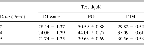
Using a FTA 125 contact angle instrument (First Ten Angstroms Inc., Portsmouth, VA, USA), the contact angles of three different liquids on the irradiated PMMA-based films were measured. Table I lists the contact angles of three test liquids on the PMMA-based films irradiated with the doses of 2, 4 and 5 J/cm2.
Contact angles of three test liquids on the irradiated PMMA-based films.

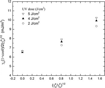
Figure 7 shows the variation of the parameter of
 ${{{\gamma _{{\rm{lv}}}}\left( {1 + \cos \,\theta } \right)}/ \mathord{\left {\vphantom {{{\gamma _{{\rm{lv}}}}\left( {1 + \cos \,\theta } \right)} {2\sqrt {\gamma _{{\rm{lv}}}^{\rm{d}}} }}} \right. \kern-\nulldelimiterspace} {2\sqrt {\gamma _{{\rm{lv}}}^{\rm{d}}} }}$
with
 $\sqrt {{{\gamma _{\rm{lv}}^{\rm{p}}/ \mathord{\left {\vphantom {{\gamma _{lv}^p} {\gamma _{{\rm{lv}}}^{\rm{d}}}}} \right. \kern-\nulldelimiterspace} {\gamma _{{\rm{lv}}}^{\rm{d}}}}}$
. It is evident that the contact angles of the three liquids decreases with increasing the UV dose. This result suggests that the UV irradiation causes the change of the microstructures in the PMMA-based films, as revealed from the change of the slope of the apparent surface force to the film thickness. Using the values of
 $\gamma _{{\rm{lv}}}^{\rm{d}}$
and
 $\gamma _{{\rm{lv}}}^{\rm{p}}$
and the curve-fitting of Eq. (9), the surface energy of the irradiated PMMA-based films were determined and listed in Table II. The magnitudes of the surface energies are six orders smaller than the surface stresses in Fig. 5(b). The surface energy plays a much less important role in controlling the formation of the surface gratings. It is the compressive-residual surface stress that determines the formation of the surface gratings.
Surface energy of the PMMA-based films irradiated with doses of 2, 4, and 5 J/cm2.

Surface energies of the PMMA-based films irradiated with various UV doses.

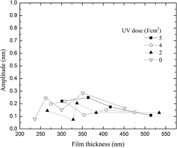
Figure 8 shows the variation of the amplitude of the surface gratings with film thickness for the PMMA-based films exposed to various UV doses. All the surface gratings have amplitudes approximately in the same range. There is a larger scattering of the amplitudes of the surface gratings formed on the irradiated PMMA-based films than that of the surface gratings formed on the non-irradiated PMMA-based films. It is known that the amplitude of a surface grating is associated with the ratio of the energy per unit volume stored in the surface grating to the mechanical work per unit volume done by the splitting process. Reference Lin, Yang and Lee13,Reference Liang, Yang and Lee14 The result of all the amplitudes being approximately in the same range suggests that the peeling-induced formation of surface gratings is only dependent on local deformation state (zone) near the propagation front, on which the confinement effect of the Si plates is limited for the film thicknesses used. The deformation zone affecting the peeling-induced splitting likely is much smaller than the smallest thickness of ∼236 nm.
Variation of the amplitude of the surface gratings with film thickness for various UV doses.

IV. SUMMARY
Understanding environmental effect on the formation of surface structures on the surface of soft matter will help to improve the reliability and performance of flexible electronics, photonics, microfluidics, etc. The effect of the UV irradiation was investigated on the peeling-induced formation of surface gratings on the PMMA-based polymer (nanoimprint photoresist) films. The spatial wave length is a linear function of the film thickness for the experimental conditions, independent of the UV doses used. The slope decreases with the increasing UV dose for the UV dose less than or equal to 4 J/cm2, while, for the UV dose of 5 J/cm2, the slope is larger than that with the UV dose of 4 J/cm2. The peeling-splitting process introduces compressive stresses on the surface of the PMMA-based films, which are much larger than the corresponding surface energies. The magnitude of the apparent surface force increases with the increasing film thickness. All the surface gratings formed have amplitudes approximately in the same range. For polymer films exposed to the UV irradiation with dose more than or equal to 10 J/cm2, the experimental results show that the peeling-induced splitting hardly produces any surface pattern on the surface of the polymer films and no periodic surface structures could be formed.
ACKNOWLEDGMENT
We are grateful for the Ministry of Science and Technology, Taiwan for financial support.