I. INTRODUCTION
Since the stability of graphene was demonstrated under an ambient condition in 2004 [Reference Novoselov1], the research community has been attracted by its potential high carrier mobility even at room temperature [Reference Novoselov1–Reference Bolotin3]. Actually, graphene appears as a promising candidate for the fabrication of the future generation of high-frequency electronic devices, in particular, for field-effect transistors (FET) [Reference Novoselov1, Reference Liao4–Reference Xia, Farmer, Lin and Avouris12]. One of the main advantages of graphene for this kind of application comes from its planar structure, which allows the use of well-matured planar processes in the semiconductor industry. Several research results focused on the static characterization of graphene-based transistors are available in the literature [Reference Zhu and Woo7–Reference Xia, Farmer, Lin and Avouris12]. However, studies in the high-frequency domain are still lacking [Reference Liao4–Reference Meric, Baklitskaya, Kim and Shepard6]. We present a study dedicated to the fabrication and characterization of graphene-based field-effect transistor for high-frequency applications.
II. GRAPHENE SYNTHESIS AND CHARACTERIZATION
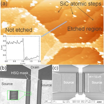
There are different ways to synthesize graphene [Reference Novoselov1, Reference Forbeaux, Themlin and Debever13–Reference Cao17]. In this work, thermal decomposition on axis SiC-4H {0001} substrate is considered [Reference Berger14, Reference Rollings15]. In order to achieve graphene layer of high quality, an exposure of SiC substrate to a silicon flux during 1 h at 1100°C is used to obtain a high-quality SiC surface [Reference Ferrer, Fernandez, Moreau, Vignaud, Godey and Wallart18]. Based on the parameters of graphitization (6 min at 1400°C), the multilayer of graphene is realized. The layer number is deduced from Atomic Force Microscopy (AFM) measurements of the active layer's total thickness (1.66 nm) (Fig. 1(a)) after selective etching of graphene versus the SiC substrate: the oxygen plasma etching is used. By assuming that the inter-distance between two layers is 0.335 nm, the estimated number of graphene layers is 5. The total thickness is measured on the same atomic step (Fig. 1(a)) in order to improve the result accuracy. Transport properties of the active layer are determined from the Hall effect measurement. Mobility of 427 cm2/V s and carriers density (electrons) of −7.5 × 10¹³ are obtained.
(a) Measurement of grapheme-layer thickness by AFM. On the same SiC atomic step, the height measured is 1.66 nm, which results about five monolayers of graphene. (b) Scanning electron microscopy (SEM) images of e-beam mask showing arrays of ribbons (50 nm width, and 50 nm spaced). (c) SEM image of final device.

III. DEVICE FABRICATION AND CHARACTERIZATION
A) Device fabrication
Graphene nanoribbon field-effect transistors (GNRFET) considered in this work is a dual gate device, in a coplanar access structure. GNR arrays are defined by e-beam lithography with a ribbon width of 50 nm, 50 nm spaced (Fig. 1(b)). The Al2O3 gate oxide on GNR is obtained by two steps of oxidation of thin aluminum films deposited by e-beam evaporation. To this end, about 2 nm of aluminum is evaporated before exposure in air during 4 h. This process, repeated twice, leads to a final Al2O3 thickness of 5 nm. The top gate (Ni/Au 50 nm/300 nm) is finally deposited by lift-off process. The gate length is Lg = 150 nm, and the gate width is W = 12 µm (Fig. 1(c)). Therefore, there are 120 GNRs per gate channel.
B) Device characterization
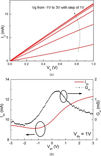
DC and HF characterization of our GNRFET are performed using an Agilent E8361A network analyzer (VNA). In the DC regime, at Vds = 1 V, a drive current (Ids) of 12.5 mA, and Gm of 1.47 mS are obtained (Fig. 2). Asymmetrical ambipolar effect is observed (Fig. 2(b)) because of the presence of high electron density in the multilayer of graphene.
(a) DC output characteristics (device drain current Ids versus drain voltage Vds at different gate voltage Vgs). (b) Transfer characteristics (Ids versus Vgs) of the device, Dirac point is at Vgs = −0.8 V; and transconductance Gm as a function of Vgs, at Vgs = 0.8 V, Gm_max = 1.45 mS is obtained.

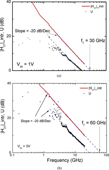
HF characterization is performed from 10 MHz to 20 GHz. A common Line-reflect-match calibration procedure is used. In order to investigate the intrinsic HF characteristics of our GNRFET, a special “open” structure is fabricated on wafer by means of the same process used for the active device. This “open” structure is exactly the same as our GNRFET except there is no graphene between the source and the drain region. The de-embedded procedure is similar to the one described in [Reference Nougaret19]. The intrinsic current gain cut-off frequency (fT) of 30 GHz and maximum oscillation frequency (f max) of 17 GHz (Fig. 3(a)) were obtained at Vds = 1 V and Vgs = −0.8 V.
(a) Intrinsic current gain (|H 21|_intr) and unilateral gain (U) under bias of Vds = 1 V. The best intrinsic fT of 30 GHz and fmax of 17 GHz are obtained. (b) Under the bias of Vds = 3 V, fT = 60 GHz, and fmax = 28 GHz have been measured.

We have also investigated the impact of Vds on the HF performance of our GNRFET. For the same device, better fT (60 GHz) and fmax (28 GHz) (Fig. 3(b)) were obtained when increasing Vds from 1 to 3 V. This can be partially explained by the rise of Gm from 1.47 to 4.05 mS, knowing that fT can be approximately estimated by the expression Gm/(2πCgs).
IV. CONCLUSION
In conclusion, multilayered graphene on SiC is used to fabricate field-effect transistors. The active layer shows high carrier density and low mobility. The use of array of nanoribbons helps to improve the gap of graphene layers and to achieve a high DC current. Analysis of high-frequency performance shows that despite the relatively low on/off current ratio, the intrinsic current gain cut-off frequency of 60 GHz, associated to a maximum frequency of oscillation of 28 GHz are obtained. Most importantly, this work shows that using GNR is another way to improve high-frequency performance of graphene multilayered devices.
 Nan Meng received his masters degree in Microelectronic and Nano Technology in University of Sciences and Technologies of Lille, France in 2007. He is actually working toward the Ph.D. degree at Institute of Electronics, Microelectronics and Nanotechnology. He joined the research group of Henri Happy at IEMN where he participates in the design, fabrication, and characterization of Graphene nano ribbon FET.
 Francsico-Javier Ferrer received his Ph.D. degree in physics from the University of Seville (Spain), in 2007. Until 2008 he was working on mixed oxides thin films in National Center for Accelerators (CSIC, Spain) and Institute for Materials Science of Seville (CSIC, Spain). Following this period, he joined the Epiphy group in the Institut d'Electronique, de Microélectronique et de Nanotechnologie (CNRS, France) where he worked on the synthesis of epitaxial graphene by SiC graphitization.
 Dominique Vignaud obtained his Ph.D. in 1983 and the “Thèse d'Etat” in 1989, both from the University of Lille, for works on the optical properties of plastically deformed III–V compounds (InSb and GaAs). He was hired by the CNRS in 1983. He joined the Institute of Electronics, Microelectronics and Nanotechnology (IEMN) in 1999, where he has achieved studies of the optical properties of III–V heterostructures. His current interest stands in the elaboration and characterization of epitaxial graphene.
 Gilles Dambrine received his Ph.D. and Habilitation à Diriger des Recherches en Sciences degrees from the Centre Hyperfréquences et Semiconducteurs, University of Lille, Lille, France, in 1989 and 1996, respectively. He is currently a Professor of Electronics with the University of Lille and the Head of Institute of Electronics, Microelectronics and Nanotechnology, Villeneuve d'Ascq Cedex, France. His main research interests are concerned with the modeling and characterization of ultimate low-noise devices for application in millimeter and sub-millimeter-wave ranges. Over these few years, his research interests are oriented to the study of the microwave and millimeter-wave properties and applications of advanced silicon devices. Dr. Dambrine is currently a Reviewer in various IEEE transactions and a member of the Technical Program Committee of the European Microwave Integrated Circuits and the European Solid-State Device Research Conference conferences.
 Henri Happy received the Ph.D. degree from the University of Lille, Lille, France, in 1992. In 1998, he joined the Institute of Electronics, Microelectronics and Nanotechnology (IEMN), University of Lille. He is currently a Professor of Electronics with the University of Lille. His first research interests are concerned with high electron-mobility transistor (HEMT) modeling using a quasi-two-dimensional (2-D) approach. He is currently involved in the design and realization of monolithic microwave-integrated circuits (MMICs) for optical communications systems using either planar or three-dimensional (3-D) topologies. He is one of the principal designers of the software HELENA. He coauthored HELENA for HEMT Electrical Properties and Noise Analysis (Norwood, MA: Artech House, 1995). His current research is concerned with fabrication and HF characterization of nanometer devices.