I. INTRODUCTION
The availability of a scalable process for the fabrication of uniform GaN nanowiresReference Hersee, Sun and Wang1 has created a realistic opportunity for GaN nanowire-based devices to transition from the research laboratory into production. This process does not employ potentially contaminating metal catalystsReference Yoo, Hong, An, Yi, Chon, Joo, Kim and Lee2 and uses only high-purity metalorganic and ammonia precursors that are typical of regular metalorganic chemical vapor deposition (MOCVD). The electrical properties of GaN nanowires grown with this process were shown to be well behaved.Reference Talin, Leonard, Swartzentruber, Wang and Hersee3, Reference Talin, Swartzentruber, Leonard, Wang and Hersee4 Highly doped GaN nanowires exhibited Ohmic conduction, whereas low-doped or undoped nanowires exhibited space charge-limited conduction, and an electron mobility of 386 cm2/V·s was extracted from the conductivity data.Reference Yoo, Hong, An, Yi, Chon, Joo, Kim and Lee2 The nanowires exhibited an intense photoluminescence (PL) signal,Reference Hersee, Sun and Wang1 and lasing was observed when the nanowires were optically pumped at high intensity.5 Transmission electron microscopy (TEM) analysis shows that even though threading defects are ubiquitous in planar GaN layers, they are absent from the GaN nanowires.Reference Hersee, Sun and Wang1, Reference Kavanagh6 HomojunctionReference Kim7, Reference Hersee, Fairchild, Rishinaramangalam, Ferdous, Zhang, Varangis, Swartzentruber and Talin8 and heterojunctionReference Kishino, Kikuchi, Sekiguchi and Ishizawa9 GaN light-emitting diodes (LEDs) based on nanowires have been reported. Three-dimensional nanostructures presenting { } sidewalls, as reported here, are especially interesting as they offer a potential route to the fabrication of defect-free, nonpolar LEDs.
The elimination of TDs in GaN is important for an LED because this is expected to reduce the LED reverse bias leakageReference Ferdous, Wang, Fairchild and Hersee10 and to improve the longevity, especially in those devices that operate at high power.Reference Mukai, Takekawa and Nakamura11 Furthermore, it remains to be seen if the reduction of internal quantum efficiency of LED at high current density (i.e., the “droop” issue) will be improved by reducing the TD density to zero.
II. EXPERIMENTAL DETAILS AND RESULTS
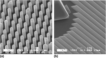
The pulsed MOCVD nanowire process used hereReference Hersee, Sun and Wang1 yields GaN nanowires with a [0001] direction that are bounded by six { } atomically smooth sidewalls. The nanowires are selectively grown through a 30-nm silicon nitride growth template that was patterned by interferometric lithographyReference Brueck12 and reactive ion etching. The silicon nitride growth template was deposited onto an underlying [0001] GaN planar film that was previously grown by regular MOCVD on a sapphire substrate. The cross-sectional geometry of the nanostructures is controlled by the shape of the apertures in the growth template. Nanowire and nanowall structures [Figs. 1(a) and 1(b)] can be produced by appropriately shaping the apertures in the growth template. The vertical extent of the GaN nanostructures in the [0001] direction is controlled by the growth duration.
Scanning electron microscopy (SEM) images showing GaN nanostructures fabricated by the pulsed metalorganic chemical vapor deposition process described in Ref. Reference Hersee, Sun and Wang1; (a) GaN nanowires and (b) GaN nanowalls.

Previous cross-sectional transmission electron microscopy (XTEM) analysis of GaN nanowire arrays showedReference Hersee, Sun and Wang1 that threading dislocations were absent from the nanowires even though the TD density in the planar GaN layer, beneath the GaN nanowires, was measuredReference Ferdous, Sun, Wang, Fairchild and Hersee13 to be between 108 and 109 cm−2. TDs can only propagate where a nanowire connects epitaxially to the underlying GaN planar layer. In the absence of other defect elimination or creation mechanisms, the TD density within the GaN nanowires would, therefore, be expected to replicate the TD density observed in the underlying GaN layer. The authors of this study have so far examined the XTEM images of more than 100 nanowires, representing a total nanowire cross-section area of ∼10−5 cm−2. If the TD density inside the nanowires had remained at the same value as in the underlying planar GaN film, then we should have observed between 1000 and 10,000 TDs inside the nanowires. In fact, TDs were observed to enter a nanowire on less than 10 occasions. This represents an average TD density inside the nanowires of ∼106 cm−2, which corresponds to the lower detection limit of XTEM for dislocation density measurement. We, therefore, conclude that an additional defect elimination mechanism is active in these nanostructures.
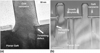
The nature of this additional defect reduction mechanism is revealed by bright-field XTEM in Fig. 2, which shows two examples of a selectively grown nanostructure, the growth template, and the underlying planar GaN. In Fig. 2(a), a threading dislocation (see arrow) bends toward the { } nanowire sidewall at the interface between the GaN nanowire and the underlying planar GaN. Figure 2(b) gives a second example of this bending and termination behavior, where in this case the bending occurs after the TD has extended ∼100 nm into the nanowire. In both examples, after bending and termination has occurred, the subsequently grown GaN nanowire is defect free. The bending of threading defects from their normal c-orientation toward a sidewall surface has been observed previously during the initial stage of epitaxial lateral overgrowth (ELO) of GaN on (111) silicon.Reference Tanaka, Kawaguchi, Sawaki, Hibino and Hiramatsu14 During ELO, however, when the adjacent islands meet and coalesce,Reference Béré and Serra15 the sidewall is eliminated and the threading defects reorient toward the c-direction.
Cross-sectional transmission electron microscopy (XTEM) images showing (a) TD bending and termination at the interface between a nanowire and the underlying planar GaN film and (b) TD bending and termination after initial entry into the GaN nanowire.

In the uncoalesced nanostructures discussed here, the TD bending and termination process is highly efficient as the sidewall remains in existence. The result is that the vast majority of GaN nanowires examined by TEM do not contain TDs, even though they are epitaxially connected to an underlying GaN layer that has a high TD density in the range of 108–109 cm−2. It is known that a dislocation (just like any physical system) will attempt to minimize its free energy, and it is also known that the dislocation energy will grow in proportion to its line lengthReference Béré and Serra15, Reference Elsner, Jones, Sitch, Porezag, Elstner, Frauenheim, Heggie, Öberg and Briddon16. We, therefore, propose that the driving force for this TD elimination process is the reduction of the dislocation line energy, which occurs when the dislocation shortens its length by terminating at a nanowire sidewall instead of continuing to propagate vertically in the [0001] direction. This energy reduction can be significant as the line energy for an edge dislocationReference Elsner, Jones, Sitch, Porezag, Elstner, Frauenheim, Heggie, Öberg and Briddon16 in GaN is 2.2 eV/Å, whereas the line energy for a [0001] screw dislocationReference Yong, Soh, Zhang, Chow and Chua17 in GaN is between 3 and 5 eV/Å.
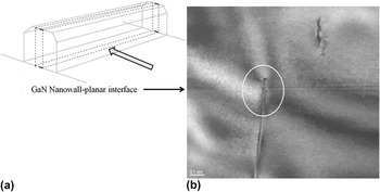
The TD bending process was also observed in nanowall structures as shown in Fig. 3. Figure 3(a) shows the position of the thinned XTEM sample along the length of the nanowall and the direction of XTEM viewing of this sample (arrow). Figure 3(b) shows a bright-field XTEM image of this sample, where a TD is observed to terminate at the interface between the nanowall and the planar GaN layer [see circle in Fig. 3(b)]. Crystallographic theory indicates that the termination of a TD inside any crystal is not possible, so we interpret this apparent termination as due to the bending of the TD toward a sidewall facet that is either behind or in front of the plane of the thinned XTEM sample.
XTEM micrographs showing (a) the orientation of the XTEM sample with respect to the GaN nanowall and (b) the apparent termination (circled) of a TD at the interface between the nanowall and the underlying planar GaN.

III. ANALYSIS
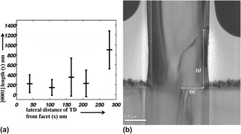
Figure 4(a) plots the vertical [0001] length of the TD as a function of the lateral distance between the TD and the nearest sidewall facet. Figure 4(b) is an XTEM micrograph on which the vertical [0001] length of the TD (y) and the lateral distance between the TD and the nearest sidewall facet (x) are defined. During lateral movement, the TD may also be moving forward toward the front of the thinned TEM sample or toward the back of the TEM sample. The parameter “x” in Fig. 4(a) is, therefore, the projection of the lateral trajectory of the TD onto the [ ] direction. Although there is significant scatter in this data, due to the small number of these “rare” observations, it appears that a correlation exists and the vertical extent of the TD is greater when the TD is farther from a sidewall facet.
(a) A plot showing the correlation of the [0001] length of the TD (y), with the lateral distance from the nanostructure sidewall surface (x). Note: “x” is the projection of the lateral trajectory of the TD onto the [ ] direction. (b) XTEM micrograph showing the definition of TD [0001] length (y) and lateral distance from the sidewall facet (x).

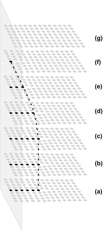
A natural question is “does the TD convert to another type of defect as it bends toward a sidewall and terminates?” The simple model shown schematically in Fig. 5 indicates that conversion is not required.
An illustration of the climb of a pure-edge dislocation toward a nanowire facet, followed by termination at that facet. (For simplicity, this model is shown for a simple cubic, mono-elemental crystal.)

Threading dislocations in GaN are line defects typically with either edge or screw component, or both components, and an approximately [0001] line direction. For simplicity in Fig. 5, the TD is shown as a pure-edge dislocation in a mono-elemental, simple cubic lattice. We consider the vertical length (a to b) of a TD that has entered the nanowire from an underlying planar layer and is seven atomic spacings from the sidewall facet. Both the growth direction and the TD line direction are in the vertical direction. As growth proceeds vertically (c thru f), the dislocation moves left toward the nanowire sidewall by climb, under the influence of the image force from the sidewall facet. Eventually, this threading defect intercepts the sidewall surface and terminates. In the general case of a TD that contains edge and screw components, this dislocation bending and termination process will involve climb and glide.
These GaN nanostructures offer nonpolar, { } sidewalls that can be used as substrates for the subsequent growth of heterostructure LEDs. For the reasons described earlier, it is important to determine if additional defects are created when LED heterostructures are grown onto these {
 } sidewalls. Our XTEM study of heterojunction growth onto these {
 } sidewalls is preliminary; however, the results presented below represent the typical behavior that has been so far observed on a more limited set of XTEM samples.
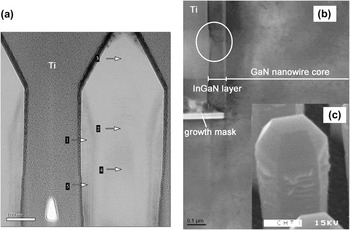
Figure 6(a) shows a bright-field XTEM micrograph of a GaN–AlGaN heterojunction comprising a shell of ∼50 nm of Al0.1Ga0.9N grown coaxially around a 300-nm-diameter GaN nanowire core. The structures were infilled with titanium, and then thinned from two sides to ∼500 Å using standard focused ion beam (FIB) processing.
(a) XTEM micrograph showing the growth of an AlGaN shell around a central GaN nanowire core. As determined by energy-dispersive x-ray spectroscopy analysis of the XTEM sample, regions 1, 3, and 5 are AlGaN, whereas regions 2 and 4 are GaN. (b) XTEM micrograph showing the growth of an InGaN shell around a central GaN nanowire core. Indicated on the figure are the edge of the SiNx growth mask on the left, the GaN core on the right, and the InGaN layer that grows laterally on the sidewall above the growth mask. The circled area shows a crater in the InGaN layer. (c) SEM micrograph for the sample shown in (b) before focused ion beam thinning. This image shows the roughening of the nanowire sidewall surfaces that generally occurs when InGaN is grown around the central GaN core.

Based on the limited XTEM analysis that has been completed to date (∼20 nanowires have been studied by XTEM), it appears that no new defects are created inside the nanostructure during the deposition of a GaN–AlGaN heterojunction. The nonpolar, { } sidewall facet remains predominant although some terracing is observed on these sidewalls, and this gives rise to an apparent tapering of the nanowire. Scanning electron microscopy (SEM) analysis of the sidewalls on a much larger set of GaN–AlGaN heterojunction nanowires confirms that the {
 } sidewalls remain smooth. Also, less terracing (that produces an apparent taper on the sidewall) was observed when the nanowire array pitch was increased.
Preliminary XTEM data of a GaN–InGaN heterojunction consisting of a shell of ∼50 nm of In0.07Ga0.93N grown coaxially around a 300-nm-diameter GaN nanowire core are shown in Fig. 6(b). The InGaN composition was estimated using room temperature PL. A standard FIB thinning procedure was again used to prepare the XTEM samples, and ∼10 nanowires were studied. Figure 6(b) shows the edge of the left side of one nanowire in the vicinity of the growth mask. The edge of the SiNx growth mask is at the left, the GaN core is on the right, and the InGaN layer can be observed to grow laterally on the sidewall above the growth mask. Figure 6(c), shown as an inset in Fig. 6(b), is the SEM micrograph for the sample shown in Fig. 6(b) taken before XTEM sample preparation.
SEM analysis [Fig. 6(c)] reveals a nonsmooth nanowire sidewall surface that is decorated with noncrystalline ridges. These sidewall ridge deposits are not directly observable after XTEM sample preparation; however, they are replaced by craters in the InGaN layer. One such crater is circled in Fig. 6(b). A basal plane (c-plane) defect can also be resolved at the tip of this crater, and this defect does not appear to propagate from the InGaN layer into the GaN nanowire core. Although these craters have an approximate v-shape, their axis is perpendicular to the [0001] direction and they are, therefore, not the well-known V-defects that are induced by threading dislocations and have an axis in the [0001] directionReference Yong, Soh, Zhang, Chow and Chua17.
Our preliminary hypothesis, that requires further verification, is that during InGaN core–shell growth on the nanowire sidewalls, indium segregates to the surface of the nanowire { } sidewall to create indium-rich “deposits” that roughen the sidewall surface [Fig. 6(c)]. During XTEM sample preparation, these indium-rich deposits are preferentially sputtered away leaving behind craters in the InGaN layer, shown as circled region in Fig. 6(b).
IV. CONCLUSIONS
In conclusion, a process for the elimination of threading dislocations in GaN nanostructures has been analyzed by XTEM. This elimination process appears to be extremely efficient when the TD is within 500 nm of the sidewall facet of the nanostructures. This TD elimination process also occurs in nanowall structures, where at least two out of six nanowall sidewall facets can be within close proximity to a TD. As the lateral dimension of the nanostructure increases, this TD elimination process becomes less efficient and nonzero TD densities are expected.
Preliminary results indicate that AlGaN and InGaN ternary alloys, as required for the fabrication of LEDs, can be grown onto the nonpolar, { } sidewall planes of the nanostructure. Further improvement of the InGaN growth morphology is required and is the focus of ongoing work.
ACKNOWLEDGMENT
This work was supported in part by the National Science Foundation Smart Lighting Engineering Research Center (No. EEC-0812056).