Introduction
Wireless communication systems have seen manifold developments with the introduction of multifunctional and multiband handheld portable devices in recent years and these devices demand antennas, with real time-dynamically adjustable and reversible characteristics [Reference Ojaroudi Parchin, Jahanbakhsh Basherlou, Al-Yasir, Abdulkhaleq and Abd-Alhameed1]. Reconfigurable patch antenna can satisfy this necessity as they can offer, multiband operation along with adjustable radiation characteristics [Reference Tang, Ouedraogo, Rothwell, Diaz and Fuchi2–Reference Anantha, Merugu and Rao5]. Most modern handheld wireless devices (viz. smartphones, tablets etc.) operate in frequency bands, such as sub-6-GHz 5G N77/N78/N79 (3.3–4.2 GHz, 3.3–3.8 GHz, 4.4–5 GHz), WLAN (5.2 GHz, 5.8 GHz), and Wi-Fi 6E (5.925–6.425 GHz, 5.925–7.125 GHz) [Reference Azim, Meaze, Affandi, Alam, Aktar, Mia, Alam, Samsuzzaman and Islam6, Reference Verma, Kumar and Yadava7]. As these devices, require productive redistribution of dynamic frequency bandwidth, frequency reconfigurable patch antenna (FRPA) becomes a relevant choice [Reference Singh, Kumar Soni, Siddiqui and Mishra8, Reference Khan, Shah and Ullah9]. Among all the techniques [Reference Chiu, Li, Song and Murch10–Reference Che, Meng, Lyu and Wu13] investigated so far to achieve frequency reconfigurability, the electrical switching technique is the most widely adopted, where, radio frequency microelectromechanical systems (RF-MEMS) [Reference Deng, Gan, Wei, Gong and Guo14], PIN diodes [Reference Chen, Ye, Zhuo, Liu, Zhang, Zhang and Liu15, Reference Baruah and Bhattacharyya16], and varactors [Reference Boukarkar, Lin, Yu, Mei, Jiang and Yu17], are used, as switches at different positions of a patch antenna. Various slot structures, parasitic elements, and nested patches are also used with different switches in a patch antenna for frequency reconfiguration [Reference Erfani, Nourinia, Ghobadi, Niroo-Jazi and Denidni18–Reference Bhattacharjee, Jiang and Behdad21]. However, a combination of switches (e.g., PIN diodes) and slots, loaded over a patch antenna provides a wide band frequency reconfigurability [Reference Yang and Rahmat-Samii22].
A reconfigurable printed Bowtie antenna with the switchable rectangular slot is reported in [Reference Mansoul and Seddiki23] for Wi-Fi (2.45 GHz), WiMAX (3.5 GHz), and WLAN (5.8 GHz) applications. In [Reference Shah, Khan, Ullah and Flint24], a FRPA with the truncated ground plane is investigated for Wi-Fi (2.45 GHz), WiMAX (3.5 GHz), and WLAN (5.4 GHz) services. A multiband switchable antenna of overall size (40 × 35) mm2 is studied in [Reference Ullah, Ahmad, Khan and Flint25] for 3G Advanced (2.1 GHz), Wi-Fi (2.4 GHz), WiMAX (3.35 GHz), WiMAX (3.5 GHz), WLAN (5.28 GHz), and fixed Mobile Satellite Services (5.97 GHz). In [Reference Chattha, Hanif, Yang, Abbasi and Rana26], a compact FRPA with three PIN diodes along with DC bias lines is reported, which covers eight 4 G LTE frequency bands 0.9 GHz, 1.4 GHz, 1.5 GHz, 1.6 GHz, 1.7 GHz, 1.8 GHz, 2.6 GHz, 3.5 GHz, and WLAN band 2.5 GHz for cellular communication. In [Reference Jhang and Sun27], a triple-band antenna is reported for WLAN (2.4, 5.2, 5.8 GHz) and Wi-Fi 6E (5.925–7.125 GHz) applications. A hexagonal-shaped frequency reconfigurable antenna is investigated and reported in [Reference Ullah, Ullah, Ahmad, Khan, Ahmad, Habib, Albreem, Alsharif and Uthansakul28], which supports the Wi-Fi (2.45 GHz), sub-6-GHz N77 5G band (3.3 GHz), 3G advanced (2.1 GHz), and WiMAX (3.5 GHz) frequency bands for portable and handheld devices. In [Reference Subbaraj, Kanagasabai, Alsath, Palaniswamy, Kingsly, Kulandhaisamy, Shrivastav, Natarajan and Meiyalagan29], a reconfigurable patch antenna printed on RO4003C flexible substrate, with four varactors is reported. The antenna reconfigures the resonant frequency at 0.9, 2.4, 3.5, and 5.5 GHz, covering GSM, Wi-Fi, WiMAX, and WLAN. A monopole antenna with dual-band characteristics for ON state of the inserted optical switch is reported in [Reference Iqbal and Saraereh30] for Wi-Fi (2.45 GHz) and WLAN (5.4 GHz) applications. A frequency-agile antenna with five switches inserted on a tune stub is reported in [Reference Qi and Xu31] for sub-6-GHz N78 (3.5 GHz) and N79 (4.9 GHz) 5G frequency bands mobile communication. However, the antennas reported in [Reference Mansoul and Seddiki23, Reference Ullah, Ahmad, Khan and Flint25, Reference Ullah, Ullah, Ahmad, Khan, Ahmad, Habib, Albreem, Alsharif and Uthansakul28, Reference Qi and Xu31] have not used either practical switches or proper DC bias circuitry consisting inductors and capacitors to prevent the interference between DC and RF signal. A two-layer FRPA [Reference Jin, Deng, Yang, Xu and Liao32] using four PIN diode switches is investigated for WLAN (2.45 GHz) and sub-6-GHz N78 5G band (3.5 GHz) applications. A compact FRPA is reported in [Reference Saikia, Dutta and Borah33], in which two RF PIN diode switches are mounted on two asymmetric L-shaped slots for frequency reconfiguration at four scattered resonant frequencies. These frequencies cover the Wi-BAN (4.75 GHz), sub-6-GHz 5G (4.9 GHz), and WLAN (5.2 GHz) services. Although, many of the reported antenna designed for sub-6-GHz 5G bands cover WLAN and WiMAX bands, to the best knowledge of the authors, there has been diminutive work focusing on covering Wi-Fi 6E bands with the same FRPA.
Individual U-slot and L-slot, loaded over the radiating patch to achieve frequency reconfiguration are already reported in various articles [Reference Saikia, Dutta and Borah33–Reference Lai, Wu, Hsieh, Wang and Jeng35]. The incorporation of a U-slot structure in a patch radiator results a flat input resistance and linear input reactance across a wider bandwidth than a conventional patch antenna [Reference Yang, Kishk and Lee34], while L-slot loading offers dual-band operation and compactness [Reference Reddy and Bhattacharjee36]. To achieve a wide reconfigurable frequency span in a compact patch antenna, a novel arrangement of an asymmetric armed U-slot and a reversed L-slot are incorporated in the radiating patch. Three RF PIN diodes are mounted on inimitable positions, their orientation and positions are optimized with the help of Ansoft HFSS v 13.0. Six reconfigurable resonant frequencies are obtained for different reconfigurable modes which cover two continuous frequency bands from 4.21 to 5.43 GHz and 5.69 to 6.6 GHz. The proposed FRPA covers various wireless standards such as aeronautical radio navigation (4.3 GHz), sub-6-GHz N79 5G band (4.4–5 GHz), WLAN (5.2, 5.8 GHz) along with Wi-Fi 6E (5.925–6.425 GHz).
Antenna design and configuration
Antenna geometry
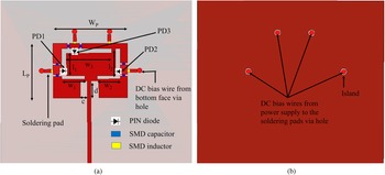
The proposed FRPA is synthesized on an FR4 substrate (εr = 4.4 and tanδ ~ 10−2, dimensions 35 × 40 × 1.6 mm3). The designed FRPA is shown in Fig. 1. Using the transmission line model (TLM) [Reference Balanis37], the base rectangular patch is designed at 6 GHz with length Lp = 11.59 mm and width Wp = 15.49 mm. Microstrip line feeding is adopted for RF excitation of the patch. The length and width of the inset feed line are 17.8 mm and 0.8 mm respectively. Optimization for the notch dimension in the inset feed is carried out using HFSS ver.13.0 and are found as c = 1.5 mm and d = 3.6 mm. A combination of an asymmetric armed U-slot and a reversed L-shaped slot are introduced on the base patch. To alter the electrical length of the patch and the surface current densities, so as to achieve frequency reconfigurability, three RF PIN diodes (PD1, PD2, and PD3) are inserted in the slots, which works as switches. The slot dimensions, orientation and PIN diode positions are also optimized to obtain a wide reconfigurable frequency band. Optimized physical dimension of the slots are found as l 1 = l 2 = 6.5 mm, w 1 = w 2 = 3.8 mm and w 3 = 10.4 mm. Width of the three rectangular arms of the etched slots (asymmetric armed U-slot and reversed L-shaped slot) in which PIN diodes are mounted is 1 mm while other two arms of each slot have a width of 0.7 mm. Six small rectangular shaped sections are etched near the PIN diodes to insert six DC block capacitors of DC bias network. Size of the rectangular portion etched near PD1 is (1.79 × 0.4) mm2, (1.5 × 0.4) mm2 for the PD2 while for PD3, it is (1.59 × 0.4) mm2. Four circular portions (islets) of diameter 1.4 mm are etched on the ground plane to insert the DC bias wires through the substrate and connect to the RF PIN diodes.
(a) Top view, (b) Bottom view of the FRPA.

DC biasing circuit
Three SMP 1345-040LF PIN diodes are used in the proposed FRPA as RF switch to obtain the desired frequency reconfigurability. Two of them are mounted on the asymmetric armed U-slot while the third one is inserted in the reversed L-slot as shown in Fig. 1(a). For simulation in HFSS, PIN diode is modeled with ON (forward bias) and OFF (reverse bias) state of a RLC equivalent circuit. The ON state of the PIN diode is obtained through a series connection of a resistance, Rs = 1.5 Ω and an inductance Ls = 0.7 nH in the RLC equivalent circuit. The OFF state equivalent circuit of PIN diode is designed by connecting an inductance of 0.7 nH in series with a capacitance of 0.19 pF.
The DC bias network, shown in Fig. 2 is integrated with the antenna geometry to obtain the ON/OFF states of the PIN diodes. Six capacitors of 3.3 pF to block DC are inserted on the rectangular slots etched near the PIN diodes and four inductors of 3.9 nH to block RF are placed between the soldering pads and patch. This will prevent any interference between RF and DC. The biasing wires are inserted through the islands on the ground plane and are soldered at the soldering pads of measurement (1.5 × 0.7) mm2 as depicted in Fig. 1(a). Anodes of each diode is connected to 1 volt DC supply with the help of three bias wires, while the fourth one is connected to the cathodes of the PIN diodes. Resistor, R = 100 Ω is connected as shown in Fig. 2 with the biasing wires, which act as current limiter. For OFF state operation of a PIN diode, no DC voltage is applied to anode while positive DC voltage is applied to anode of a PIN diode for independently switch it to ON state. The DC biasing wires are inserted through the islets on the ground plane to avoid any disturbance in the antenna far field pattern.
Integrated DC biasing circuit.

Results and discussion
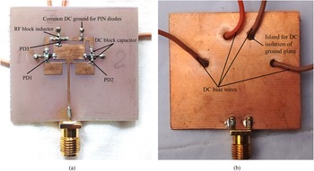
The fabricated FRPA shown in Fig. 3, is characterized for reflection coefficient (S11) and radiation pattern, using Agilent N5222 vector network analyzer (VNA) and Anechoic chamber respectively. The calibration of the VNA is done using thru – reflect – line (TRL) technique. Three RF PIN diode switches mounted at inimitable positions of the asymmetric armed U-slot and reversed L-shaped slots offer eight possible reconfigurable modes relying upon the ON and OFF condition of each PIN diode. However, out of these eight modes of operation, only six modes are considered, as for the other two modes, the measured S 11 is less than −10 dB. The resonant frequency, −10 dB % bandwidth, reflection coefficient and application band covered by different reconfigurable modes of the designed FRPA are given in Table 1.
(a) Front view, (b) Back view of the fabricated FRPA.

Resonant frequency, bandwidth, reflection coefficient S11 and application bands covered for different operating modes.

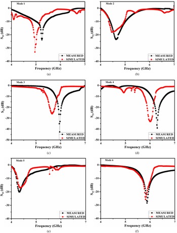
The six modes cover two continuous frequency band ranging from 4.21 to 5.43 GHz (Aeronautical radio navigation, N79 5G, WLAN) and 5.69 to 6.60 GHz (WLAN, Wi-Fi 6E). It is found that, mode 2 provides the highest −10 dB % bandwidth of 13.17% (4.40–5.01 GHz). Measured reflection coefficients S11 of all the six modes are compared with their simulated counterparts and is shown in Fig. 4(a), (b), (c), (d), (e) and (f) respectively.
Simulated and Measured S 11 of the investigated FRPA for its reconfigurable modes.

From these figures, it is seen that the measured results are in good agreement with the simulation data. On average, 0.185 GHz of resonant frequency variation is observed in measured results with respect to simulated values, which can be due to the presence of DC bias wires, actual RF components and solder bumps in the fabricated antenna.
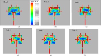
The proposed FRPA reconfigures its resonant frequency on the basis of redistribution of surface current density due to alteration of effective electrical length of the patch upon RF PIN diodes switching. For OFF state of PIN diode switches, the current path elongates as there is no electrical connection across the slot. When a PIN diode mounted over the slot structure is turned ON, it sets a conductive pathway across the slot, lowering the effective path length of the current along with a change in surface current distribution across the slot edge. The resonant frequency of an antenna is inversely proportional to the effective electrical length of the patch [Reference Balanis37]. Therefore, the resonant frequency of the proposed FRPA changes for different switching combinations of the three PIN diodes incorporated with the asymmetric armed U-slot and reversed L-shaped slots. To validate this explanation, simulated surface current densities (J surf) over the patch for six reconfigurable modes are shown in Fig. 5(a), (b), (c), (d), (e) and (f). In mode 1, all PIN diodes PD1, PD2 and PD3 are turned OFF and small current flows through them as depicted in Fig. 5(a). It is seen that, the current mainly flows through the outer periphery of the rectangular slots via DC block capacitors. For mode 2, RF current mainly passes through PD1 as it is turned ON and redistribution of surface current occurs as shown in Fig. 5(b). Similarly, from Fig. 5(c) it is seen that, PD2 mainly conducts current across the slot for mode 3 operation. In mode 4 operation (Fig. 5(d)), PD3 provides low resistive path for RF current to alter the surface current density. In mode 5, PD1 conducts more than PD2 as seen from Fig. 5(e) although PD1 and PD2, both allows current to flow through them. Current flows through all the PIN diodes PD1, PD2 and PD3 to redistribute the surface current densities for mode 6 operation (Fig. 5(f)). With a combination of these (asymmetric armed U and reversed L slot) slots along with PIN diode switches, the FRPA covers a widespan application band from WLAN, N79 5G, aeronautical radio navigation to Wi-Fi 6E (details mentioned in Table 1).
Surface current distribution for different modes of operation.

Moreover, from the S11 measurement, it is found that, for mode 5, the FRPA resonates at 4.33 GHz with a patch dimension Lp = 11.59 mm and Wp = 15.49 mm, which is smaller compared to a conventional rectangular patch antenna designed to resonate at 4.33 GHz. Thus, a size decrease of 46.9% is accomplished at 4.33 GHz for the FRPA. Besides, the designed antenna occupies overall smaller size of (35 × 40) mm2 than the reconfigurable antennas reported in [Reference Mansoul and Seddiki23, Reference Chattha, Hanif, Yang, Abbasi and Rana26, Reference Jin, Deng, Yang, Xu and Liao32, Reference Saikia, Dutta and Borah33].
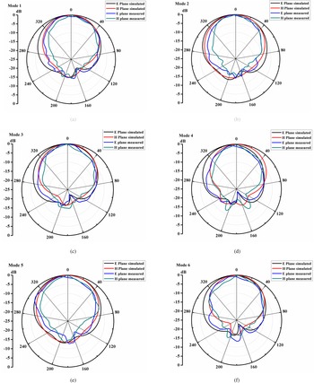
The radiation pattern and gain of the designed FRPA are consistent during the frequency reconfiguration process. To validate the simulated results, an anechoic chamber measurement set-up is employed. The simulated and measured E and H plane radiation patterns of the FRPA are shown in Fig. 6(a), (b), (c), (d), (e) and (f) for all the reconfigurable modes at respective resonant frequencies. From Fig. 6, it can be seen that simulated and measured radiation pattern are almost stable for all of its presented modes. E-plane main lobes are found at 350° while it is 0° for H-plane main lobes for all cases.
E and H-plane radiation pattern of all reconfigurable modes.

The gain of the fabricated antenna is measured using the conventional two antenna method. The simulated gain of the proposed FRPA for mode 1, mode 2, mode 3, mode 4, mode 5, and mode 6 operation is found as 6.58, 6.95, 8.09, 8.17, 6.92, and 7.53 dB respectively while the measured counterparts are 5.86, 6.49, 8.45, 8.72, 6.09, and 8.12 dBi. A comparison plot between the simulated and measured gain of the investigated FRPA for six reconfigurable modes is shown in Fig. 7. As, slot loading is a useful technique for gain enhancement of microstrip patch antenna [Reference Islam, Shakib and Misran38–Reference Ahmad, Sun, Zhang and Samad42]. Selection of suitable slot size and position leads to reduction of side lobe levels in antenna radiation pattern for improvement of directivity and gain of an antenna, which has resulted, a peak gain of 8.72 dBi and average gain of 7.29 dBi for the proposed design geometry. Moreover, return loss S 11 < −20 dB also contributes to high gain, as it indicates the transfer of maximum power to the antenna leading to maximum radiation and hence increment in gain.
Simulated and measured gain at different reconfigurable modes.

In terms of design, performance parameters and applications, a comparison between the proposed FRPA and recently reported relevant works is done, which is presented in Table 2.
Comparison of the designed FRPA with other relevant works (λ 0 is the free space wavelength at the lowest resonant frequency).

Conclusion
A FRPA with three RF PIN diodes mounted on inimitable positions of an asymmetric armed U-slot and a reversed L-shaped slot for aeronautical radio navigation, sub-6-GHz 5G, WLAN, and Wi-Fi 6E applications is reported in this article. Frequency reconfiguration for different PIN diode combinations is obtained at 4.33, 4.63, 5.24, 5.87, 5.96, and 6.29 GHz, covering a continuous frequency band (in terms of −10 dB bandwidth) ranging from 4.21 to 5.43 GHz and 5.69 to 6.6 GHz. Compact dimension, integrated DC biasing circuitry, stable E and H plane radiation pattern, the high average measured gain of 7.29 dBi and a 2.13 GHz of the continuous reconfigurable frequency range are the notable features of the proposed design.
Conflict of interest
The authors declare that they have no known competing financial interests or personal relationships that could have appeared to influence the work reported in this paper.
 Bhaben Saikia obtained M.Sc. in electronics & communication technology from Gauhati University, Assam, India, in 2011. Currently, he is pursuing Ph.D. at the Department of Physics, NERIST, Arunachal Pradesh, India. His research interest includes the reconfigurable antenna, embedded system and mechatronic system.
 Kunal Borah (Corresponding Author) obtained B.Sc. degree in Physics and the M.Sc. degree in Physics with a specialization in electronics and photonics. He has been awarded Ph.D. degree in physics for the study of magnetodielectric substrates for microstrip patch antennas from Tezpur University, India in 2014. He has been awarded Rajiv Gandhi National Fellowship by UGC for carrying out his Ph.D. research in 2007. He is now working as an assistant professor in the Department of Physics, NERIST, Arunachal Pradesh, India. He has authored several papers in international journals, national journals and conference proceedings. His research interest includes magnetodielectric materials, nano electromagnetism, and miniaturized antennas.