Ferrites, double oxides of iron and another metal, represent an important group of ferrimagnets from a technological point of view. With high electrical resistivity and low eddy current losses they are attractive for high-frequency applications where power losses must be minimized.[Reference Cullity and Graham1, Reference Spaldin2]
Nickel ferrite (NFO) is a soft ferrimagnet with an inverse spinel cubic structure with the nickel Ni2+ ions on octahedral sites and the Fe3+ ions evenly divided between octahedral and tetrahedral sites.[Reference Cullity and Graham1] Owing to its wide band gap, high Curie temperature, relatively high saturation magnetization and moderate magnetostrictive effect,[Reference Cullity and Graham1–Reference Srivastava, Ojha, Chaubey and Materny4] NFO is an interesting material for a number of applications, including sensors,[Reference Zhao, Zhao, Hunter, Suchoski, Gao, Mathews, Wuttig and Takeuchi5, Reference Lin, Li, Soh and Li6] microwave[Reference Adam, Krishnaswamy, Talisa and Yoo7] and spin filter devices,[Reference Luders, Barthelemy, Bibes, Bouzehouane, Fusil, Jacquet, Contour, Bobo, Fontcuberta and Fert8, Reference Chapline and Wang9] memory[Reference Chou10, Reference Ross, Haratani, Castano, Hao, Hwang, Shima, Cheng, Vogeli, Farhoud, Walsh and Smith11], and magnetoelectric composites.[Reference Priya, Islam, Dong and Viehland12, Reference Fiebig13] Most of these applications require a high degree of grain orientation (texture) along the NFO <111> easy axis direction. With increasing texture the magnetocrystalline anisotropy increases, reducing the field required to reach the saturation magnetization and improving the magnetostrictive properties. Approaches to synthesize textured NFO thin films include pulsed laser deposition,[Reference Dixit, Singh, Srivastava, Agrawal, Choudhary and Gupta14–Reference Chinnasamy, Yoon, Yang, Baraskar, Vittoria and Harris17] sputtering[Reference Rigato, Estrade, Arbiol, Peiro, Luders, Marti, Sanchez and Fontcuberta18, Reference Venzke, vanDover, Phillips, Gyory, Siegrist, Chen, Werder, Fleming, Felder, Coleman and Opila19], and e-beam reactive evaporation.[Reference Lind, Berry, Chern, Mathias and Testardi20] These methods are costly, time consuming and often give only weakly textured films.
In contrast, a chemical solution deposition (sol–gel) method has been reported to give biaxial texture at fraction of the cost.[Reference Seifikar, Calandro, Deeb, Sachet, Yang, Maria, Bassiri-Gharb and Schwartz21] Additional advantage of the sol–gel method lies in its compatibility with various soft lithography techniques.[Reference Xia and Whitesides22] Among these, nanoimprinting lithography (NIL) provides a low-cost, high-throughput method for nanostructure fabrication in a precise, repeatable, and scalable way.[Reference Guo23–Reference Dinachali, Saifullah, Ganesan, Thian and He26] Despite the numerous advantages of combining NIL with sol–gel deposition, the field of NIL has focused mostly on semiconductor[Reference Chapline and Wang9] and photonic applications;[Reference Wu, Yu, Wang, Williams, Liu, Sun, Zhang, Kim, Shen and Fang27, Reference Dai, Wang, Zhang, Han, Shi, Wang and Du28] minimal work has been reported on the patterning of magnetic materials via NIL. The few examples have reported fabrication of quantum dot arrays for high-density magnetic recording with varying success.[Reference Chou10, Reference Hu, Wilson, Xu, Han and Wang29] In these examples, the manufacturing process is more complex than the approach reported here. Standard NIL procedure includes pressing a patterned stamp onto a photoresist covering the film and then using reactive ion etching (RIE) to create features. This method introduces some constraints on the patterning and requires additional steps to ensure good feature transfer. Here, a modified approach to NIL patterning by directly imprinting the stamp on the thin film before crystallization is reported. Resulting imprints show good pattern transfer with features that are copied with a high degree of precision. Furthermore, the crystallographic texture is not affected by the nanoimprinting process. This constitutes a significant improvement over previously reported work.[Reference Gobel, Nedelcu and Steiner24, Reference Dai, Wang, Zhang, Han, Shi, Wang and Du28]
NFO solution was prepared by mixing iron(III) nitrate non-ahydrate [Fe(NO3)3·9H2O] and nickel(II) acetate tetrahydrate (C4H6NiO4·4H2O) in 2-methoxyethanol (CH3OCH2CH2OH) solvent (all from Sigma-Aldrich) under inert atmosphere. The solution was stirred at 80 °C for 40 min and allowed to cool to room temperature.
For comparison, and evaluation of the procedure, two sample configurations, plain and patterned, were used. For the plain samples, 0.2 M NFO solution was spin coated at 5000 rpm for 30 s onto c-plane (0001) sapphire substrates. Samples were then pyrolyzed at 400 °C for 60 s to remove the solvent. Additional furnace annealing at 750 °C for 600 s was used to fully crystallize the film. The previous work revealed these to be the optimal processing parameters.[Reference Seifikar, Calandro, Rasic, Deeb, Yang, Bassiri-Gharb and Schwartz30]
For the pattern master, a commercially available CD was selected due to its consistent periodic features over large scale, which allow for easy evaluation of the pattern transfer quality. To access the features, the top aluminum layer of the CD was removed and the CD was cleaned using isopropyl alcohol.
A polydimethylsiloxane (PDMS) stamp was prepared using a Sylgard-184 Silicone Elastomer Kit (Dow Corning) by mixing together silicone base and a curing agent in a 10:1 weight ratio. After mixing, the PDMS was poured over the CD master, degased to remove the bubbles and allowed to cure at 80 °C for 24 h, similar to procedures found in the literature.[Reference Efimenko, Wallace and Genzer31] After curing, the PDMS stamp was removed from the master and cut into smaller pieces for patterning.
Next, the PDMS stamp was pressed onto the spin coated NFO thin film with immediate pyrolysis at 400 °C for 60 s. After pyrolysis, the stamp was removed and the patterned film placed in the furnace to crystalize the NFO according to the aforementioned procedure. Samples made with the intermediate patterning step were designated “patterned.”
Surface morphology of the patterned NFO thin films was evaluated using a Cypher atomic force microscope (AFM) by Asylum Research in tapping mode (Fig. 1). An AFM scan of the CD master shows consistent features with a periodicity of ~1.5 µm [Fig. 1(a)]. The features were copied with a high degree of precision to the PDMS stamp [Fig. 1(b)] and to the NFO thin films [Figs. 1(c) and 1(d)]. After demolding, the PDMS stamp had closely mimicked the features of the CD master [Fig. 1(b)]. There were no noticeable deviations from the master pattern, such as uneven, collapsed or broken features, nor were there any gas bubbles present in the PDMS stamp. Good conformity between the CD master and the PDMS stamp resulted in good patterning of the entire PDMS stamp.
AFM images of (a) CD master, (b) PDMS stamp and (c, d) patterned NiFe2O4 thin films grown on (0001) sapphire substrates.

AFM scans of a patterned NFO thin film in two different magnifications are shown in Figs. 1(c) and 1(d). The lower magnification image shows that the pattern transferred over large areas without cracking, bending, misalignment, feature collapse, air gaps or other defects, which are commonly encountered with NIL techniques.[Reference Bietsch and Michel32] At higher magnification, the high level of precision of the pattern and the individual grains making up the nanostructures are observed. Surface morphologies and pattern transfer are easily compared by looking at the roughness analyses also seen in Fig. 1. Feature height in the image from the CD [Fig. 1(a)] appears smaller than in the image from the PDMS [Fig. 1(b)]; this is due to the insufficient aspect ratio of the AFM tip. In the PDMS, the tip is able to probe deeper due to the elasticity of the PDMS stamp. The feature height reduction observed in the NFO thin film [Figs. 1(c) and 1(d)] is due to the limited amount of material due to the NFO thin film thickness after spin coating. Further analysis of Fig. 1(d) shows that the features in the patterned sample are made up of individual grains, indicating that there was no growth disruption of the NFO thin film by the PDMS stamp during the patterning process.
Transmission electron microscopy (TEM) images of the sample cross-sections were taken using a JEOL 2010F TEM. TEM sample preparation used focused ion beam (FIB) milling on a FEI Quanta three-dimensional (3D) FEG microscope. Before ion milling, samples were carbon coated to prevent charging.
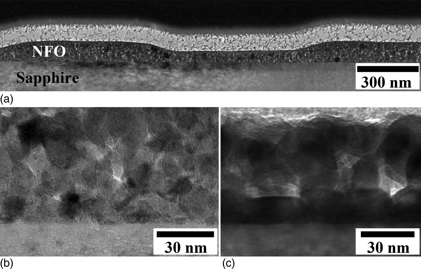
Cross-sectional TEM images of a patterned NFO thin film (Fig. 2) show that the film is 55 nm thick with 45 nm feature height and 1.5 µm periodicity. Surface features are sharp and precise with no apparent growth disruption by the PDMS mold. These results are consistent with the AFM results. No nucleation sites form at the NFO/PDMS interface during the patterning process, which is attributed to the insufficient thermal budget at the PDMS stamp/NFO interface during patterning.
TEM cross-sectional images of (a, b) patterned and (c) plain NiFe2O4 thin film grown on a (0001) sapphire substrate.
An image of the plain sample [Fig. 2(c)] shows individual grains growing from the substrate indicating that the nucleation proceeds via an island growth (Volmer-Webber) mechanism.[Reference Nalwa33] Low lattice mismatch and favorable substrate orientation with the c-plane (0001) sapphire substrate cause the NFO thin film to crystalize preferentially in the easy axis (111) direction.[Reference Seifikar, Calandro, Deeb, Sachet, Yang, Maria, Bassiri-Gharb and Schwartz21, Reference Seifikar, Calandro, Rasic, Deeb, Yang, Bassiri-Gharb and Schwartz30] If the thermal budget is optimum, nucleation from the substrate will fully crystallize the film before surface nucleation begins.[Reference Schwartz34] Comparing different samples [Figs. 2(b) and 2(c)], less grain orientation is observed and there is no evidence of substrate nucleation in the patterned sample [Fig. 2(b)], indicating the need for different processing conditions, i.e. an optimized thermal budget, for the patterned thin films.
X-ray diffraction (XRD) was used to compare the crystal structure and chemical composition of plain and patterned films. XRD θ–2θ scans were performed from 15° to 60° using Cu Kα radiation (λ = 1.5418 Å) in a Smartlab Rigaku X-Ray diffractometer. XRD data for both configurations show the NFO inverse spinel structure with no impurity phases (Fig. 3). The peaks were calculated using Bragg's law and correlated with the reference PDF file.[35] In both cases, only peaks corresponding to the <111> family of planes are observed, confirming that the films are somewhat textured. This is in accordance with similar work on biaxially textured NFO thin films[Reference Seifikar, Calandro, Deeb, Sachet, Yang, Maria, Bassiri-Gharb and Schwartz21] and consistent with other reports on epitaxial grown NFO thin films.[Reference Chinnasamy, Yoon, Yang, Baraskar, Vittoria and Harris17, Reference Venzke, vanDover, Phillips, Gyory, Siegrist, Chen, Werder, Fleming, Felder, Coleman and Opila19] Comparing the peaks present and their intensity (Fig. 3), the texture in the patterned and plain films are the same; there is no noticeable grain misorientation or new phase formation in the patterned film. This confirms that there was no significant grain growth disruption by the PDMS stamp during the patterning process nor were there new nucleation sites formed at the NFO/PDMS interface.
XRD patterns of (a) plain and (b) patterned NiFe2O4 thin films.
Magnetic properties were measured at room temperature using a Quantum Design superconducting quantum interference device (SQUID) with the magnetic field parallel to the thin film surface and magnetic field up to ±7 T. The substrate contribution to the measured magnetic data was removed and the data were normalized to the NFO thin film volume; the resulting magnetic hysteresis curves for the plain and patterned samples are shown in Fig. 4. For comparison, magnetic data for an area of film that was not patterned are also shown.
Magnetization hysteresis measurements of plain, patterned and non-patterned NiFe2O4 thin films. The inset shows the significant reduction in coercivity in the patterned film.
Saturation magnetization (M s) values of plain and non-patterned samples are similar, 120 and 118 emu/cm3, respectively, and somewhat smaller than the results reported elsewhere.[Reference Seifikar, Calandro, Deeb, Sachet, Yang, Maria, Bassiri-Gharb and Schwartz21] This reduction is attributed to using a lower molarity solution, 0.2 M, compared to 0.5 M reported previously. The saturation magnetization of the patterned sample is reduced to 67.5 emu/cm3, a ~44% reduction as compared to the plain samples. As the AFM, TEM, and XRD measurements show no evidence of reduced crystallinity or damage in the patterned film, this is attributed to a larger surface to volume ratio. This in turn results in larger porosity and reduced long-range magnetic order in the patterned film.[Reference Heh and Chen36]
Coercivity differences are seen in the magnetic hysteresis curves shown in the inset of Fig. 4. Comparing the coercivity (H c) of plain and non-patterned samples, they again have similar values, 230 and 210 Oe, respectively. The patterned sample, however, shows a significantly smaller value of 25 Oe, a reduction of ~89%. Typically one expects an increase in coercivity with higher surface roughness due to changes in domain wall movement.[Reference Zhao, Gamache, Wang, Lu, Palasantzas and Hosson37, Reference Jiang, Yang and Wang38] Instead the opposite is observed. Here, the dominant factor is not the domain wall movement but the in-plane demagnetization factors that are amplified by the anisotropy of surface morphology.[Reference Zhao, Palasantzas, Wang and De Hosson39–Reference Ding, Thibado, Awo-Affouda and LaBella41] The demagnetizing field reduces the coercivity by close to 90% of the initial value. This result may be of significant technological importance, as the approach may facilitate tuning of the coercivity.
In summary, textured NFO films were deposited on c-plane sapphire substrates via sol–gel deposition. Patterned NFO thin films were prepared using a modified NIL technique. The pattern from the master was transferred completely and with high degree of precision over large areas without affecting the nucleation, grain growth or texturing due to insufficient thermal budget at the PDMS interface. Thus, the films remained textured in patterned films while simultaneously modifying the surface. Magnetic measurements show large reduction in coercivity with patterned thin films due to the demagnetization field. Thus, the coercivity of films may be tuned by surface modification at the nanoscale, making them particularly interesting in high-frequency applications where further reduction in the power losses can be obtained. The limit to patterning size depends on many factors. Based on the grain size one can estimate the lower limit to at least a few hundred nanometers. The relationship between pattern size and magnetic properties remains to be explored. The reported patterning method represents a fast, inexpensive, easy, versatile, and scalable method for large-scale surface design of sol–gel derived textured thin films.
Acknowledgements
The authors would like to thank Dr. Nazanin Bassiri-Gharb and Elisabeth Deeb for supplying the NFO solution and Dr. Jan Genzer and Dr. Kirill Efimenko for their help with the PDMS stamp. The authors acknowledge the use of the Analytical Instrumentation Facility (AIF) at North Carolina State University, which is supported by the State of North Carolina and the National Science Foundation. Authors would also like to thank Dr. Yi Liu for his help with FIB and TEM measurements.