Anodization of aluminum for the protection and decoration of the metal surfaces has been widely used in industry since the beginning of the 20th century. The first patent on the porous anodic alumina was filed in 1898.[Reference Pollak1] Various theories[Reference O'Sullivan and Wood2, Reference Diggle, Downie and Goulding3] attempted to explain the formation of porous structure and effort in this direction still continues.[Reference Hebert, Albu, Paramasivam and Schmuki4, Reference Sulka and Eftekhari5] In 1995, ordered anodic aluminum oxide (AAO) discovered by H. Masuda and K. Fukuda attracted the attention of the research community, owing to the possibility of obtaining self-organized porous films using two-step replication anodization.[Reference Masuda and Fukuda6] This discovery led to a break-through in the synthesis of ordered structures with a very narrow pore size distribution.
AAO membranes, owing to their straight pores with a controllable diameter, length and inter-pore distance, are widely used for template synthesis of nanowires,[Reference Lu, Chang and Fan7–Reference Wu, Lin and Shau9] nanorods[Reference Lukatskaya, Trusov, Eliseev, Lukashin, Jansen, Kazin and Napolskii10, Reference Matsui, Kyotani and Tomita11] and nanotubes[Reference Lee, Scholz, Nielsch and Gösele12–Reference Kyotani, Tsai and Tomita14] with a customizable diameter and geometry[Reference Shingubara15]. Applications of 1D nanostructures have been reviewed in Refs.Reference Farrell, Petkov, Morris and Holmes16–Reference Xia, Yang, Sun, Wu, Mayers, Gates, Yin, Kim and Yan18. A number of articles have been published detailing the synthesis of porous films with either an ultra-small[Reference Ding, Yang, Ding, Yuan and Zhu19] channel diameter or submicrometer pores, along with advanced nanochannel designs such as branches or periodical oscillations.[Reference Lee, Ji, Gosele and Nielsch20–Reference Nagaura, Takeuchi and Inoue24] However, the architecture of porous AAO has so far been limited to the flat porous films. In this paper, we report the observation of complex three-dimensional (3D) structures from porous anodic alumina and suggest a mechanism for their formation.
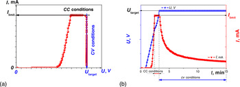
Aluminum foils (99.99%, 0.25 mm-thick, annealed, Alfa Aesar, Ward Hill, Massachusetts, USA) of 1 cm2 area were used as a starting material. Prior to anodization, foils were treated by 1 M NaOH solution for 15 min in order to remove a thin oxide layer from the surface. Anodization of aluminum was carried out for 1–3 h in a two-electrode cell in 250 mL of 0.3 M (COOH)2 + 3 M C2H5OH solution using a graphite rod as a counter electrode. Voltage was gradually increased at a rate of 1 V/s to the target voltage (U target) that varied from 100 to 150 V, while the current limitation (I limit) on the power supply was set at 250–400 mA. Therefore, as shown in Figs. 1(a) and 1(b), while increasing the voltage, the current value also increased to the I limit value and remained constant (constant current conditions = CC) until the voltage reached U target (constant voltage conditions = CV), upon which the current decreased. The electrolyte temperature was kept at −1 °C. To separate the porous oxide film from aluminum, the latter was dissolved in a solution of 7.56 g of CuCl2 in 200 mL deionized water and 200 mL of concentrated HCl at room temperature. Subsequently, the dissolution of the barrier layer and widening of pores was carried out in a 5 vol% H3PO4 aqueous solution at 60 °C. Scanning electron microscopy (SEM) analysis was performed on Zeiss Supra 50 VP (Carl Zeiss SMT AG, Oberkochen, Germany).
Aluminum anodization conditions: (a) C–V curve schematic with vertical and horizontal plateaus representing constant current and constant voltage regimes, (b) typical time dependences of the current and voltage variations during anodization.

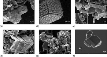
The high-magnification SEM images of complex nanostructures formed from porous anodic alumina are presented in Figs. 2 and 3. Most of the hollow tetragonal and cubic structures are assembled into hierarchical arrays. Formation of such structures takes place from a side of the barrier layer at the metal/oxide interface. Therefore, one is able to observe them only after complete or partial dissolution of the aluminum (as they are covered by it). The images in Figs. 2(a)–2(e) were taken after barrier layer removal in H3PO4, though the inset in Fig. 2(c) illustrates a fragment of the as-produced nanostructure. In Fig. 2(e), image of porous oxide framework with incomplete removal of aluminum is presented. In Fig. 2(f), tetragonal AAO nanostructure can be seen under the aluminum. It is worth noting that the observed structures possess a continuous open surface (cracks visible in some images are due to sample preparation).
SEM images of the tetragonal and cubic structures from porous anodic alumina: (a)–(d) after barrier layer etching, the inset in (c) illustrates the fragment of such structures prior to the barrier layer removal; (e) and (f) after partial Al dissolution.

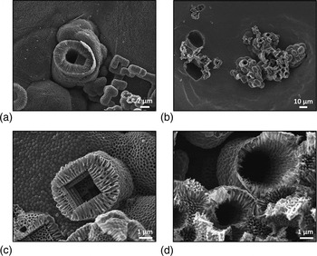
3D nanostructures from porous AAO.

The growth of these structures is associated with a local electrical breakdown that usually takes place when anodization is performed at high voltages and high current densities (hard anodization technique). The breakdown originates from a voltage increase at rates that do not allow for the electric field to uniformly distribute itself throughout the region, which leads to a localized electrochemical breakdown and subsequent Joule heating. The localized nature of the nucleation of complex structures was confirmed by microscopic observations (Fig. 3).
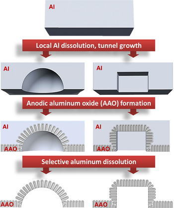
Considering the formation of pores in an AAO film takes place perpendicular to the Al surface, the oxide film microstructure follows the morphology of the metal surface. Therefore, the formation of the 3D architecture of the anodic alumina is contingent on a modification of the Al surface before the oxide growth. A possible explanation of such observation is that Al foil is locally etched during local break down. This effect is similar to the formation of pits in aluminum foils, which takes place at galvanostatic conditions and current densities at 200–300 mA/cm2.[Reference Osawa and Fukuoka25] For our experiment, galvanostatic conditions were maintained with comparable values of current densities until the voltage reached its target value. Most likely, formation of the tunnels in the Al is driven by the mechanism of Al pitting described in,[Reference Lee, Kim and Gosele23, Reference Osawa and Fukuoka25] also in constant current regime. The schematic representation of the possible mechanism of 3D complex nanostructure formation from porous anodic alumina is shown in Fig. 4.
Tetragonal and hemispherical structure formation from porous anodic alumina. The sequence is the following: (1) formation of a thin oxide film during voltage rise, (2) local electrical breakdown of the formed oxide layer, (3) pitting of the aluminum, (4) healing of the breakdown and formation of the AAO layer replicating the pit shape. The oxide can be released by dissolving the aluminum substrate.

During the first stage, local dissolution of the Al takes place during the local electrical breakdown. Depending on the breakdown conditions (local current density and the duration of the process) two types of the tunnels are formed: hemispherical and tetragonal. The former can be observed at higher current densities and for shorter break-down times[Reference Osawa and Fukuoka25] when metal dissolution takes place without regarding the lattice structure, while formation of the tetragonal tunnels with a well-developed structure occurs according to Al crystallography and pits have a tetragonal shape.
During the second stage, when breakdown is healed by the formation of a sufficiently thick alumina layer, the conventional anodization regime is activated. Replication of the tunnel morphology by the porous oxide layer is observed. Interestingly, the thickness of the oxide for these structures is less than 200 nm (Fig. 2). As the length of the tunnels can be on the scale of tens of microns, the diffusion of the oxygen-containing ions to the Al/AlOx interface may be significantly impeded, leading to a much lower oxide growth rate. Finally, Al dissolution and etching of the barrier layer reveal the porous oxide replica of the tunnels in the Al foil.
Therefore, the use of selective dissolution process produces a 3D architecture on the Al surface and offers a possibility to create various complex structures from porous anodic alumina.
Acknowledgments
The authors are grateful to Boris Dyatkin for valuable comments on the manuscript. SEM analysis was carried out using instruments of the Centralized Research Facility (CRF) of the College of Engineering, Drexel University. This work was supported by the NSF NIRT project CBET-0609062.