I. INTRODUCTION
Standard conventional wireless data acquisition systems (e.g. Bluetooth or ZigBee) do not meet medical standards because their size and power consumption specs leave them vulnerable to external signal interference, thus compromising signal quality and safety. In addition, given that a single patient may be simultaneously connected to a large number of sensors, such a system would be excessively bulky. Based on these concerns, the US Federal Communications Commission and its counterparts in other countries have allocated a specific frequency band (402–405 MHz) for medical implant communication systems (MICS) of sensor network.
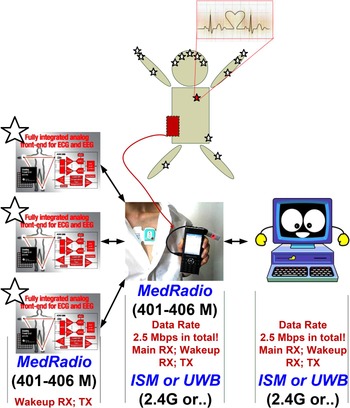
The MICS frequency band spans 402–405 MHz, with an overall bandwidth of 3 MHz, and a channel bandwidth of 300 KHz, allowing wireless communication between medical devices, thus providing increased comfort, mobility, and quality of patient care services [Reference Yuce, Ng, Myo, Lee, Khan and Liu1–Reference Hsu, Lee, Yo and Luo3]. The 402–405 MHz frequency band is conducive to wireless signal transmission, and the propagation characteristics of the band are such that signals in this range do not constitute a significant physical risk to humans nor are they particularly vulnerable to interference from other signal transmissions. The MICS band is subject to certification standards, and offers advantages including ultra-low power consumption and large data transfer capacity, making it suitable for use in medical diagnostics and patient monitoring, as showing in Fig. 1.
MICS system application of sensor network.

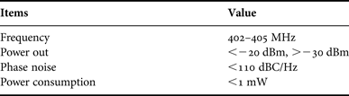
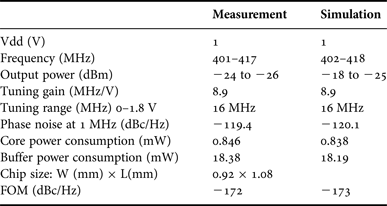
The proposed design references the MICS frequency band in the development of medical application, with particular emphasis on electronic implants. Given the considerable size of the artificial implant systems, we focus here on the design of the wireless transmitter with the aim of using baseband signals to directly modulate out antenna radiation, producing a low-power, voltage-controlled oscillator circuit, with specifications summarized in Table 1.
MICS frequency VCO specifications.

II. OSCILLATOR DESIGN
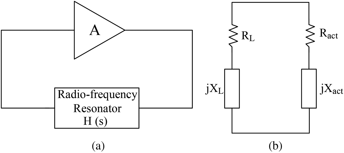
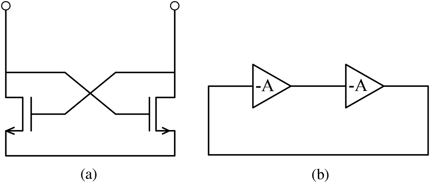
The principles behind the oscillator design are primarily based on Barkausen feedback analysis methods resolved using negative resistance methods. Figure 2(a) illustrates a typical oscillator architecture, including an amplification network with power gain of A and a frequency-selecting resonator with transfer function of H(s). A must be sufficiently large to ensure the stability of the oscillation signal. Simulation analysis indicates that resonator loss is primarily due to the parasitic resistance of inductance exceeding that of capacitance, and the Q value is the imaginary part of impedance divided by the real part of it.
(a) Basic oscillation feedback network. (b) Negative resistance model.

As shown in Figure 2, the oscillator is divided into two parts: the LC resonator and the active component. According to the Barkausen law, oscillation occurs when the real part of the entire circuit impedance is negative and the imaginary part is zero (X L + X act = 0).
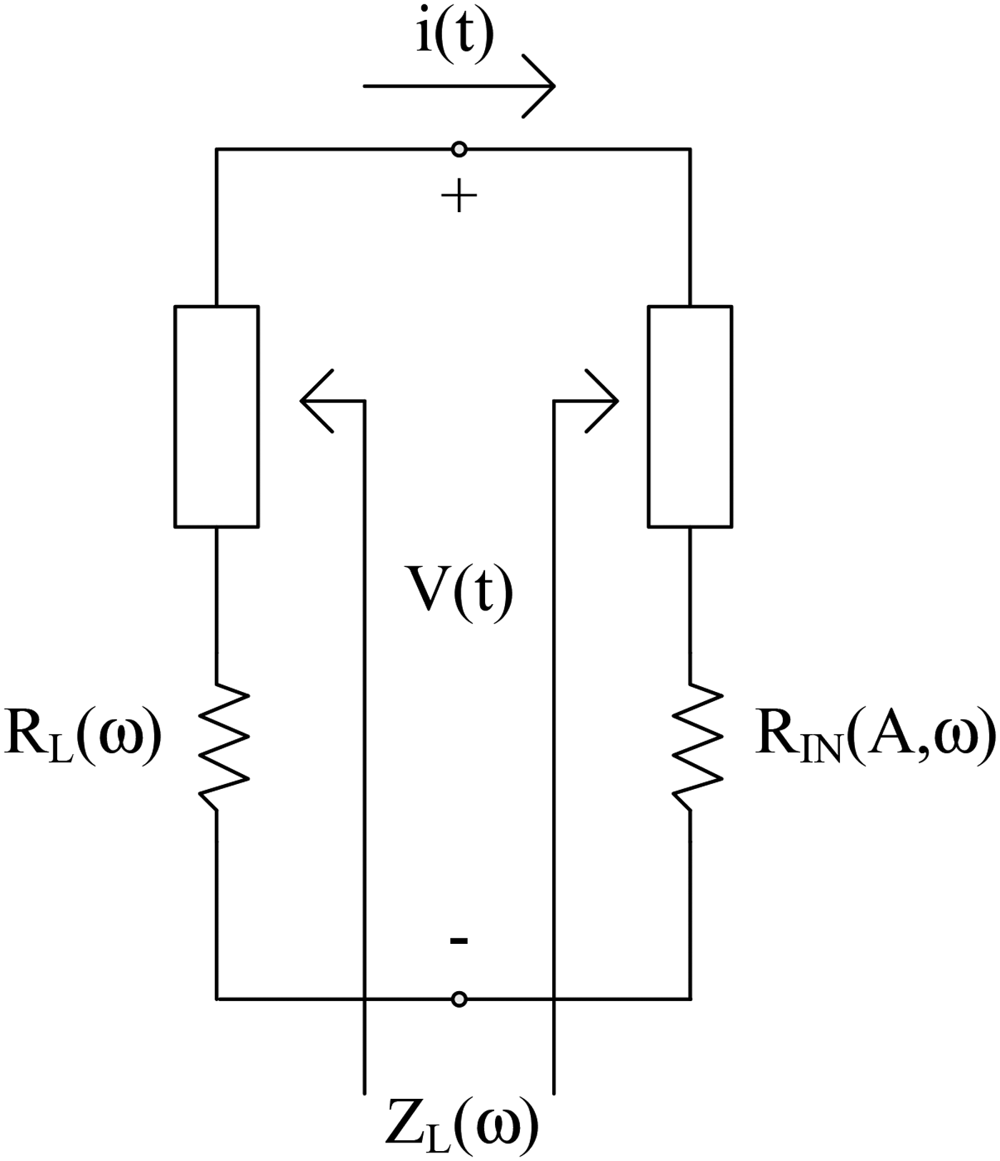
Figure 3 illustrates the single-port oscillator, input impedance of the active device represented by the function of amplitude and frequency can be expressed in equation (1):
 $$Z_{IN} \lpar A\comma \; \omega \rpar =R_{IN} \lpar A\comma \; \omega \rpar +jX_{IN} \lpar A\comma \; \omega \rpar \comma \; $$
where A is the amplitude of the current i(t) and R IN (A, ω) < 0. This element is subject to a passive load impedance:
 $$Z_L \lpar \omega \rpar =R_L \lpar \omega \rpar +jX_L \lpar \omega \rpar .$$
Single-port negative resistance oscillator.

(5)–(9) As oscillation occurs, total impedance approaches to zero:
 $$Z_{IN} \lpar A_0\comma \; \omega _0 \rpar +Z_L \lpar \omega _0 \rpar =0.$$
The real and imaginary parts are separated:
 $$R_{IN} \lpar A_0\comma \; \omega _0 \rpar +R_L \lpar \omega _0 \rpar =0.$$
 $$X_{IN} \lpar A_0\comma \; \omega _0 \rpar +X_L \lpar \omega _0 \rpar =0.$$
When initial oscillation occurs, R IN (A, ω) must exceed R L (ω). This can be written as R IN (0, ω) > R L (ω). As the amplitude gradually increases to A = A 0 and ω = ω 0, the net loop resistance R IN (A, ω) + R L (ω) will approach to zero and achieve a steady-state oscillation. To accommodate these changes, the Z IN (A, ω) must change with the amplitude A and the frequency ω. Since Z IN (A, ω) is impacted by the amplitude and frequency, the frequency determined by equations (4) and (5) will not be stable, thus we must search again for conditions which ensures stable oscillation. Kurokawa proposed additional conditions as follows:
 $$\eqalign{&\left. {\displaystyle{{\partial R_{IN} \lpar A\rpar } \over {\partial A}}} \right\vert _{A=A_0 } \left. {\displaystyle{{\partial X_L \lpar \omega \rpar } \over {d\omega }}} \right\vert _{\omega=\omega _0 } \cr & \quad- \left. {\displaystyle{{\partial X_{IN} \lpar A\rpar } \over {\partial A}}} \right\vert _{A=A_0 } \left. {\displaystyle{{dR_L \lpar \omega \rpar } \over {d\omega }}} \right\vert _{\omega=\omega _0 }\gt 0.} $$
Since dR L ≤ (ω)/dω| ω = ω 0 = 0. Equation (6) can be simplified as follows:
 $$\left. {\displaystyle{{\partial R_{IN} \lpar A\rpar } \over {\partial A}}} \right\vert _{A=A_0 } \left. {\displaystyle{{dX_L \lpar \omega \rpar } \over {d\omega }}} \right\vert _{\omega=\omega _0 }\gt 0.$$
In conclusion, equations (4)–(6) give the conditions for stable oscillation.
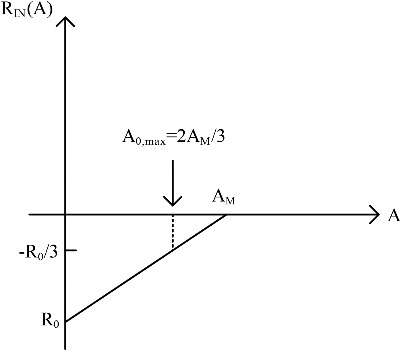
For maximum oscillation power consideration. As shown in Fig. 4, R IN (A) can be expressed as follows:
 $$R_{IN} \lpar A \rpar =- R_0 \left({1 - \displaystyle{A \over {A_M }}} \right)\comma \; $$
Current amplitude varies linearly with negative resistance.

the output power can be written as:
 $$P=\displaystyle{1 \over 2}Re[{VI^\ast }] =\displaystyle{1 \over 2}\vert {I^2 } \vert \vert {R_{IN} \lpar A\rpar } \vert =\displaystyle{1 \over 2}A^2 R_0 \left[{1 - \displaystyle{A \over {A_M }}} \right]\comma \; $$
with a differential extreme value of:
 $$\displaystyle{{dP} \over {dA}}=\displaystyle{1 \over 2}R_0 \left[{2A - \displaystyle{{3A^2 } \over {A_M }}} \right]=0.$$
Thus, we can obtain the maximum current output amplitude A 0,max = 2AM/3, with R IN (A 0,max) = −R 0/3. Because of the stable oscillation, the net loop resistance is zero, thus the R L of maximum power is generated as:
 $$R_L=\displaystyle{{R_0 } \over 3}.$$
In conclusion, design of the negative resistance oscillator is summarized as follows:
-
(1) Select a transistor that is stable at the desired oscillation frequency of ω 0.
-
(2) Design the load impedance using conditions as follows:
(12) $$X_L \lpar \omega _0 \rpar =- X_{IN} \lpar \omega _0 \rpar .$$
(13)
$$R_L=\displaystyle{{R_0 } \over 3}.$$


However, immediately following oscillation, the oscillation power will gradually increase until the transistor's negative resistance is equal to the load resistance. Since X IN is a function of the amplitude A, X IN will also change, thus slightly shifting the oscillation frequency.
III. LOW-POWER VOLTAGE-CONTROLLED OSCILLATOR DESIGN
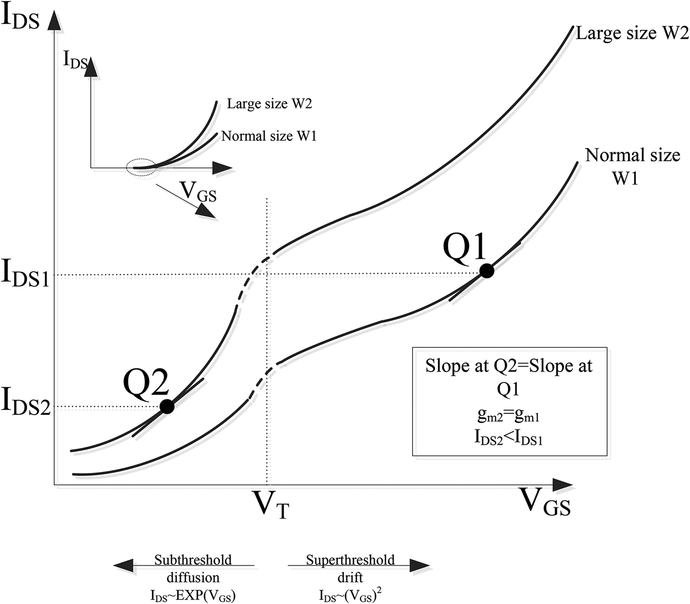
To operate at low power, the transistor must be relatively large because g m is defined as I DS − V GS through the slope of equation (14). Figure 5 shows that a larger size in Q1 and a smaller size in Q2 have the same slope, (same g m ) [Reference Lee and Mohammadi4]. Thus, larger transistor size can obtain the same g m with lower current. Operating the larger transistor in the subthreshold region has a lower I DS where the I DS − V GS relationship is an exponential function (equation (15)). By contrast, the I DS − V GS of W1 is a squared function.
 $$g_m=\left. {\displaystyle{{\partial I_D } \over {\partial V_{GS} }}} \right\vert _{VDS\comma const} .$$
 $$I_D=I_0 \hbox{exp}\displaystyle{{V_{GS} } \over {\xi V_T }}.$$
Comparison of two I DS –V GS curves, in the vicinity of VT, with different sizes.

On the other hand, the exponential I DS –V GS in the subthreshold region can be used to obtain a high gain in an Metal Oxide Semiconductor (MOS) device. Such a scenario would occur for a large transistor width. However, large size would lower operation speed, causing a significant impact on the ring oscillator. Thus, LC tank architecture used in higher frequency voltage-controlled oscillator (VCO) has a higher oscillation frequency, allowing the parasitic capacitance introduced by the larger transistor to reduce the oscillation frequency, as inferred in equation (16).
 $$f_{OSC}=\displaystyle{1 \over {2\pi \sqrt {LC} }}.$$
For the design of VCOs with lower oscillation frequencies, larger transistors can reduce the demand on the LC value. As shown by equation (16), when the f osc is significantly larger, transistor's parasitic capacitance reduces the required LC value, further reducing passive components and chip area, which meets the above-mentioned conditions for the oscillator used in this MICS system.
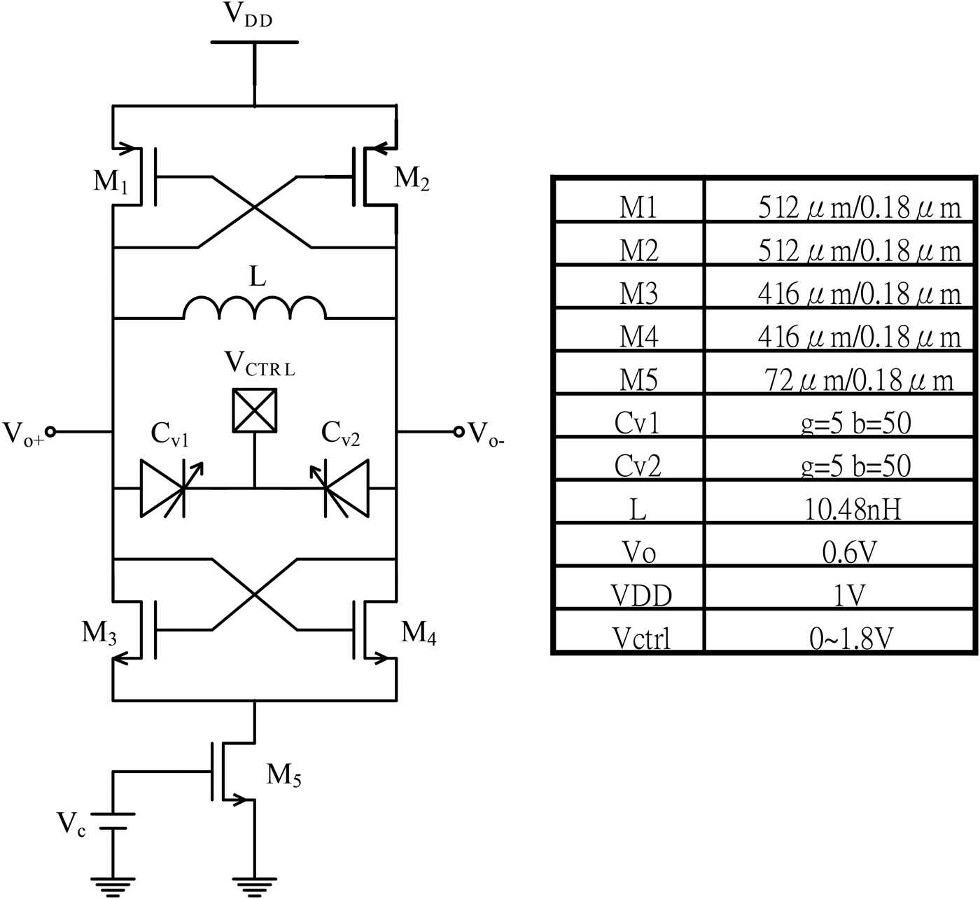
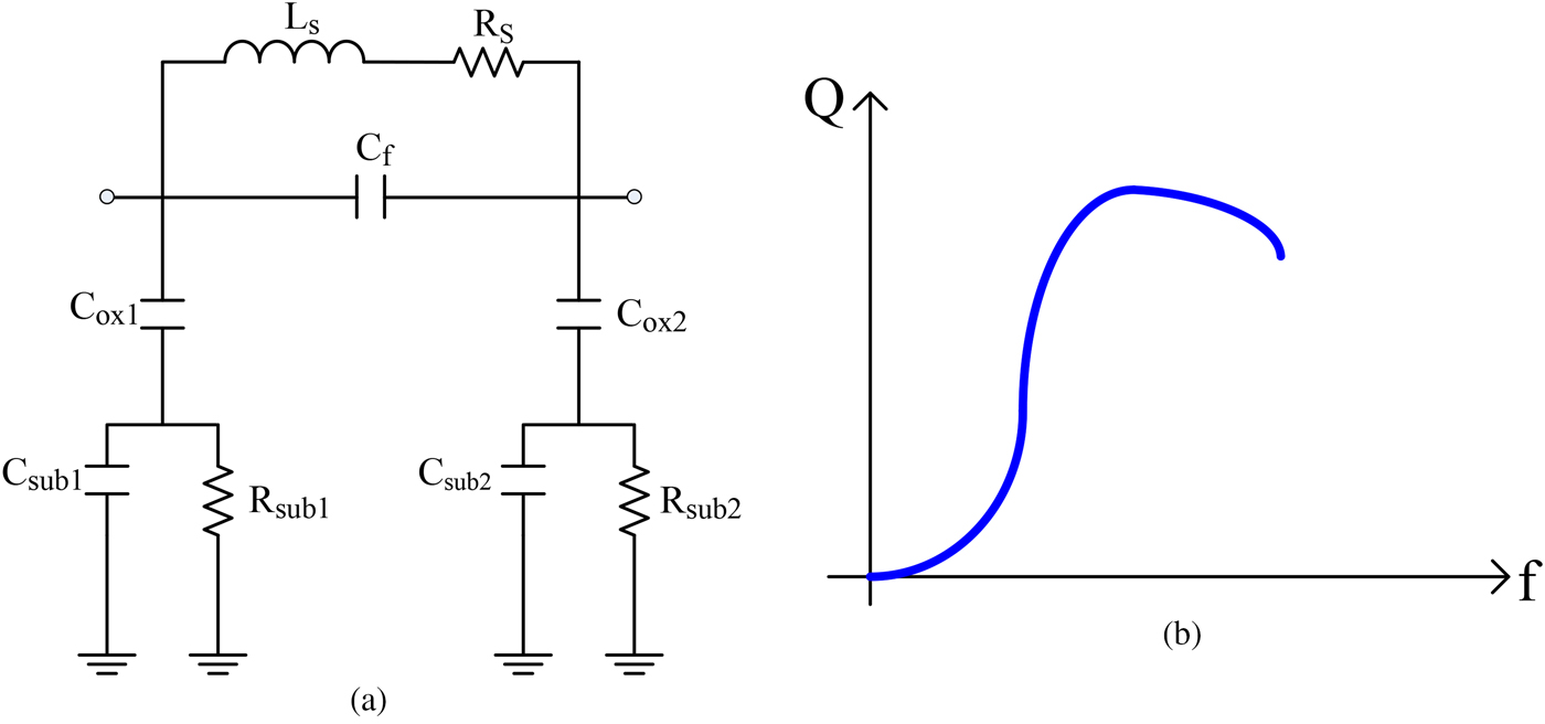
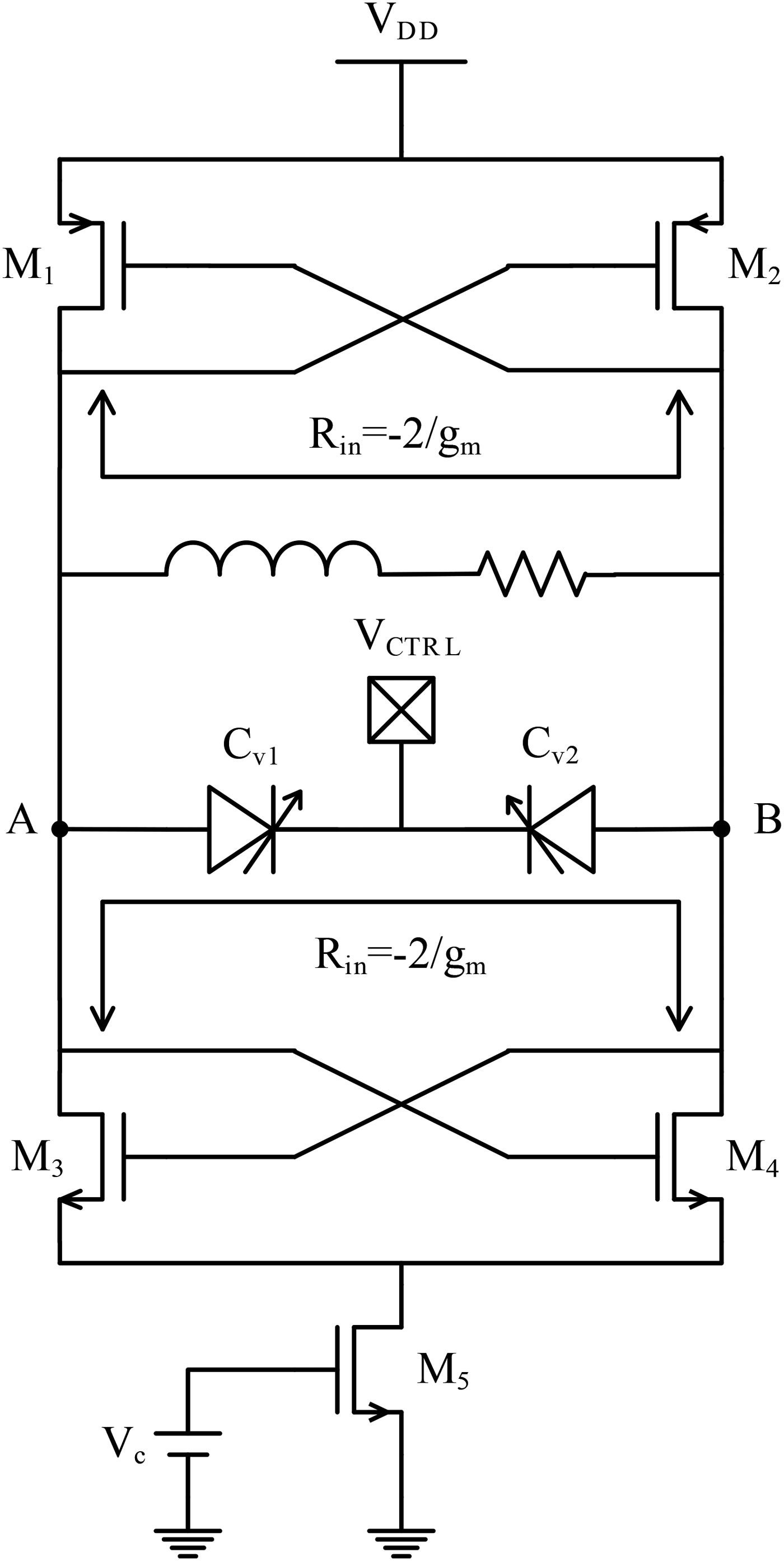
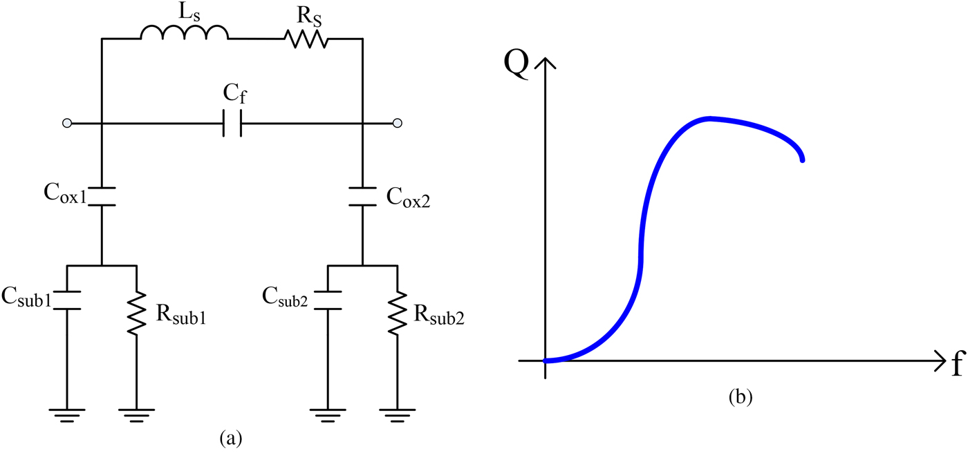
Figure 6 illustrates the proposed circuit structure for the low-power VCO design of the MICS frequency band. The oscillation frequency of the resonator is obtained using equation (16). In general, since Q factor of the capacitance is considerably higher than that of the inductance, energy loss of the LC resonator is primarily dominated by the inductance. The impact of an inductive energy loss can be roughly divided into three parts. The first part is the resistance of the metal at low frequencies, where R s represents the parasitic resistance, R sub represents the substrates equivalent resistance, C f represents the parasitic capacitance, thereby, the inductor's quality factor (Q) can be expressed as:
 $$Q=\displaystyle{{\omega L_s } \over {R_s }}.$$
Low-power VCO design of the MICS frequency band.

Generally speaking, the thicker the upper layer of metal, the better the inductance quality factor (Q). The second part of the inductance energy loss is the capacitive coupling loss. From the inductor equivalent circuit shown in Fig. 7(a), the inductive energy is coupled to the base through a capacitor C ox . Energy loss occurs through the base capacitor C sub and the base resistor R sub , thus the parasitic capacitance between the metal and the base decreases at higher levels.
(a) Inductor equivalent circuit, (b) relationship between inductor quality factor (Q) and frequency.
The third part of the inductor energy loss is magnetically coupled loss, including the well-known skin effect. The metal resistance rises with the operating frequency because the current is no longer uniformly distributed within the metal, but has become concentrated on the metal surface. The depth can be expressed as:
 $$\delta=\displaystyle{1 \over {\sqrt {\pi f\mu \sigma } }}\comma \; $$
where μ represents the magnetic permeability of the metal, σ represents the metal's conductivity, and f represents the operating frequency. Thus, the resistance of the metal's skin effect is expressed as:
 $$R_S=\displaystyle{1 \over {\sigma \delta }}=\sqrt {\displaystyle{{\pi f\mu } \over \sigma }} .$$
The metal's resistance rises with the square root of the frequency. The CMOS process creates a conductive substrate. Thus, when a magnetic field is generated by a spiral inductor current through the substrate, this induced current is referred to as an eddy current because Lenz's law holds that the base current will be induced in the opposite direction. Because the substrate resistance is neither zero nor infinity, therefore some of the energy will be lost. Because the eddy current will cause the resistance of the spiral inductor's inner ring to increase rapidly, thus most of the spiral inductor's inner ring is hollow. The inductor's quality factor increases with the frequency. However, at high operating frequencies, the capacitive and magnetic coupling loss cause the inductor quality factor (Q) to decrease as frequency increases, as shown in Fig. 7(b).
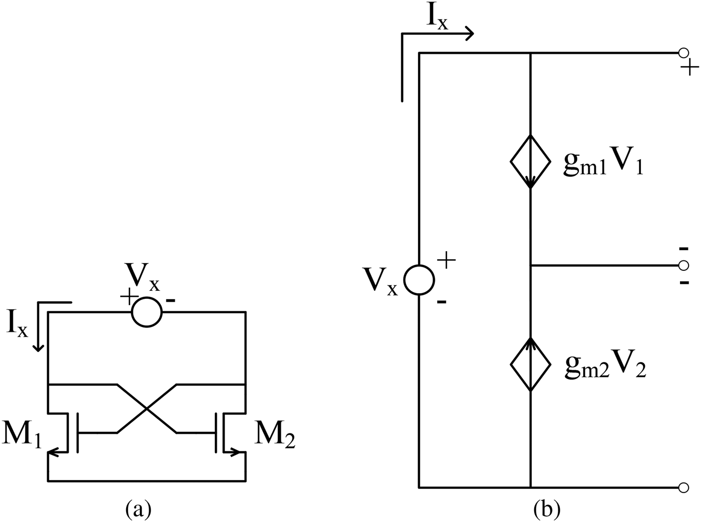
In fact, from the description above, it is impossible to produce a lossless inductor and capacitor. However, the energy provided by the active component satisfies the lossless characteristics and is sufficient to stabilize the oscillation circuit. Figure 8(a) shows the cross-coupled circuit, which can be seen as a closed-loop circuit consisting of two cascading common source circuits. Figure 8(b) shows that these two common source amplifiers form a positive feedback loop, with an overall phase of 360°. Thus, the weak trigger noise produces oscillation, which can be explained by the circuit analysis.
(a) Cross-coupled circuit. (b) Cross-coupled circuit equivalent schematic.

The small-signal equivalent circuit in Fig. 9 shows:
 $$i_x=g_{m1} v_{gs1}=- g_{m2} v_{gs2} .$$
 $$v_x=v_{gs2} - v_{gs1} .$$
(a) Signal analysis of the cross-coupled circuit and (b) small-signal equivalent circuit schematic of (a).

From equation (20) we obtain:
 $$\displaystyle{{v_{gs2} } \over {v_{gs1} }}=- \displaystyle{{g_{m1} } \over {g_{m2} }}.$$
Divide equation (21) by equation (20) to obtain:
 $$\displaystyle{{v_x } \over {i_x }}=\displaystyle{{v_{gs2} - v_{gs1} } \over {g_{m1} v_{gs1} }}.$$
Bring equations (22) into (23) to deduce:
 $$\displaystyle{{v_x } \over {i_x }}=- \left({\displaystyle{1 \over {g_{m1} }}+\displaystyle{1 \over {g_{m2} }}} \right).$$
Assuming that g m = g m 1 = g m 2, then:
 $$\displaystyle{{v_x } \over {i_x }}=\displaystyle{{ - 2} \over {g_m }}.$$
From equation (25), a positive feedback cross-coupled circuit can be a negative resistance equivalent. We know that the resistance is the source of the energy loss, while the negative resistance is the source of the generated energy.
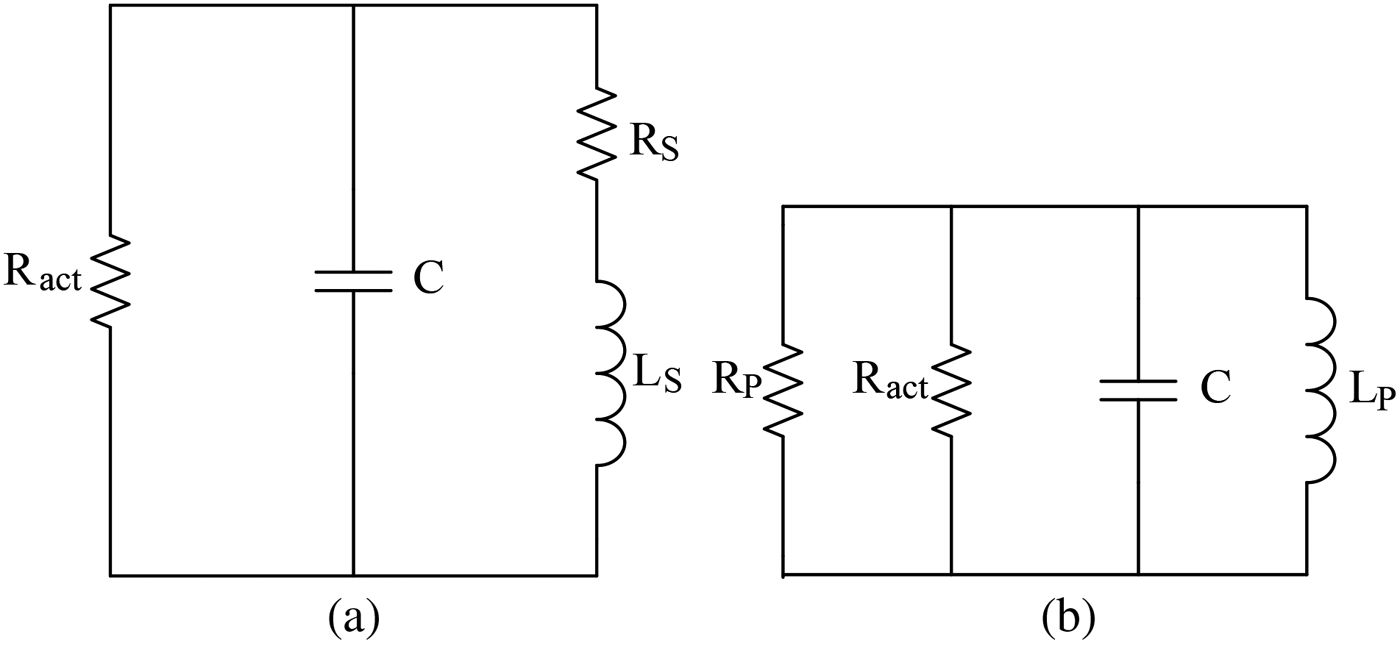
To produce oscillation, the circuit analysis results must have a negative resistance. From Fig. 10 we calculate the equivalent circuit linking the two nodes A and B (parallel connection). This is simplified in Fig. 11(a), where R act represents the equivalent resistance of the two cross-coupled circuits, with a value of −1/g m . C represents the equivalent capacitance found between nodes A and B, while R s represents the inductor's actual parasitic serial resistance, and L s represents the ideal inductance, with the Q value calculated as follows:
 $$Q=\displaystyle{{\omega L_s } \over {R_s }}.$$
Ultra low-power VCO equivalent of the MICS frequency band.

(a) VCO equivalent model and (b) parallel conversion equivalent model for (a).

Operating frequency ω is obtained as follows:
 $$\omega=\displaystyle{1 \over {\sqrt {LC} }}\comma \; $$
via conversion Equations (28) and (29):
 $$R_P=R_S \lpar Q^2+1\rpar .$$
 $$L_P=L_S \left({1+\displaystyle{1 \over {Q^2 }}} \right).$$
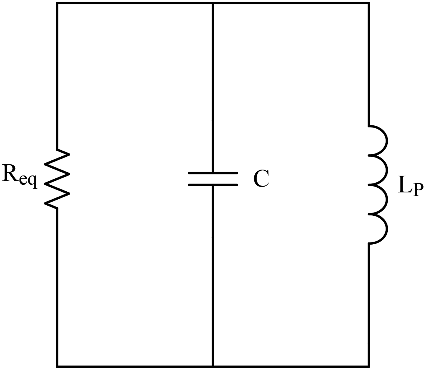
Thus, we can deduce the equivalence model for conversion to parallel, as shown in Figure 11(b). Owing to the high Q, equation (29) can be simplified to obtain L p = L s . This can be further simplified as shown in Fig. 12.
VCO equivalent is the equivalent circuit of the “parallel resonance” form.

Next, equation (30):
 $$R_{eq}=\displaystyle{{ - R_{act} R_P } \over {R_P - R_{act} }}\comma \; $$
shows that when R act exceeds R p , R eq is positive, and the circuit will not oscillate. On the other hand, when R act is smaller than R p , R eq is negative, meeting the conditions for oscillation. Equation (31) is the g m relation:
 $$g_m=\sqrt {2\mu C_{ox} SI_D }\comma \; $$
where μ is the carrier mobility (cm2/V-s), C ox is the unit area of the gate oxide capacitance (F/cm2), and S is the width/length ratio.
Bringing equations (31) into (30) obtains an oscillating relationship which can calculate the following:
 $$I_{D\comma {\rm min}}=\displaystyle{{Q^2 } \over {\mu C_{ox} S\lpar \omega L\rpar ^2 \lpar Q^2+1\rpar ^2 }}.$$
Equation (32) calculates the minimum current needed to produce oscillation. The actual Q value shown in Fig. 13 is about 5, and the method proposed in [Reference Neihart and Harrison5] can be used to increase the Q value. This relationship indicates that a larger width/length ratio will allow for smaller current operation. This result is with agreement with the large transistor selected in the previous section and operation in the MOS subthreshold region.
Inductor Q value (the unit in × label is MHz).

IV. EXPERIMENTAL RESULTS AND DISCUSSION FOR THE MICS FREQUENCY BAND LOW-POWER VCO
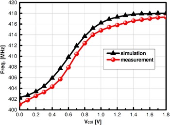
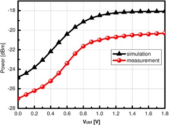
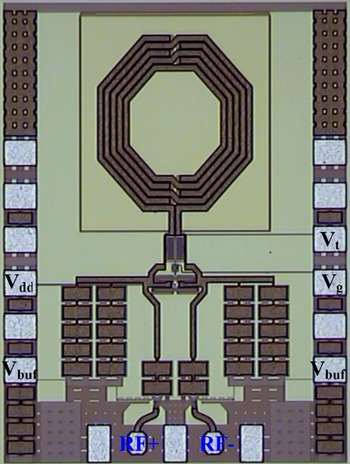
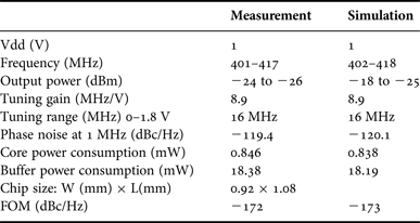
The measurement environment is the wafer surface directly under the probe, using an E5052A signal source analyzer (SSA) to measure the circuit's output spectrum, oscillation frequency, phase noise, and tuning range. The output end uses an open drain buffer amplifier as the measurement buffer, which was connected to the DC T-connection during measurement to give the buffer bias current. Figure 14 shows the oscillation frequency spectrum, where the voltage can be adjusted to 0 V. Figure 15 compares the adjustable range measurement results and the simulation results, where the voltage can be adjusted between 0 and 1.8 V. Figure 16 compares the relationship between adjustable voltage output and output power with the simulation results. Figure 17 shows the phase noise measurement results, where the adjustable voltage is 0 V. Figure 18 shows the chip layout. Table 2 summarizes the simulation and test results for the MICS frequency band low-power VCO. Table 3 compares the features of the proposed MICS frequency band low-power VCO with several fine prior arts [Reference Young, Mallin and Cross6–Reference Vouilloz, Dehollaini and Declercq11]. The work in [Reference Vouilloz, Dehollaini and Declercq11] concerns the whole receiver design, and therefore lacks the data of VCO. As a result, it is not included in the comparison.
Natural oscillation frequency given adjustable voltage of 0 V.

Comparison of adjustable range measurement and simulation results.

Comparison of the relationship between adjustable voltage and output power and simulation results.

Phase noise for adjustable voltage of 0 V.

Chip layout.

Simulation and experimental results for the MICS frequency band low-power VCO.
FOM = Phase noise (dBc/Hz) − 20log(fo/Δf) + 10log(P DC /1 mW).
Feature comparison of the MICS frequency band low-power VCO.

*FOM = Phase noise (dBc/Hz) − 20log (fo/Δf) + 10log(P DC /1 mW).
The circuit design is largely consistent with the simulation, but the Figures of merit (FOM) indicator is insufficiently high primarily because this indicator has a greater impact on the phase noise. In addition, due to the very-low power consumption design, the components operate in the subthreshold region. Therefore, the output power limit is restricted by the low power consumption, thus the output signal power is low. We know that the size of the power output signal is inversely proportional to the phase noise, which is disadvantageous in terms of the oscillator's FOM indicator, leading to a low FOM value. Despite a bit low FOM, our design is quite competitive with those demonstrated in the literature in terms of phase noise. The proposed VCO has three favorable features. First, it has been designed to possess the N-P cross-coupled architecture to increase the equivalent transconductance of VCO under a given DC current. Second, its transistor aspect ratios of the N-P cross-coupled architecture providing transconductance of the VCO have been increased in order to operate them in the subthreshold regime. Third, the gm/I D ratio has been optimized such that the overall power consumption can be maximally reduced. The increase in the transconductance reduces the transistor thermal noise effectively, thereby making our design better than those sub-mW prior works in the phase noise.
V. CONCLUSION
A VCO design has been proposed and implemented in the standard CMOS technology. The main feature is its low-power consumption suitable for wireless medical sensor network applications with MICS band. The VCO can be operated at “μW” DC power consumption with satisfactory phase noise performance. By taking the advantage of proposed current-starved structure, the subthreshold operation can be achieved. Experimental results show that the VCO dissipated about 0.846 mW, with a phase noise of −119.4 dBc/Hz at the main frequency of 1 MHz. Its tuning range is 16 MHz, covering the entire range of 402–405 MHz. Proposed has the FOM of −172. The results justifying our work suggest that it is quite competitive with those currently demonstrated in the literature. We have detailed the design philosophy and chip measurement given as proof of concept. By integrating the proposed VCO with the miniaturized integrated core circuits, it is believed that the life span of battery can be extended and the heat dissipated can be minimized to maximally reduce the risk of damaging the surrounding tissues or cells.
ACKNOWLEDGEMENTS
This study was supported by the National Science Council (NSC), Taiwan, and Ministry of Science and Technology (MOST), Taiwan, under Grants MOST 103-2221-E-182-070-, NSC 102-2218-E-182-003-, MOST 103-2815-C-182-012-E. It is also supported in part by the Chang Gung University (CGU) and Chang Gung Memorial Hospital (CGMH) under Contracts UERPD2D0051 and CMRPD3D0221.The Project was supported, in part, by Zhejiang Provincial Natural Science Foundation of China (Grant No. LQ12F01005).
CONFLICT OF INTEREST
None.
 Cihun-Siyong Alex Gong has been involved in biomedical circuits and systems since starting his M.S. program. He received the B.S. degree in Civil Engineering, the M.S. degree in Biomedical Engineering, and the Ph.D. degree in Electrical Engineering, in 2002, 2005, and 2008, respectively. In 2009, he joined the Industrial Technology 662 Research Institute, Hsinchu, Taiwan, as one of the Research and Development Staff Members. He held Adjunct Assistant Professor positions at National Taiwan Normal University, Taipei, Taiwan, and National United University, Miaoli, Taiwan, in 2012 and 2013, respectively. He joined the Department of Electrical Engineering, School of Electrical and Computer Engineering, College of Engineering, Chang Gung University, Taoyuan, Taiwan, in 2013, where he is currently an Assistant Professor and with the Portable Energy System Group, Green Technology Research Center. His research interests are in electronics for medicine and healthcare, including interfacing-associated solid-state circuits and their physiological issues. He chaired the sessions on Advanced Circuit and System on Green and Biomedical Applications, Information and Communication Technology for Translational Medicine and Green Applications, and RF and Wireless for the IEEE ISCE 2013, the IEEE ICCE-TW 2014, and the IEEE ICCE 2015, respectively.
 Yu Lin Tsou received the M.S. degree in Electrical Engineering from National Central University, Zhongli, Taiwan, in 2004 and 2006, respectively. He is currently pursuing the Ph.D. degree in Communication Engineering at National Chiao Tung University, Hsinchu, with a focus on ultralow-power RF system for WSN applications. He was with the Department of Low Power Mixed Signal, Industrial Technology Research Institute, Hsinchu, Taiwan, where he was involved in designing ultralow-power analog and RF IC.
 Yan-Hsien Yang received his M.S. degree in Electrical Engineering from National Central University, Taiwan, in 2008. He is currently a Senior IC Design Engineer in RF and wireless technologies.
 Hwann-Kaeo Chiou was born in Taichung, Taiwan, in 1959. He received the B.S. degree in Electrical Physics from the National Chiao Tung University, Hsinchu, Taiwan, and the M.S. and Ph.D. degrees in Electrical Engineering from the National Taiwan University, Taipei, Taiwan, in 1982, 1985, and 1997, respectively. He was an Associate Researcher with the Chung-Shan Institute of Science and Technology (CSIST), Taoyuan, Taiwan, from 1985 to 2000, where he was in charge of the development of microwave integrated circuits (MICs) and MMICs, and microwave subsystems for mobile communication. From 2000 to 2002, he was an Associate Vice President with BenQ Inc., Taipei, where he was in charge of the development of broadband wireless access technology. Since 2002, he has been with the faculty of the Department of Electrical Engineering, National Central University, Jhongli, Taiwan, where he is currently a Distinguished Professor. His current research interests include RF integrated circuits, MMICs, and millimeter-wave integrated circuits.
 I-Chyn Wey was born in Taipei, Taiwan, R.O.C., in 1979. He received his B.S. and M.S. degrees in Electronics Engineering from Chang Gung University, Taiwan, in 2001 and 2003, respectively. In 2008, he received the Ph.D. degree in Electronics Engineering from National Taiwan University. He is now an Associate Professor in the Electrical Engineering Department, Chang Gung University. His research interests include VLSI CMOS circuits, noise-tolerant CMOS circuits, near-threshold-voltage CMOS circuits, and ultra-low power CMOS circuits design.
 Meng-Tsan Tsai received his Ph.D. degree from Institute of Photonics and Optoelectronics, National Taiwan University, Taipei, Taiwan, in 2008. He worked as a postdoctor fellow in the same institution for 1 year after his graduation. He is currently an associate professor in the Department of Electrical Engineering, Chang Gung University, Taoyuan, Taiwan. His research interests include biophotonics and optics design.
 Changhong Yu received the Ph.D. degree in Information and Communication Engineering from Zhejiang University, China, in 2007. Now he is working in College of Information and Communication Engineering at Zhejiang Gongshang University. He has worked with Jie Chen from BINARY lab (Biology, Information science and Nanotechnology Applications and Research laboratory) (Alberta, Canada) since 2005. He has taken part in the design of cost-efficient MRF circuit. His interests include fault tolerance circuit design and optimization of CMOS system circuits. Currently, he focuses on self-recovery fault tolerant clock circuit.
 Ling-ling Lin was born in Xiapu, Fujian, in 1990. She received the B.S. degree in the Measurement and Control Technology and Instrument and the M.S. degree in Electronic and Information Engineering from ZJGSU, Hangzhou, Zhejiang, in 2012 and 2015, respectively. From 2012 to 2013, she was engaged in research of intelligent monitoring at Information and Electronic engineering Laboratory, in ZJGSU, Hangzhou. From October 2013 to August 2014, she went to CGU for exchange learning, in Taiwan. In this period, she studied in VLSI architectures. Now, she is engaged in the research of digital image processing.