Introduction
Organic materials, primarily composed of carbon, hydrogen, and oxygen, are insulators and have very high resistivity at room temperature. Organic molecules with sp 2 hybridization and delocalized π-electrons, such as conjugated hydrocarbons, metal phthalocyanines, and oligothiophenes, have semiconducting properties.Reference Wang, Dong, Hu, Liu and Zhu1 Organic charge-transfer compounds, based on organic donors and acceptors,Reference Ishiguro, Yamaji and Saito2 might become conducting or even superconducting. These extraordinary properties, which are unexpected in conventional non-conjugated organic materials, make organic semiconductors the subject of intense recent exploration.
Organic semiconducting thin films are used in numerous applications such as organic field-effect transistors (OFETs),Reference Klauk3 organic light-emitting diodes (OLEDs),Reference Kulkarni, Tonzola, Babel and Jenekhe4 and organic solar cellsReference Hoppe and Sariciftci5 because of their light weight, flexibility, material solubility, low-temperature processability, large-scale yields, and low cost. Spin coating, drop casting, or printing techniques can be applied in the production of prototype electronic devices. However, grain boundaries,Reference Horowitz and Hajlaoui6 defects,Reference Kalb, Meier, Mattenberger and Batlogg7 dislocations,Reference Chapman, Checco, Pindak, Siegrist and Kloc8 and impuritiesReference Rep, Morpurgo, Sloof and Klapwijk9 make polycrystalline organic films not suitable for the investigation of the intrinsic properties of organic semiconductors. Instead, organic single crystals that can be prepared with high purity and low density of defects are ideal model compounds.Reference de Boer, Gershenson, Morpurgo and Podzorov10–Reference Li, Hu, Liu and Zhu13 They can be used to investigate structure-performance relationships,Reference Yang, Wang, Wang, Long and Shuai14 intrinsicReference Podzorov, Menard, Borissov, Kiryukhin, Rogers and Gershenson15 and anisotropicReference Sundar, Zaumseil, Podzorov, Menard, Willett, Someya, Gershenson and Rogers16 properties, and photoconductivities,Reference Najafov, Lee, Zhou, Feldman and Podzorov17, Reference Jiang, Yang, Cui, Liu, Li and Hu18 and can be used in computational simulations and calculations.Reference Hannewald and Bobbert19, Reference Ortmann, Bechstedt and Hannewald20 Some potential applications for organic single crystals include inverters,Reference Jiang, Hu, Wei, Xu and Meng21 logic circuits,Reference Tang, Tong, Hu, Wan and Bjørnholm22 and sensors.Reference Jiang, Zhao, Zhang, Chen, Kloc and Hu23
Van der Waals forces exist in organic semiconductors, and these weak intermolecular interactions give rise to different properties in organic semiconductors compared to inorganic semiconductors in which metallic or covalent bonds are predominant. The physical properties of organic semiconductors differ substantially from inorganic semiconductors. Melting points and sublimation temperatures are mostly much lower in organic semiconductors; therefore the methods of crystal growth of organic semiconductors are also substantially different from those used for inorganic materials.
Many semiconducting organic molecules have been synthesized thus far, but only a few have been processed into solid samples for electrical charge transport measurements, and even fewer have been crystallized into freestanding single crystals large enough for electrical measurements. For electrical measurements, single crystals a few micrometers in size have to be formed directly on prepared surfaces.Reference Briseno, Mannsfeld, Ling, Liu, Tseng, Reese, Roberts, Yang, Wudl and Bao24–Reference Jiang, Zhang, Ye, Wei, Hu, Guo, Liang, Chen, Zhao, McNeil, Hu and Kloc32 Single crystals that are a few tenths of a micrometer in size are required for structure determination. Therefore, a large number of organic crystal growth methods have been developed, and most have been based on modified inorganic crystal growth methods.
In this article, solution, gas-phase, and melt-growth methods for organic single-crystalline semiconductors are discussed, with the aim of preparing specimens that provide insights into the intrinsic properties of organic semiconductors. The nature of the individual molecules and the interactions between molecules determine which growth method is preferred for particular materials.
Solution growth method
Most organic molecules are soluble in organic solvents over a range of temperatures and pressures. This behavior makes it possible to use solubility for the crystal growth of large molecular weight molecules, which decompose into small molecules during the sublimation process. Based on the properties of a given organic molecule, several solution methods are available.
Solvent evaporation method
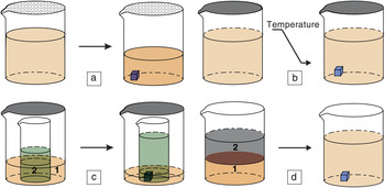
The solvent evaporation method is the simplest and most effective method to grow single crystals, and most organic crystals used for crystal structure analysis are grown by this method. Organic solvents, such as dichloromethane, chloroform, toluene, benzene, and chlorobenzene are used (Figure 1a). If a beaker containing a saturated solution is not covered too tightly, the solvent can slowly evaporate forming supersaturated solution. Then nuclei (seeds) spontaneously form, growing into larger crystals. As the solubility of some organic semiconductors, for example, tetrathiafulvalene (TTF) and its derivatives, in certain organic solvents is very high, the drop casting method is preferred. This method is a type of solvent evaporation method and widely applied for the fabrication of single-crystalline films for field-effect transistor measurements. Single-crystalline film of TTF and its derivatives can be obtained by directly pouring n-heptane or chlorobenzene saturated solutions onto prefabricated substrates. Crystallization occurs once the solvent evaporates, and mobilities greater than 1 cm2 V–1 s–1 are reported.Reference Mas-Torrent, Durkut, Hadley, Ribas and Rovira29–Reference Pfattner, Mas-Torrent, Bilotti, Brillante, Milita, Liscio, Biscarini, Marszalek, Ulanski, Nosal, Gazicki-Lipman, Leufgen, Schmidt, Molenkamp, Laukhin, Veciana and Rovira31 It is worth noting that millimeter-sized single-crystal monolayers of 1,4-bis((5’-hexyl-2,2’-bithiophen-5-yl)ethynyl)benzene (HTEB) can be obtained by drop casting, which show high mobilities up to 1 cm2 V–1 s–1.Reference Jiang, Dong, Meng, Li, He, Wei, He and Hu27 In addition, some polymers, such as poly(3-hexylthiophene) (P3HT), can also be deposited by the solution evaporation method.Reference Kim, Han, Park, Jang, Cho, Hwang and Cho33
Solution-based methods for the growth of organic semiconductor single crystals. (a) Solvent evaporation method. Molecules crystallize due to increased concentration resulted from solvent evaporation. (b) Slow cooling method. Molecules crystallize due to a decrease of solution solubility in low temperature. (c) Vapor diffusion method. Molecules crystallize because solvent 1 evaporates and diffuses into solvent 2, leading to an oversaturated solution. (d) Liquid–liquid diffusion method. Molecules crystallize because solvent 1 interdiffuses with solvent 2 and results in a decrease of solution solubility in solvent 2.

Slow cooling method
The slow cooling method is suitable for organic semiconductors whose solubility in organic solvents is moderate at room temperature but changes considerably with temperature (Figure 1b). As the temperature increases, more organic semiconductor material can be dissolved in solution until a saturated solution forms. When the temperature of the saturated solution slowly decreases, organic semiconductor material spontaneously forms nuclei and additional material deposits onto the seeds, and large crystals are obtained. The process can be repeated several times, oscillating the temperature around the saturation temperature in such a way that only a small portion of material dissolves and crystallizes in the following temperature oscillation period. This process results in preferred dissolution of the smallest seeds and crystallization on the remaining seeds. In this way, large organic crystals, even mm-sized, can be formed. Thin rubrene single crystals can be obtained by this method with a solvent of 1-propanol, and the attained mobility can be up to 1.6 cm2 V–1 s–1.Reference Matsukawa, Yoshimura, Sasai, Uchiyama, Yamagishi, Tominari, Takahashi, Takeya, Kitaoka, Mori and Sasaki34 The solvent evaporation method can be combined with the slow cooling method to obtain even larger organic crystals.
Vapor diffusion method
The vapor diffusion method (Figure 1c) is used to grow organic semiconductors that are highly soluble in a particular organic solvent (“good” solvent) but have poor solubility in other solvents. Organic semiconductors are dissolved in a “good” solvent that has a low vapor pressure to form a saturated solution. The beaker containing the saturated solution is then placed in a larger beaker that contains a volatile solvent that only slightly dissolves the organic semiconductors. When the larger beaker is sealed, the volatile solvent evaporates, and the gas diffuses into the saturated solution of organic semiconductors, leading to an oversaturated solution. Then nucleation and crystallization occur. The gas diffusion speed can be regulated by adjusting the solution temperature.
The vapor diffusion method works well to generate small amounts of organic semiconductors. Moreover, by selecting only a few seeds, tetrathiafulvalene-tetracyanoquinodimethane (TTF-TCNQ) with mm-sized crystals were formed when the crystal growth parameters were carefully controlled.Reference Johannsen, Groth-Andersen and Nielsen35
Liquid–liquid diffusion method
Two layers of different solvents are used in the liquid–liquid diffusion method, and the solubility of the crystallizing material in these two solvents is different. As shown in Figure 1d, the organic semiconductor is dissolved in the high-solubility solvent to form a saturated solution. The low-solubility solvent diffuses into the high-solubility solvent layer, causing the formation of a saturated solution at the interface between the solvent layers. For example, a single-crystalline micro-ribbon of triisopropylsilylethynyl pentacene (TIPS-PEN) can be grown by this method using toluene as the high-solubility solvent and acetonitrile as the low-solubility solvent.Reference Kim, Lee, Lee, Lee, Kim, Han and Cho36 The liquid–liquid diffusion method generates high-quality small crystals, mostly micrometer sized, because the crystals are growing at the solvent interface without any stress from substrates.
Organic flux solid solvent method
Organic semiconductors, such as metal phthalocyanines, have high melting points and sublimation temperatures above 500°C; and perylene derivatives usually decompose at a temperature near its melting point. These types of organic semiconductors are difficult to dissolve in most organic solvents, and an organic solid solvent method is used to grow large crystals of these materials. Generally, an organic material that is solid at room temperature, such as anthracene, can be used as a solvent at temperatures above its melting point and can dissolve other molecules that are not soluble at low temperatures. For example, when a mixture of anthracene and copper phthalcyanine (CuPc) powders is heated, the anthracene melts and dissolves the CuPc. Then, when the temperature slowly decreases, black needle crystals of CuPc form and can be separated from the solid anthracene by adding an organic solvent, such as toluene.Reference Miyahara and Shimizu37
Supercritical solvent method
Supercritical fluids can be used as solvents to precipitate large molecules. For example, supercritical CO2 can act as an antisolvent to control the precipitation of C60 crystals from solution. In the experiment, C60 dissolves in toluene to form a saturated solution, which is then injected into supercritical CO2. CO2 quickly reduces the solvent power of toluene, and C60 precipitates.Reference Field, Hamley, Webster, Gregory, Titman and Poliakoff38
Physical vapor transport method
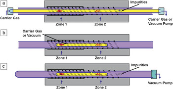
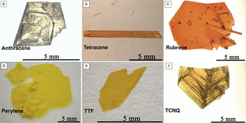
Most of the organic semiconductors have relatively low melting points and low sublimation temperatures. Purification of these organic semiconductors is usually performed using high-vacuum evaporation. However, during this process, lightweight impurities sublime and condense together with the desired material on the same substrate. The physical vapor transport (PVT) method was developed to separate the organic semiconductors from these impurities.Reference Piper and Polich39–Reference Laudise, Kloc, Simpkins and Siegrist41 The method combines crystal growth with material purification, with several different PVT methods frequently employed: open systems (Figure 2a), closed systems (Figure 2b), and semi-closed systems (Figure 2c). The open and closed systems include a vacuum or an inert gas environment. Some typical organic crystals grown by PVT methods are shown in Figure 3.
Scheme of the physical vapor transport growth method. (a) Open system. The material is heated in zone 1 and sublimed in a flow of carrier gas under pressures ranging from a few Torr (few hPa) to atmospheric pressure. The molecular vapor crystallizes downstream at a lower temperature in zone 2, with pure crystals separated from impurities due to the temperature gradient and the flow of the carrier gas. (b) Closed system. The material (impurities and the compound of interest) is heated in a sealed glass/quartz ampoule. (c) Semi-closed system. The materials are sealed in a glass ampoule, but a small orifice in the ampoule allows impurities and a portion of the crystallizing material to escape from the ampoule. Zone 1: Sublimation zone; zone 2: Crystal growth zone.

Representative organic single crystals grown by the physical vapor transport method: (a) anthracene (C14H10), (b) tetracene (C18H12), (c) rubrene (C42H28), (d) perylene (C20H12), (e) tetrathiafulvalene (TTF, C6H4S4), and (f) 7,7,8,8-tetracyanoquinodimethane (TCNQ, C12H4N4).

PVT in an open system
In an open system, an inert gas controls the speed of sublimation, deposition, and crystal growth of organic molecules. Organic semiconductors and impurities are deposited in different locations because of their different molecular weights. In addition, the inert gas functions as a protective gas that prevents oxidation of the organic semiconductors.
Organic molecules are linked by weak van der Waals forces, and the growth units are single molecules. To undergo crystallization, organic molecules must obtain extra energy to reconstruct, link to each other, and form an initial crystal surface. In fact, some organic semiconductors cannot crystallize in high vacuum, but they can form beautiful crystals in the presence of inert gases. Rubrene, for example, forms quasi-amorphous, disordered films during thermal evaporation under high vacuum conditions, because free non-interacting rubrene molecules undergo a twisting conformation that hampers crystallization.Reference Käfer and Witte42 The field-effect mobility of such thin films is low because of their amorphous nature.Reference Park, Hwang, Choi, Hwang, Oh, Kim and Im43 However, under inert gas conditions, rubrene can form large red single crystals (Figure 3c) several centimeters in size. The maximum reproducible intrinsic mobility in these crystals ranges from ∼5 to 20 cm2 V–1 s–1, depending on the dielectric constant of the material used as a gate insulator in OFETs (for ε = 1–4).Reference Podzorov, Menard, Borissov, Kiryukhin, Rogers and Gershenson15, Reference Podzorov, Sysoev, Loginova, Pudalov and Gershenson44 Hydrogen, argon, and nitrogen gases are usually used in the PVT method. However, there are only a few reported studies that discuss the role of the gas on organic semiconductor charge-carrier mobilities.
Temperature control is very important for the single-crystal growth of organic semiconductors. The sublimation temperature is usually set near the melting point of the desired material, and the temperature gradient needs to be adjusted for a particular material.Reference Jiang, Tan, Zhang, Chen and Kloc45, Reference Tang, Jiang, Tong, Li, Liu, Wang, Hu, Liu and Zhu46
PVT in a closed and a semi-closed system
In a closed system, the source materials are sealed in a quartz ampoule under vacuum or inert gas conditions, and neither reactants nor products can escape from the ampoule during crystal growth. Crystals of anthracene, pyrene, naphthalene, and C60 have been grown in closed systems.Reference Dhanaraj, Byrappa, Prasad and Dudley47 In closed systems, even if very pure source materials are used, some new molecules may still form because of decomposition, photoreaction, polymerization, or chemical reactions that occur during the crystal growth process. To remove contaminants, a semi-closed system (Figure 2c) has been developed. In this method, one end of the furnace tube is sealed, and the other end is connected to a high-vacuum pump, which removes volatile impurities. The crystallization of urea crystals has been performed in a semi-closed system; detailed studies of urea crystal growth are helpful indicators for the growth of organic semiconductors with vapor pressures similar to urea.Reference Feigelson, Route and Kao48
Melt growth method
The melt crystal growth methods, such as Czochralski, Bridgman, or floating zone methods, are most frequently used for growing large crystals of inorganic semiconductors. Owing to the high vapor pressure and chemical instability of large organic molecules of organic semiconductors around melting temperatures, the melt growth approach has been explored only for a few organic molecules that are inexpensive and available in larger quantities. Naphthalene,Reference Selvakumar, Sivaji, Arulchakkaravarthi, Balamurugan, Sankar and Ramasamy49 anthracene,Reference Probst and Karl50 phenanthrene,Reference McArdle, Sherwood and Damask51 pyrene,Reference Inokuchi52 tetracene,Reference Niemax and Pflaum53 and stilbeneReference Arulchakkaravarthi, Santhanaraghavan and Ramasamy54 have been grown from melts. These molecules are relatively stable at the melting temperature but may polymerize or decompose during long heat treatments or under intense light. For a few materials,Reference Selvakumar, Sivaji, Arulchakkaravarthi, Balamurugan, Sankar and Ramasamy49–Reference Arulchakkaravarthi, Santhanaraghavan and Ramasamy54 large high quality single-crystalline ingots were obtained. Mostly, however, crystallization from the melt is difficult, and a material that has a strong tendency to evaporate during melting requires significant modifications to organic crystal growth methods.
Bridgman growth method
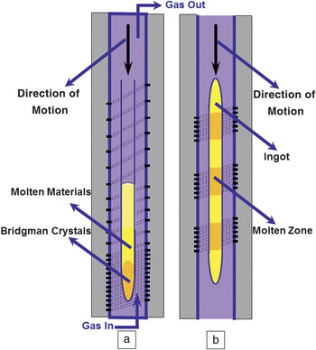
The Bridgman growth method is used for the growth of large single crystals inside sealed ampoules.Reference Bridgman55 In this method (Figure 4a), a quartz ampoule is filled with powdered material. The ampoule is sealed under vacuum or with an inert gas, and then moves through a temperature gradient. At a certain temperature, crystal nucleation is induced at the tip of the ampoule, and the crystallization front propagates through the melted material.
(a) Bridgman and (b) zone melting methods used for organic single crystal growth. In both methods, material is melted in an ampoule, and crystallization proceeds from one end of the ampoule during motion of the melt–crystal interface. In the Bridgman method, the whole ingot is melted, and crystallization begins from the tip of the ampoule where a seed or spontaneously formed nucleus is located. In the zone melting method, only one or a few narrow zones are melted, and the crystal–melt interfaces move with the temperature gradient. In both methods, the impurities are segregated at the crystal–melt interface, resulting in purification of the forming crystal.

The ampoule moves slowly across the temperature gradient, and as the solubility of many impurities in the melt is different from the crystal solubility, the deposited impurities are separated from the crystals.Reference Brissaud, Dolin, Leduigou, McArdle and Sherwood56 However, if the solubility of the impurities in the melt is almost the same as that in the crystals, impurities cannot be removed by this method.
As the Bridgman method uses a sealed ampoule, chemical purification is less efficient. Therefore, purification needs to be carried out in a separate process before crystal growth. After meticulous purification and optimal growth conditions, the electrical properties of large Bridgman-grown organic semiconductor crystals may match gas-phase-grown small crystals. A high-quality single crystal of 9,10-diphenylanthracene (DPA), grown by the Bridgman method, exhibited a time-of-flight electron mobility close to 13 cm2 V–1 s–1 and a hole mobility of 3.7 cm2 V–1 s–1 at room temperature.Reference Tripathi, Heinrich, Siegrist and Pflaum57
The Bridgman growth method can produce large crystals, limited only by the dimensions of the ampoules used for crystallization, but the strain at the boundary between the crystal and the quartz walls of the ampoule can induce cracks, stress, or small angle grain boundaries in the crystals.
Zone melting growth method
The zone melting growth method (Figure 4b) differs from the Bridgman growth method in that it employs a series of short heating elements. Impurities melt in the narrow molten zones, and purer crystalline material accumulates outside the molten zone.
The zone melting growth method has been used for the purification of large amounts of organic semiconductors, such as anthracene, naphthalene, and perylene.Reference Karl58, Reference Hong, Tan, Toh, Jiang, Zhang and Kloc59 Very high purity has been achieved, but because of the repeated melting of the material, this time consuming method has only been applied to these few materials.Reference Karl58, Reference Hong, Tan, Toh, Jiang, Zhang and Kloc59
Czochralski growth method
The Czochralski growth method is usually used for growing inorganic crystals. As an open crucible is used to melt the material, the evaporation of molecules during crystal pulling makes this method applicable to a only a few materials, such as benzophenone and benzil.Reference Bleay, Hooper, Narang and Sherwood60, Reference Arivanandhan, Sankaranarayanan, Sanjeeviraja, Arulchakkaravarthi and Ramasamy61 In this method, organic powders melt in a crucible, and a rotating small crystal seed is slowly immersed and then pulled out of the melt. The crystal grows along the small seed, and the growth direction of the crystal and the seed is the same. However, the Czochralski growth method has not been used for typical organic semiconductors, and the behavior and purity of grown crystals needs more attention.
Growth of binary semiconducting compounds
Binary compounds formed from acceptor-donor charge-transfer compounds show semiconducting, conducting, or even superconducting behavior.2 The crystal growth methods of binary organic compounds are similar to the crystal growth methods of individual molecules. The binary phase diagrams of organic compounds, however, have rarely been studied, and, therefore, very little is known about the stoichiometry, polymorphism, or melting properties of such compounds. Perylene and 7, 7, 8, 8-tetracyanoquinodimethane (TCNQ) form three compounds: (perylene)1-TCNQ (P1T1), (perylene)2-TCNQ (P2T1), and (perylene)3-TCNQ (P3T1).Reference Tickle and Prout62, Reference Truong and Bandrauk63 The crystals are grown from the gas phase by the PVT growth method or from solvents, but the control of the stoichiometry in such compounds is not well understood.
Conclusions
Synthetic organic chemistry offers a powerful tool for preparing a large number of new molecules rich in delocalized π-electrons. Using various methods, material scientists can transform individual molecules into crystalline materials suitable for measurements or for use in applications. Organic single crystals are ideal model compounds that can reveal the intrinsic properties of organic semiconductors. Many methods have been developed to purify the source materials and grow organic single crystals. The solution method is often used for organic semiconductors that have good solubility in organic solvents. The physical vapor transport method is suitable for organic semiconductors that sublime without decomposition; this method can generate very high-quality organic molecular crystals. The Bridgman growth method is applied to organic semiconductors that have low melting points and do not decompose. Very large Bridgman crystals can be obtained and are used for time-of-flight measurements. The Czochralski growth method has a small application range but results in better-quality organic crystals. Different crystal growth approaches should be selected depending on the organic semiconductor of interest.
Currently, researchers have found few organic semiconductors applicable for “plastic electronics.” However, the potential of synthesizing new complex molecules and forming binary and multinary compounds seems unlimited. Crystal growth, which is a slow and time consuming method, is inadequate for the evaluation of such a large number of new semiconductors. However, it may be speculated that future progress in computational methods will allow for the selection of a few best organic semiconductors, and then the single-crystal growth methods will be the methods of choice for studying the fundamental properties of these materials.
Few studies have focused on investigating the crystal quality of organic semiconductors. The interdependence between the purity, defect density, and grain boundaries in organic semiconductors seems to affect their charge transport and optical properties. However, this dependence is complex, and improvements in an individual parameter such as purity do not promise an improvement in the desired physical properties. For example, the mobility of pentacene measured in polycrystalline thin films may be as high as or even higher than the mobility measured in single crystals. However, pentacene undergoes a structural phase transition between the single-crystal growth temperature and room temperature, where the mobility measurements are conducted. Likely, the intrinsic mobility of pentacene is still unknown, and current mobility measurements are limited by defects and impurities. Therefore, studies of organic single crystals and, in particular, the growth of these organic single crystals that precede physical properties measurements should be given more attention in order to deepen our understanding of the fundamental materials properties and device physics of organic semiconductors.
Acknowledgments
The authors acknowledge financial support from Nanyang Technological University (NTU-BGU-HU NRF CREATE program, Nanomaterials for Energy and Water Management, M59070000). The authors thank Dr. Te Ba (Nanyang Technological University) for his critical discussion of the manuscript.