Introduction
To increase the lifetime of tooling or engineering components, it is necessary to protect them from environmental impacts, chemical attacks, and adverse influences arising from high-temperature applications. One well-established way to achieve this goal is by protective coatings such as nitrides, carbides, and borides of transition metals (TM). While the production of wear- and corrosion-resistant hard materials based on nitrides[Reference PalDey and Deevi1] and carbides[Reference Kumar, Kumar, Kalaiselvam, Radhika, Maximus Rabel and Jayavel2] is well-accepted, the industrial application of thin films based on borides is rather limited.[Reference Mitterer, Waldhauser, Beck and Reiners3, Reference Chrzanowska-Giżyńska, Denis, Hoffman, Giżyński, Mościcki, Garbiec and Szymański4]
Due to the fact that transition metal borides (TMB) have highly attractive properties like chemical stability,[Reference Nedfors, Mockute, Palisaitis, Persson, Näslund and Rosen5] high hardness,[Reference Lee, Chen, Chung and Keer6] and good electrical and thermal conductivity,[Reference Shibuya, Kawata, Ohyanagi and Munir7] this material class is highly interesting for application-oriented coating developments. Although, TMBs show a high stoichiometric variety,[Reference Mori8] especially diborides tend to have outstanding mechanical properties.[Reference Mayrhofer, Kirnbauer, Ertelthaler and Koller9] Representatives of the TMB2 material system that show extraordinary characteristics are, for example, TiB2 (hardness values up to 70 GPa) and MgB2 (high-temperature superconductor with a critical temperature of 39 K).[Reference Nagamatsu, Nakagawa, Muranaka, Zenitani and Akimitsu10]
Latest studies on diborides show that the compounds prefer to crystallize mainly in two related hexagonal structures: AlB2 structure type (α, space group 191––P6 mmm−1) favored by early TM diborides or W2B5−x-based structure (ω, space group 194––P63 mmc−1) preferredly formed by late TMB.[Reference Moraes, Riedl, Fuger, Polcik, Bolvardi, Holec and Mayrhofer11] A characteristic for the AlB2 structure type is the hexagonal-shaped unit cell with alternating stacking of covalent bonded boron hexagons and metal layers. The W2B5−x structure also consists of a hexagonal unit cell but with alternating flat and puckered boron layers between the metal layers.
The chemical stability of the various TMB2 in the α-structure can be nicely correlated to the number of states at the Fermi level [N(E F)]. TMB2 revealing the lowest N(E F)––where the Fermi level is located in the pseudogap between the bonding and antibonding states––show the highest chemical stability of all α-TMB2 [e.g., TiB2 (3d), ZrB2 (4d), and HfB2 (5d)]. Moreover, the size of the TM-atom in the individual compound is crucial for strains in the B–B bonds influencing the chemical stability.[Reference Vajeeston, Ravindran, Ravi and Asokamani12]
By means of density functional theory (DFT) calculations, WB2 was classified as a ductile material, in its metastable α-structure.[Reference Moraes, Riedl, Fuger, Polcik, Bolvardi, Holec and Mayrhofer11] This highly attractive property of α-WB2 combined with experimental studies showing that WB2 can be captured in its α-structure when deposited as thin film makes this material system highly attractive as a starting point for designing ternary diborides.[Reference Euchner, Mayrhofer, Riedl, Klimashin, Limbeck, Polcik and Kolozsvari13, Reference Liu, Jiang, Pei, Lei, Gong and Sun14] Furthermore, it was shown that point defects such as vacancies [which are typical for physical vapor deposited (PVD) materials] are beneficial for stabilizing the metastable α-structure with its distinct ductile behavior of WB2. However, not only vacancies but also alloying elements can stabilize a metastable structure.[Reference Euchner, Mayrhofer, Riedl, Klimashin, Limbeck, Polcik and Kolozsvari13–Reference Moraes, Fuger, Paneta, Primetzhofer, Polcik, Bolvardi, Arndt, Riedl and Mayrhofer16] In the case of the WB2 material system, Ta is a predicted candidate to support the formation of the metastable structure, with only a minute reduction in ductility.[Reference Moraes, Fuger, Paneta, Primetzhofer, Polcik, Bolvardi, Arndt, Riedl and Mayrhofer16] Energy of formation (E f) data indicate that TaB2 exhibits almost the same chemical stability for both crystal structures (α and ω). Again (as for WB2) the α-structure exhibits a significantly better ductility than the ω-structure, and vacancies would support the formation of α rather than ω.[Reference Moraes, Riedl, Fuger, Polcik, Bolvardi, Holec and Mayrhofer11] Thus, we proposed that α-W1−xTaxB2−z is a promising ternary boride material system combining excellent mechanical strength (as typical for diborides) with outstanding high toughness values. TaB2 helps to promote and extend the metastable α-phase region of WB2 (as already proven also experimentally[Reference Moraes, Fuger, Paneta, Primetzhofer, Polcik, Bolvardi, Arndt, Riedl and Mayrhofer16]) with only minor costs in ductility.
In this study, we further investigate the impact of point defects by means of DFT calculations and investigate the fracture toughness of single-phase α-W1−xTaxB2−z coatings by in situ micromechanical bending tests.
Computational and experimental details
DFT coded VASP (Vienna Ab Initio Simulation Package)[Reference Kresse and Joubert17, Reference Kresse and Furthmüller18] calculations using the projected augmented waves method within the generalized gradient approximation (PAW-PBE)[Reference Perdew, Burke and Ernzerhof19] were applied to study the influence of Ta alloying and vacancies on α- and ω-W1−xTaxB2−z structures. Here, also the impact of Schottky defects (stoichiometric defects) was studied. More precisely we made use of the SQS approach[Reference van de Walle, Asta and Ceder20] creating 3 × 3 × 1 supercells containing 108 atoms for the ω-lattice and 3 × 3 × 3 supercells containing 81 atoms to build up the α-structure. The experimentally obtained chemical compositions of the coatings (exhibiting a clear boron deficiency when using Time-of-Flight Elastic Recoil Detection Analysis, TOF-ERDA), were used to fine-tune our calculations for a better comparison with experiments. Therefore, we calculated α-structured cells with WB1.78 (9.3 at.% B-vacancies), W0.93Ta0.07B1.76 (11.1 at.% B-vacancies), W0.86Ta0.14B1.83 (7.4 at.% B-vacancies), and W0.74Ta0.26B1.87 (5.5 at.% B-vacancies). To meet the experimental chemical composition and consider also stoichiometric Schottky defects, we furthermore studied the impact of B-vacancies plus Schottky defects by using α-structured cells with the same overall chemical composition having 3.7% MeB2 Schottky defects, hence, WB1.78 (3.7 at.% M-vacancies, 13.0 at.% B-vacancies), W0.93Ta0.07B1.76 (3.7 at.% M-vacancies, 14.8 at.% B-vacancies), W0.86Ta0.14B1.83 (3.7 at.% M-vacancies, 11.1 at.% B-vacancies), and W0.74Ta0.26B1.87 (3.7 at.% M-vacancies, 9.3 at.% B-vacancies).
The WB2 and W1−xTaxB2−z coatings were deposited by DC magnetron sputtering using an in-house developed magnetron sputtering system. The coating facility was equipped with two 6 in. (TaB2 and W2B5) powder-metallurgically prepared targets (Plansee Composite Materials GmBH). Prior to the depositions, the silicon (100) (20 mm × 7 mm × 0.33 mm) and sapphire (10 mm × 10 mm × 0.5 mm) substrates were ultrasonically pre-cleaned in acetone and ethanol for 5 min, mounted, and heated up in the chamber to the deposition temperature T dep of 700 °C. Furthermore, the substrates were etched in argon atmosphere (p etch = 6 Pa) for 10 min applying a voltage of −500 V. All thin films were deposited in argon atmosphere (working pressure of 0.4 Pa) and using an applied bias-voltage of −50 V on the rotating substrate holder (f rot = 0.25 Hz). The mean distance between the target and substrate holder is around 108 mm. Both targets were powered by current-driven generators (Solvix HiP3––used in DC mode) applying 4.2 A in total for 60 min in each deposition run. To achieve the full compositional range (0–100 at.% Ta), the current was decreased successively by 10% at one generator and increased by 10% at the second generator. To obtain substrate-free thin film material, for detailed structural characterization by x-ray powder diffraction [XRD, with a Philips XPERT diffractometer in Bragg-Brentano configuration equipped with a Cu-K α (λ = 1.54 Å) radiation source], also AISI steel foil (thickness of 0.05 mm) was used as a substrate within the deposition process. After the deposition process, the foil was dissolved in hydrochloric acid (HCl) to obtain substrate-free coating powder.
To obtain the chemical composition of the W1−xTaxB2 thin films, the specimens were investigated by TOF-ERDA with a recoil detection angle of 45° and a 36 MeV I8+ ion beam. Due to resolution limits of the present metal atoms, the films were additionally investigated by using energy-dispersive x-ray spectroscopy (EDS, FEI Philips XL30 with an EDAX EDS detector, 10 kV accelerating voltage). Scanning electron microscopy (SEM) investigations of fracture cross-sections (coatings on Si substrates) were carried out in a FEI Quanta 200 SEM equipped with a field emission gun. The residual stresses of our as-deposited coatings are obtained using Stoney's equation[Reference Janssen, Abdalla, van Keulen, Pujada and van Venrooy21] (with a NANOVEA PS50 chromatographic, confocal profilometer, we obtained the essential radius of curvature of one-side-coated Si stripes). Nanoindentations were performed with a UMIS Nanoindenter equipped with a Berkovich tip to obtain hardness (H) and indentation modulus (E) by evaluating the indentation curves after Oliver and Pharr.[Reference MANN22] In situ micromechanical bending tests of substrate-free coating cantilevers are performed to obtain the fracture toughness of our coatings. These experiments were performed within an SEM equipped with a pico-indenter (Hysitron PI-85 SEM) whose spherical diamond tip was pressed onto the top of the pre-notched cantilever (in growth direction of our coatings) until fracture. The coating cantilevers were shaped by focused ion beam milling from regions where the Si substrate was locally removed from coated samples via wet chemical etching. Details about the entire procedure, set-up used, and the evaluation are given in Ref. [Reference Bartosik, Hahn, Zhang, Ivanov, Arndt, Polcik and Mayrhofer23]. The data were used for calculating K IC according to the mathematical approach of Matoy et al.[Reference Matoy, Schönherr, Detzel, Schöberl, Pippan, Motz and Dehm24]
Results and discussion
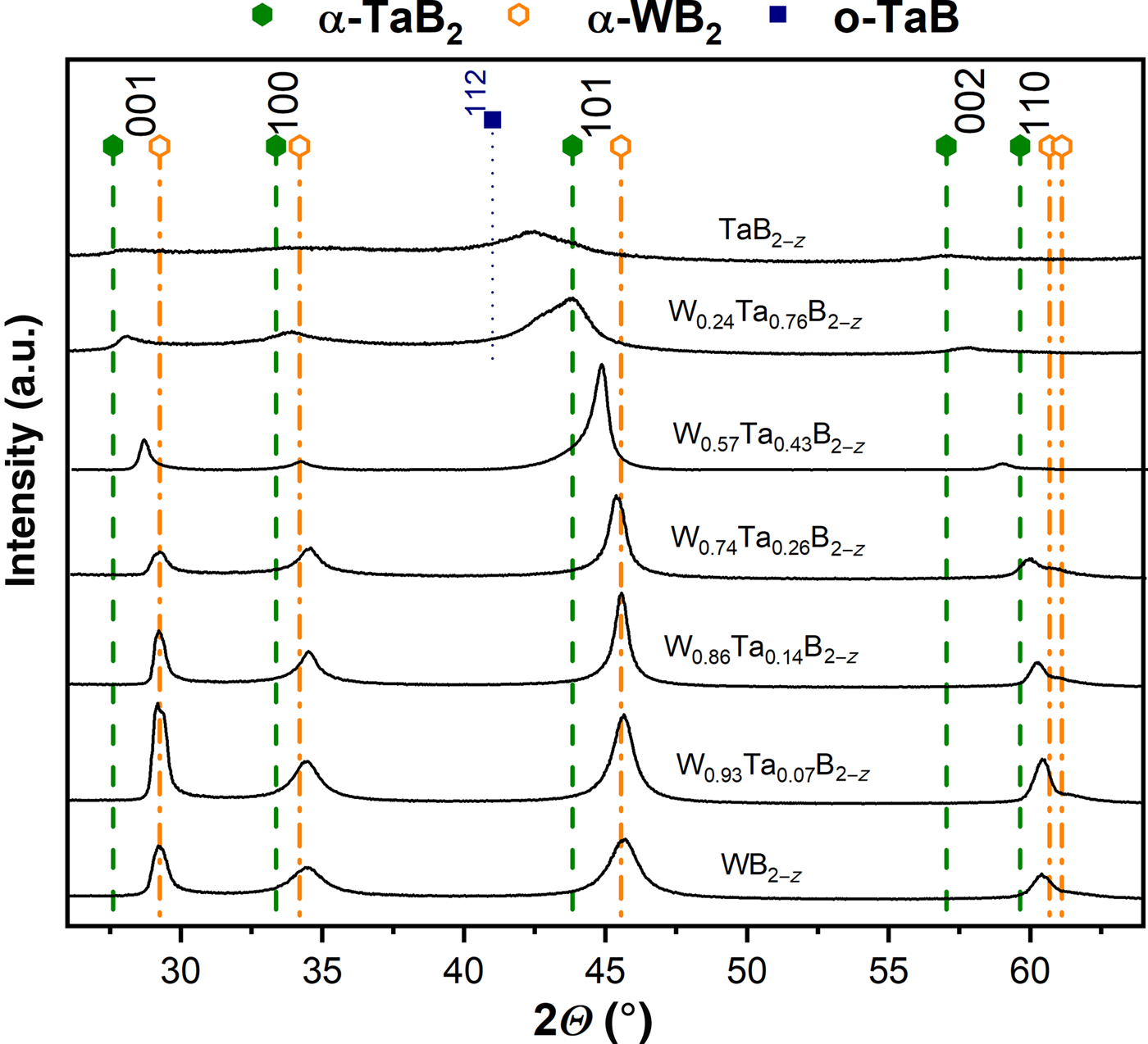
X-ray diffraction of our substrate-free coating powder (see Fig. 1) reveals single-phased α-structured ternary W1−xTaxB2−z solid solutions up to 26 at.% Ta (at the metal sublattice, i.e., x max = 0.26). By further increasing the Ta content (here, Ta = 43 at.%), a small left-hand shoulder formation of the 101 XRD peak (2Θ ~ 46°) develops, indicating the formation of a new phase. This is even more pronounced for the coating containing 76 at.% Ta, where no single-phased structure can be identified and a mixture of α-(Ta,W)B2 and orthorhombic (Ta,W)B is present. The coating prepared from the TaB2 target itself (without adding of WB2) suggests an even more pronounced dual-phase structure, composed of α-TaB2 and o-TaB, see the corresponding XRD pattern in Fig. 1. This agrees with ERDA investigations revealing a chemical composition of Ta0.47B0.53. Consequently, we envision that the formation of a dual-phase structure in our Ta-rich α-W1−xTaxB2−z coatings is also based on the significant reduction in B content with higher Ta content. Based on these structural and chemical investigations, we concentrate our further experimental and computational studies on W1−xTaxB2−z solid solutions with Ta contents ≤26 at.% at the metal sublattice.
X-ray diffraction pattern of W1−xTaxB2−z powders with increasing Ta content (0 < x < 1). The standardized 2θ-peak positions of α-WB2 (a = 3.010 Å, c = 3.050 Å),[25] α-TaB2 (a = 3.098 Å, c = 3.227 Å)[26] and o-TaB (a = 3.2801 Å, b = 8.6708 Å, c = 3.1557 Å)[27] are indicated with green, orange, and blue symbols, respectively.

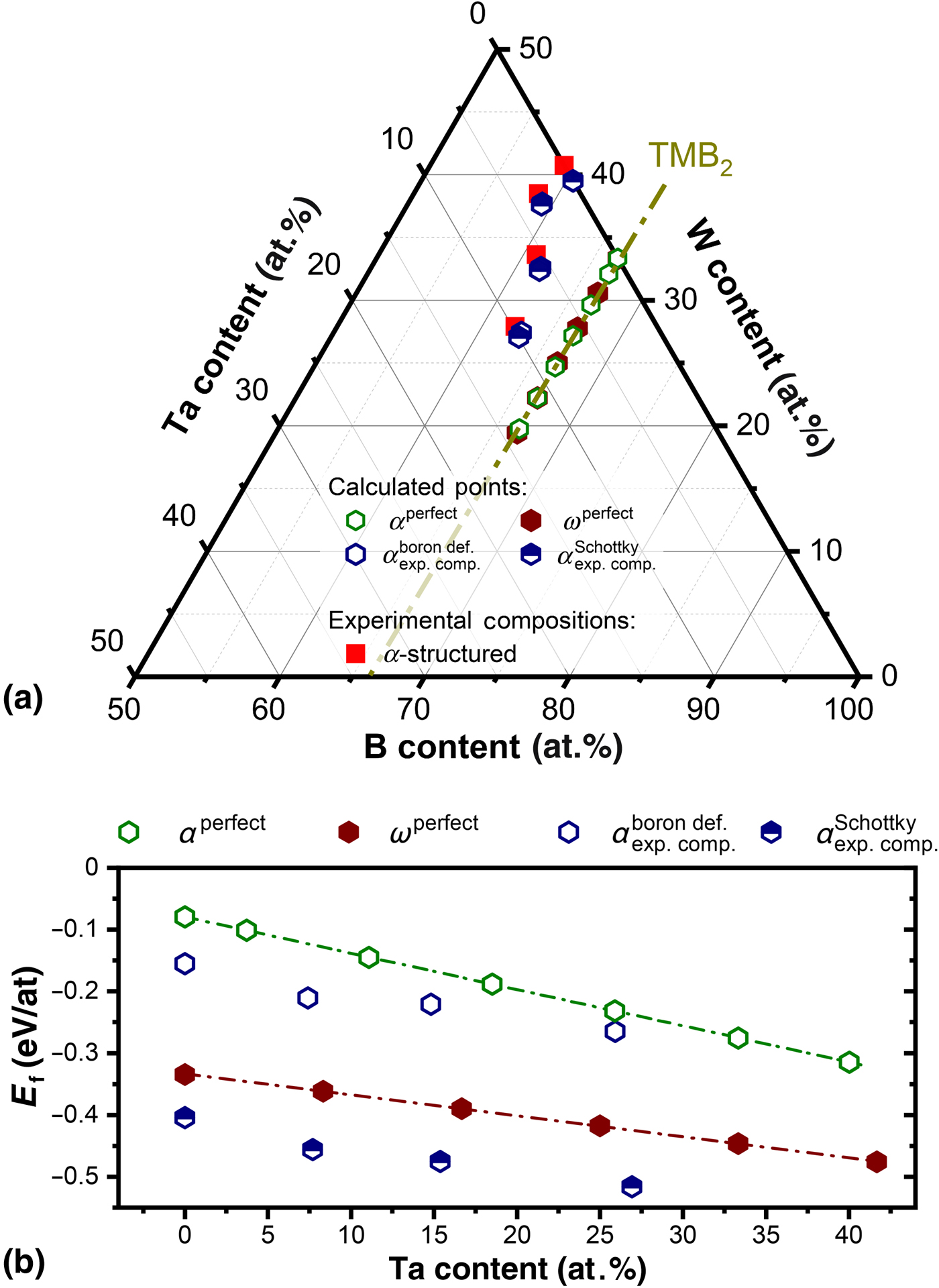
Figure 2(a) shows the B-rich part of the ternary W-Ta-B concentration triangle with indicated experimentally obtained compositions of our coatings [WB1.78 (59.3 at.% B), W0.93Ta0.07B1.76 (58.6 at.% B), W0.86Ta0.14B1.83 (61.1 at.% B), and W0.74Ta0.26B1.87 (62.3 at.% B)]. Furthermore, compositions used for the DFT studies are plotted in Fig. 2(a), whereas open green and filled red hexagons refer to defect-free α- and ω-structures, hence labeled α-perfect and ω-perfect, respectively. In addition, calculated compositions in relation to the experimentally obtained chemical constitutions are labeled with  $\alpha _{{\rm exp}{\rm. \; comp}{\rm.}} ^{{\rm boron\; def}{\rm.}} $, open blue hexagons, as well as
 $\alpha _{{\rm exp}{\rm. \; comp}{\rm.}} ^{{\rm Schottky}} $, indicated by half-filled blue hexagons, for boron-deficient and Schottky-defected α-crystals, respectively. All coatings exhibit a boron deficiency from the quasi-binary TaB2-WB2 tie-line [indicated in Fig. 2(a) with a yellow dash-dotted line]. The offset between experimental composition and those used for the computational studies simply results from the restrictions made by using limited supercell sizes and the SQS approach.
(a) B-rich part of the ternary W-Ta-B concentration triangle with indicated chemical compositions (obtained by TOF-ERDA) of the sputtered W1−xTaxB2−z films (red squared data points) and chemical compositions used for the DFT studies (data points with full hexagons [labeled with ω perfect, for defect-free crystals) and data points with open hexagons (labeled with α perfect, for defect-free crystals and  $\alpha _{{\rm exp}{\rm. \; comp}{\rm.}} ^{{\rm boron\; def}{\rm.}} $, for B-vacant crystals to meet the experimental chemical compositions) and data points with half-filled hexagons (labeled with
 $\alpha _{{\rm exp}{\rm. \; comp}{\rm.}} ^{{\rm Schottky}} $, for B-vacant and Schottky-defected crystals to meet the experimental chemical composition)]. (b) Energy of formation (E f) as a function of the Ta content for defect-free α- and ω-W1−xTaxB2−z lattices as well as for defected α-structures [same labeling of the data points as in (a)].
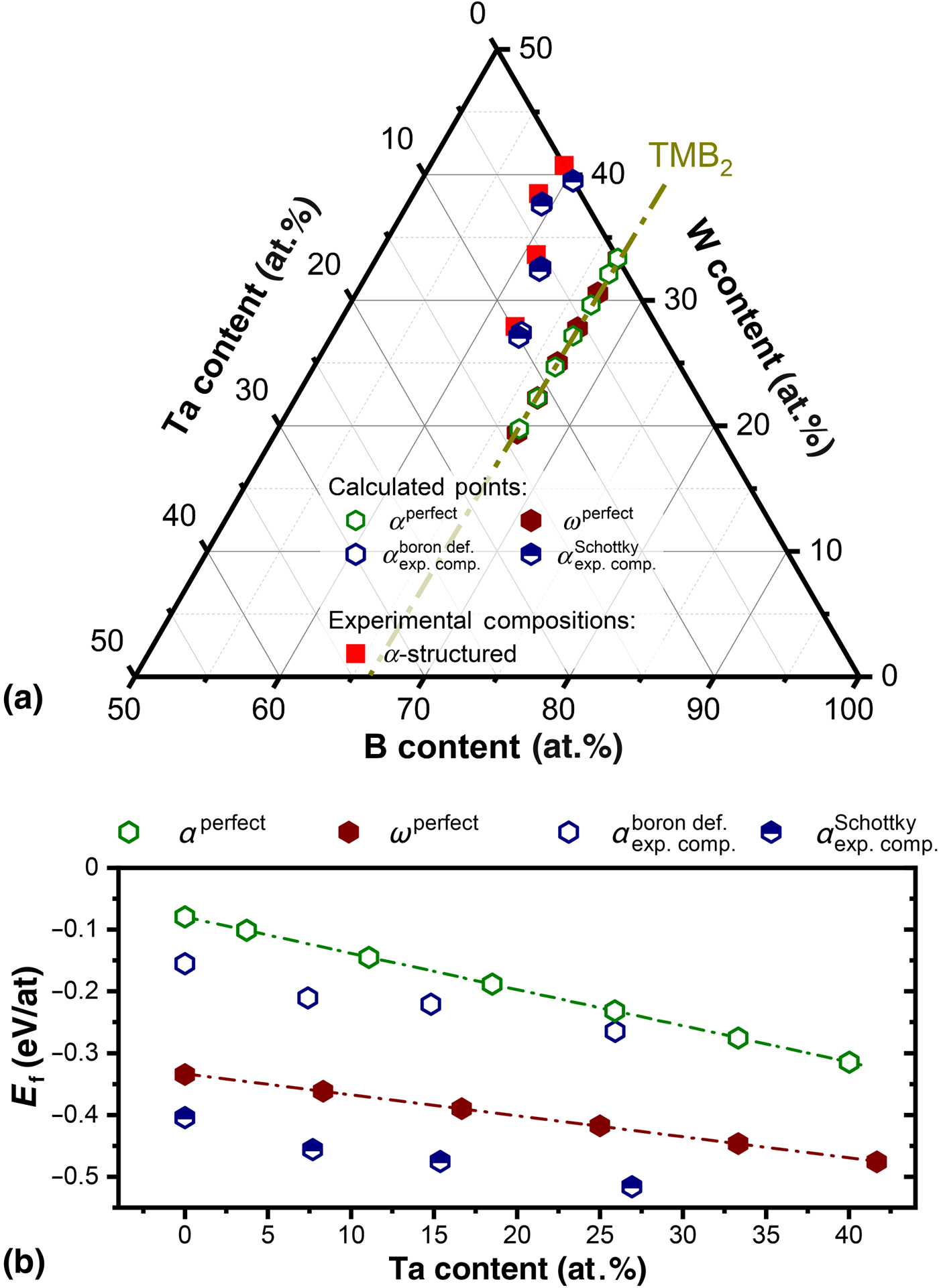
Figure 2(b) shows the results for the energy of formation for defect-free and defected α-W1−xTaxB2−z solid solutions and defect-free ω-W1−xTaxB2−z solid solutions. The data clearly show that considering defect-free structures, the ω-phase (full red hexagons) is always preferred over the α-phase (empty green hexagons). But with increasing Ta content, their difference decreases as far as for TaB2 both structures, α and ω, exhibit nearly the same energy of formation as it is shown in Ref. [Reference Moraes, Fuger, Paneta, Primetzhofer, Polcik, Bolvardi, Arndt, Riedl and Mayrhofer16]. When calculating B-vacant α-structures (to come closer to the experimentally obtained chemical composition), the E f values become more negative with respect to defect-free cells, suggesting the preference for boron vacancies [WB1.78 (9.3 at.% B-vacancies), W0.93Ta0.07B1.76 (11.1 at.% B-vacancies), W0.86Ta0.14B1.83 (7.4 at.% B-vacancies), W0.74Ta0.26B1.87 (5.5 at.% B-vacancies)]. But especially when adding also 3.7% Schottky defects to these B-vacant α-structures (WB1.78 with 3.7 at.% M-vacancies and 13.0 at.% B-vacancies, W0.93Ta0.07B1.76 with 3.7 at.% M-vacancies and 14.8 at.% B-vacancies, W0.86Ta0.14B1.83 with 3.7 at.% M-vacancies and 11.1 at.% B-vacancies and W0.74Ta0.26B1.87 with 3.7 at.% M-vacancies and 9.3 at.% B-vacancies), their E f values are even more negative than those of the ω-structure. We did not consider defected ω-structures, as their energy of formation becomes more positive.[Reference Moraes, Fuger, Paneta, Primetzhofer, Polcik, Bolvardi, Arndt, Riedl and Mayrhofer16] These results clearly proof that for defected materials (having metal and B vacancies), the α-structure is preferred, especially for high Ta contents (decreasing E f and ΔE f between α- and ω-structure with increasing Ta content).
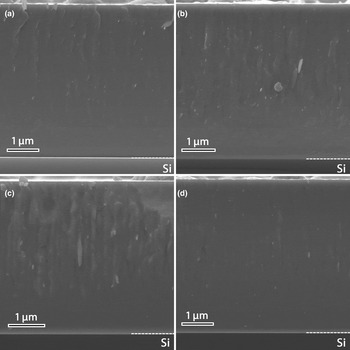
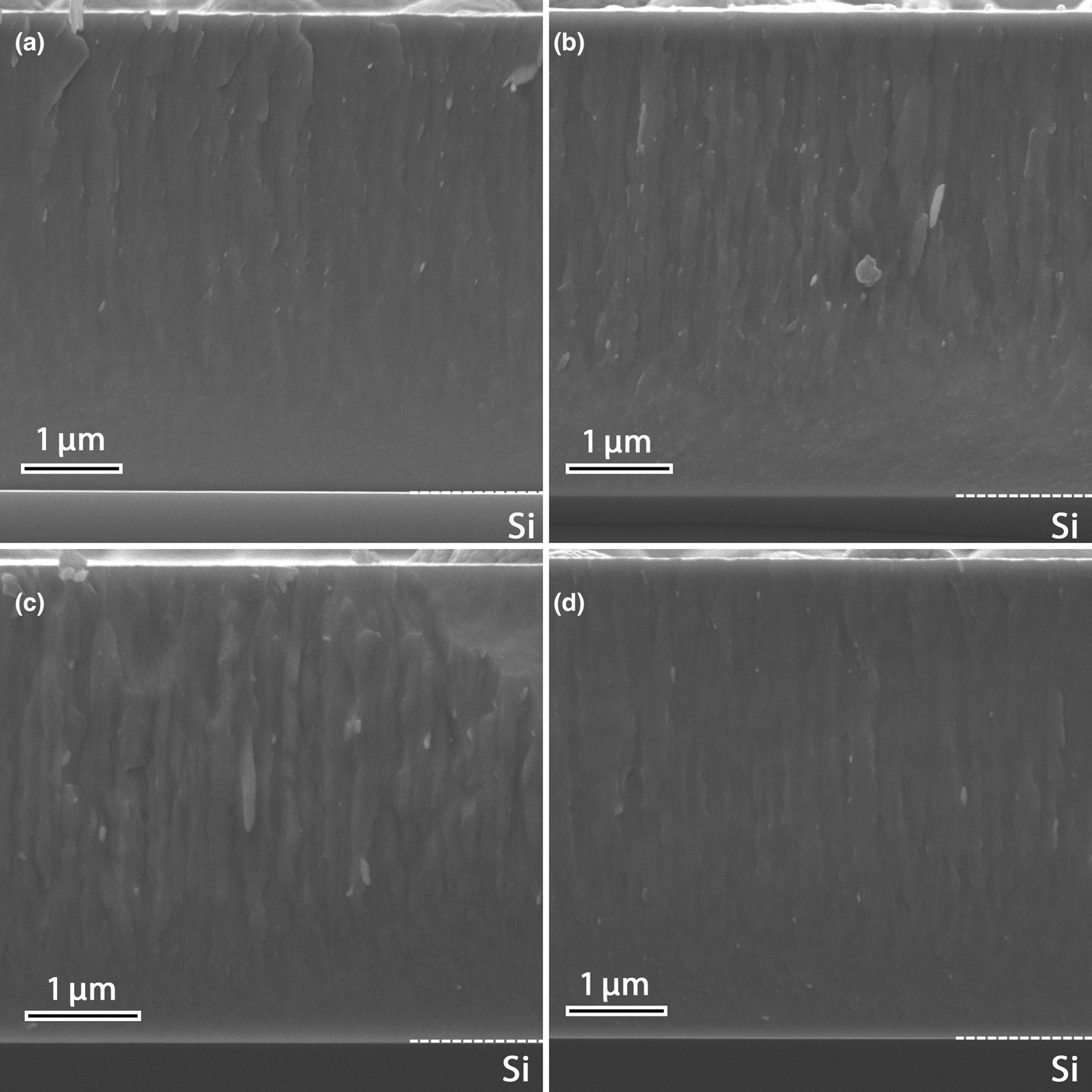
Detailed fracture cross-sectional investigations of our W1−xTaxB2−z thin films (on Si substrates) via SEM (Fig. 3) show a dense, fine (almost featureless) fibrous growth morphology. The coating thickness slightly changes with the Ta content (WB1.78: 4.7 µ m, W0.93Ta0.07B1.76: 4.5 µm, W0.86Ta0.14B1.83: 4.2 µm, W0.74Ta0.26B1.87: 4.5 µm), resulting in a growth rate of 1.2–1.3 nm s −1. The overall impression by the SEM images in combination with the XRD results for these coatings suggests that with increasing Ta content also the columnar crystal diameter decreases.
SEM fracture cross-section of as-deposited (a) WB1.78, (b) W0.93Ta0.07B1.76, (c) W0.86Ta0.14B1.83, and (d) W0.74Ta0.26B1.87 thin films.
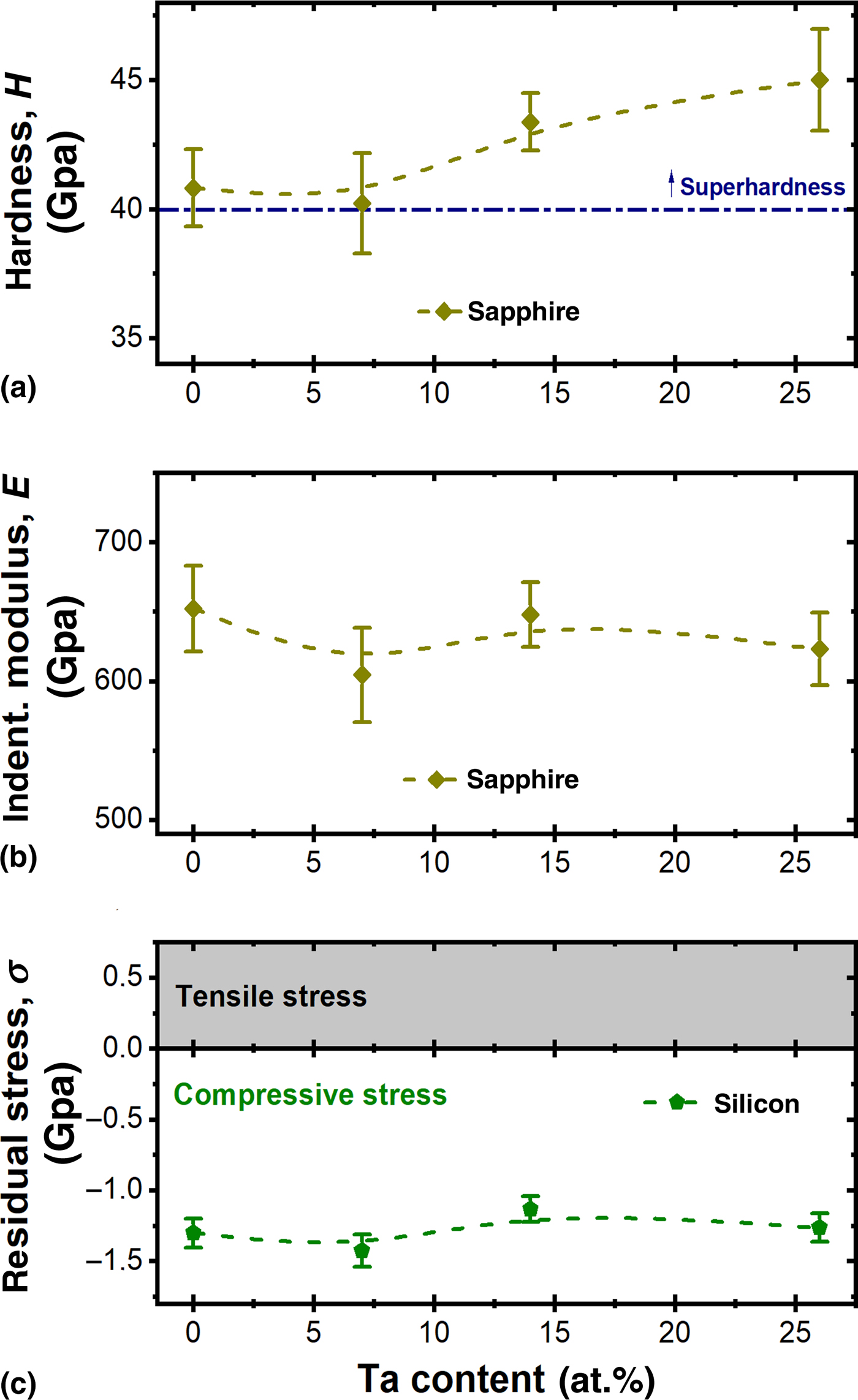
Nanoindentation measurements of our single-phased α-structured WB1.78, W0.93Ta0.07B1.76, W0.86Ta0.14B1.83, and W0.74Ta0.26B1.87 thin films (on sapphire substrates) show hardness values of 40.8 ± 1.5, 40.2 ± 1.9, 43.4 ± 1.1, and 45.0 ± 2.0 GPa [Fig. 4(a)]. While the hardness generally increases with increasing Ta content, the indentation moduli show a slight tendency of decreasing values from 652 ± 30 to 623 ± 26 GPa. As the residual compressive biaxial stresses (obtained by measuring the curvature of coated Si substrates) show no dependence on the Ta content [σ between −1.1 and −1.4 GPa, Fig. 4(c)] and the growth morphology is also rather similar (with comparable column sizes) and the dominating strengthening mechanism can be related to solid solution hardening effects (including parelastic and dielastic contributions as TaB2 and WB2 have different lattice parameters and shear moduli[Reference Moraes, Riedl, Fuger, Polcik, Bolvardi, Holec and Mayrhofer11]).
(a) Hardness (H), (b) indentation moduli (E), and (c) residual stresses (σ) of our single-phased α-W1−xTaxB2−z coatings with x = 0, 7, 14, 26 at.%. The nanoindentation experiments are conducted on coated sapphire samples, whereas the stresses are obtained by curvature measurements of coated Si substrates.
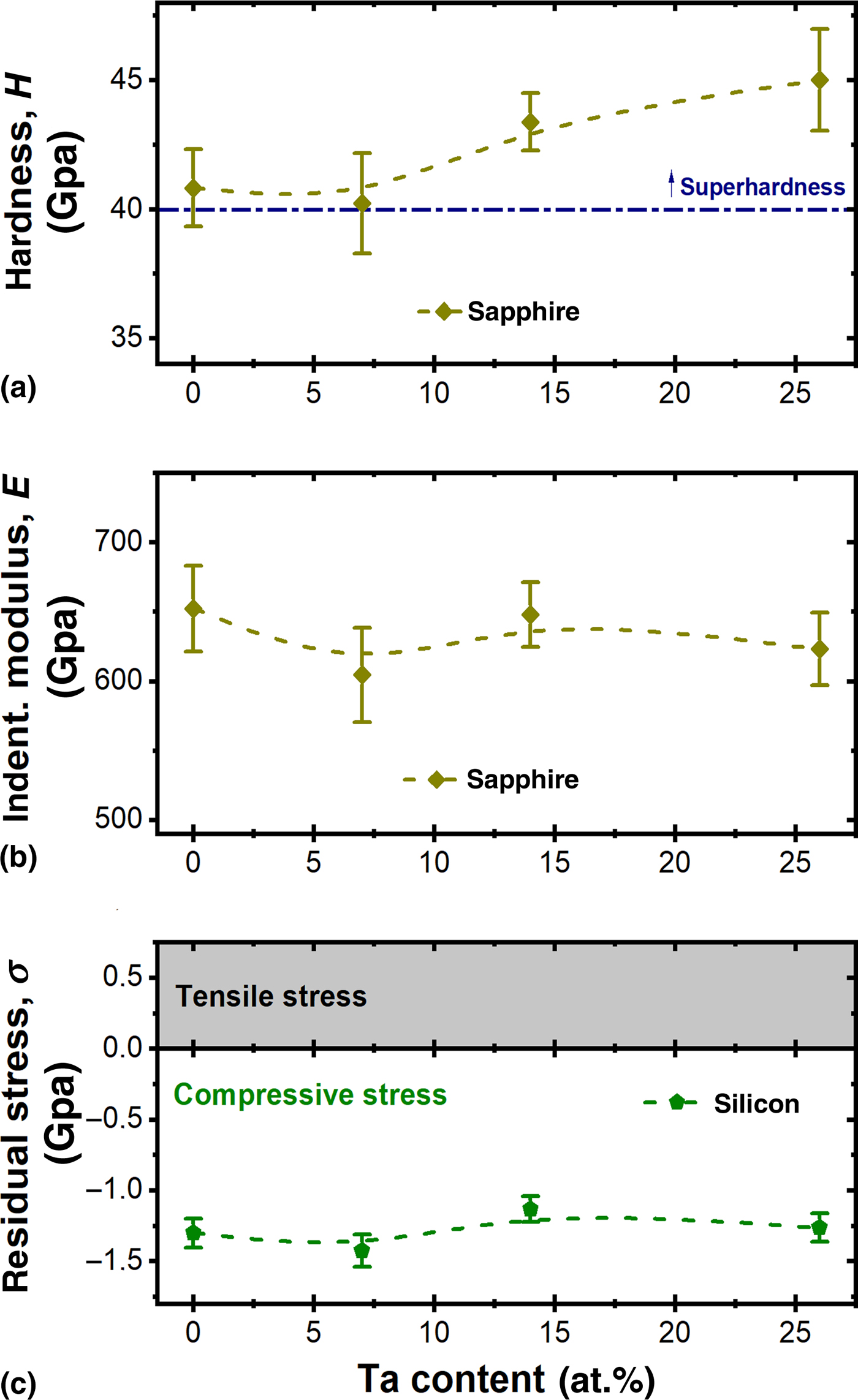
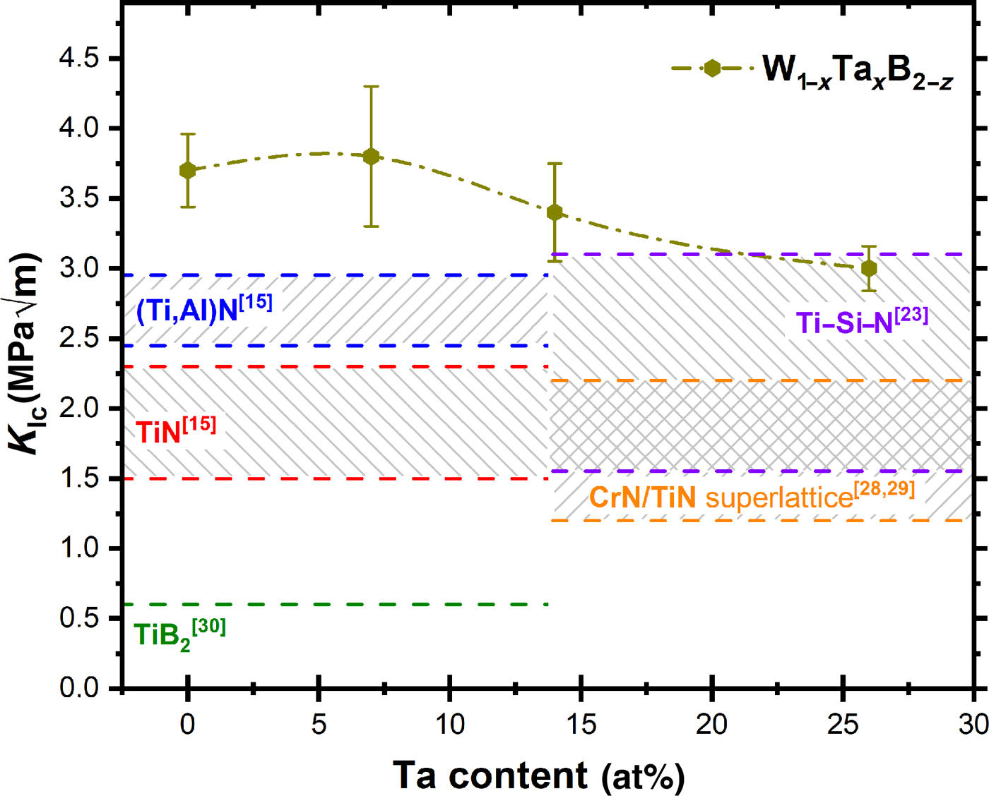
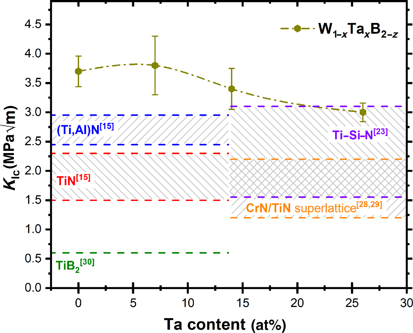
The fracture toughness (obtained by in situ micromechanical bending tests) initially increases from 3.7 ± 0.3 MPa√m (WB1.78) to 3.8 ± 0.5 MPa√m (W0.93Ta0.07B1.76), but then decreases to 3.0 ± 0.2 MPa√m (W0.74Ta0.26B1.87) with the addition of Ta. The W0.93Ta0.07B1.76 coating, which exhibits the highest K IC value (3.8 ± 0.5 MPa√m) among our coatings studied, also exhibits the highest compressive stresses (−1.4 GPa), lowest hardness (40.2 ± 1.9 GPa), and lowest indentation modulus (604 ± 34 GPa). The ratios H/E and H3/E2, which are often used to qualitatively rate materials for their failure resistance, actually increase with increasing Ta content from 0.06 to 0.07 and 0.16 to 0.23, respectively. However, our findings that the fracture toughness of α-W1−xTaxB2−z generally slightly decreases with increasing Ta content excellently fits to DFT calculations showing that α-WB2 has a higher ductility parameter (Cauchy pressure, Pugh and Frantsevic criteria on the Poisson ratio) than α-TaB2.[Reference Moraes, Riedl, Fuger, Polcik, Bolvardi, Holec and Mayrhofer11] The addition of Ta should thus only slightly decrease ductility while it significantly helps to prepare α-structured W1−xTaxB2−z solid solutions. WB2 would actually favor the ω-type structure, while α-TaB2 has almost the energy of formation as ω-TaB2 (when considering vacancies, which are always present in PVD coatings, α-TaB2 is preferred over ω-TaB2[Reference Moraes, Fuger, Paneta, Primetzhofer, Polcik, Bolvardi, Arndt, Riedl and Mayrhofer16]). For comparison, recently published K IC values of sputtered nitrides (which are considered typically as more ductile than diborides)––(Ti,Al)N[Reference Bartosik, Rumeau, Hahn, Zhang and Mayrhofer15], CrN/TiN[Reference Hahn, Bartosik, Arndt, Polcik and Mayrhofer28, Reference Hahn, Bartosik, Soler, Kirchlechner, Dehm and Mayrhofer29], Ti-Si-N[Reference Bartosik, Hahn, Zhang, Ivanov, Arndt, Polcik and Mayrhofer23], and TiN[Reference Bartosik, Rumeau, Hahn, Zhang and Mayrhofer15]––are added to Fig. 5. All of these nitride-based materials, although tested with the same procedure and even the same equipment, clearly exhibit lower fracture toughness values. The reported K IC value of TiB2 thin films, which are often used as a benchmark for TM diborides is ~0.6 MPa√m.[Reference Wang, Shi, Gross, Pureza, de Mesquita Lacerda and Chung30] This again agrees with DFT calculations[Reference Moraes, Riedl, Fuger, Polcik, Bolvardi, Holec and Mayrhofer11] yielding that α-TiB2 exhibits a much more brittle behavior than α-WB2.
Critical stress intensity factor (K IC) values determined by micromechanical bending tests of microscopic cantilevers, produced from the coatings. The tests were carried out with the following samples: WB1.78, W0.93Ta0.07B1.76, W0.86Ta0.14B1.83, and W0.74Ta0.26B1.87. Literature values of (Ti,Al)N, CrN/TiN, Ti-Si-N, TiN, and TiB2 are indicated by the blue, orange, purple, red, and green areas and lines, respectively.
Conclusions
We have successfully deposited single-phase α-structured ternary W1−xTaxB2−z up to a tantalum content of ~26 at.% (at the metal sublattice). For higher Ta contents, an additional phase develops also due to the thereby reduced B content. Therefore, further DFT and experimental investigations concentrated on ternary materials with Ta contents below 30 at.%. The prepared single-phase α-structured coatings, WB1.78 (59.3 at.% B), W0.93Ta0.07B1.76 (58.6 at.% B), W0.86Ta0.14B1.83 (61.1 at.% B), W0.74Ta0.26B1.87 (62.3 at.% B), and TaB1.01 (53.1 at.% B), exhibit hardness values of about 40.8, 40.2, 43.4, and 45.0 GPa, respectively, which generally increase with increasing Ta content due to solid solution hardening effects. Their indentation moduli slightly decrease from 652 to 623 GPa with increasing Ta content, and the residual stresses are with values between −1.1 and −1.4 GPa almost independent from the Ta content (for the compositional range investigated). In agreement with DFT calculations, the fracture toughness decreases from K IC = 3.7 ± 0.3 MPa√m (WB1.78) to 3.0 ± 0.2 MPa√m (W0.74Ta0.26B1.87) with the addition of Ta. The lowest Ta-containing ternary α-W0.93Ta0.07B1.76 coating, which exhibits a −0.1 GPa larger compressive stress than α-WB1.78, exhibits with 3.8 ± 0.5 MPa√m the highest KIC value. The results clearly reveal the enormous potential of α-WB2-based diboride coatings in combining high strength with high fracture toughness, and proof the tremendous added value of DFT, when guiding coating design and investigations.
Acknowledgment
The authors greatly acknowledge the financial support of Plansee Composite Materials GmbH, Oerlikon Balzers Surface Solutions AG and the Christian Doppler Gesellschaft within the framework of the Christian Doppler Laboratory for Application Oriented Coating Development. SEM, TEM, and XRD investigations were carried out using facilities of the XRC and USTEM centers of TU Wien, Austria.