I. INTRODUCTION
In 3G voice/data systems, users may be moving, while simultaneously performing broadband data access or a multimedia streaming session [Reference Steer1]. A radio technology that is expected to interact with a multi-services network should be able to change between different operating bands and adapt its features according to the different available standards and requirements. Most of the research efforts performed during the last years dealt with issues related to the physical layer of the communication stack; however, despite the growing interest in multi-standard operation, less attention has been devoted to the radio-frequency front-end, which therefore remains one of the most challenging parts of a multi-band radio, [Reference McCune2, Reference Abidi3]. One main reason for the delay in effectively implementing multi-standard transceivers can be attributed to the implementation of the RF transmit power amplifier (PA). Today, dedicated, single standard PAs achieve very good power added efficiency (PAE) and thus long battery lifetime. Any reconfigurable PA, needed for the support of different, not always predefined, communication systems, should compete with such dedicated solutions. A conceptual framework to this is provided by the so-called software-defined radio (SDR), i.e. a radio communication system, using software for the reconfiguration of the digital and analog parts in order to perform the modulation and demodulation of radio signals [Reference Abidi3]. In practice, however, due to the difficulty of implementing the fast signal processing implied in the SDR approach, most of the systems on the market, based on more traditional approaches, are still supporting only a very limited number of standards (e.g. 4 GSM frequencies, UMTS and, possibly, Bluetooth). In the near future, further standards will have to be supported, and more could be added during the handset lifetime, hopefully without hardware reconfiguration. One main reason for the delay in effectively implementing multi-standard transceivers can be attributed to the implementation of the RF transmit PA. Today, dedicated, single standard PAs achieve very good PAE and thus long battery lifetime. Any flexible PA, needed for the support of different, not always predefined, communication systems, should compete with such dedicated solutions.
In this paper, we investigate a new PA architecture for effective dual-band operation that would enable the implementation of the above-described scenario, providing a full system level characterization considering as reference test bed a pair of dedicated single-band PAs.
The paper is organized as follows: the description of the dual-band PA architectures under consideration is given in section II, highlighting the advantages and weak points for each topology. In section III, the PA prototypes implemented in the dual-band concurrent architectures are described, while the dual-band PA characterization in CW and with modulated signals is reported and discussed in section IV.
II. DUAL-BAND PA ARCHITECTURES
The main objective of the present paper is the consistent evaluation of two possible architectures of dual-band PA, both suitable for their involvement in concurrent dual-band systems. The first is based on two dedicated PAs combined by a diplexer, while the second is specifically designed to be operated in dual-band state.
A) Combined dedicated PAs
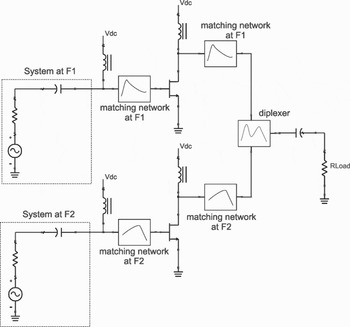
One out of the two dual-band architectures considered in this work is based on the schematic representation reported in Fig. 1. It represents the most straightforward solution that makes use of two dedicated PAs combined by a diplexer. Although for the PA units the designer can access the most mature and advanced design methodologies and technologies, the passive diplexer still represents a very critical part of the entire PA structure. Indeed, this component must guarantee an almost lossless behavior in the transmission paths and an as much as possible isolation. In particular, the former feature is required to preserve the combined efficiency of the entire structure, whereas the latter is required to avoid the cross-modulation between the two dedicated PAs. The constraints on the diplexer become more critical in the case of closer operative spectrum bands. In the two dedicated PAs design, the eventual combination with the diplexer does not require specific additional PA design consideration, only an accurate evaluation of the out-of band termination which might degrade the output power and efficiency of the two units.
Schematic of the concurrent dual-band PA implemented by two combined dedicated PAs.

B) Dual-band single PA
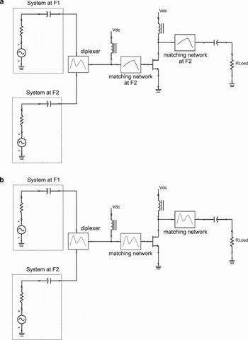
The PA architecture under investigation in this paper is represented by the dual-band single PA, i.e. a circuit designed around a single active device and able to simultaneously operate at two different frequency bands. The schematic of the concurrent PA is reported in Fig. 2, where the dual-tuned matching networks are synthesized by either passive or distributed elements properly dimensioned, without external tuning controls. The basic principle discussed in [Reference Bespalko, Messaoudi and Boumaiza4, Reference Colantonio, Giannini, Giofre and Piazzon5] for the development of a dual-tuned matching network can be effectively considered for the concurrent dual-band PA. In this configuration, the two signal sources are combined prior to being applied to the PA input. The design method of a concurrent dual-band PA based on multi-tuned networks composed of lumped elements is discussed in detail in [Reference Cidronali, Giovannelli, Magrini and Manes6].
Concurrent dual-band PA schematic, implemented by a dual-band PA.

III. PA PROTOTYPES DESIGN
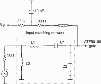
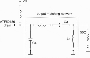
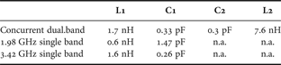
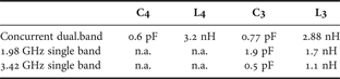
The investigation carried out in this paper relies on prototypes designed and fabricated using low-cost off-the-shelf active devices along with discrete SMD passive components assembled on an FR4 0.8-mm-thick evaluation printed circuit board designed with microstrip technology. The selected active device was ATF50189 from AVAGO Technologies, a medium power enhanced mode p-HEMT with a cutoff frequency of 6 GHz and a 1 dB compression point of 29 dBm at 2 GHz. The optimum bias point for efficiency, linearity, and gain was found to be with a 4.5 V drain supply voltage with a corresponding quiescent current of 200 mA. The chosen bias point drives the ATF50189 transistor in AB class operation. The design was based on load- and source-pull simulations carried out at the two fundamental frequencies of 1.98 and 3.42 GHz, adopting a nonlinear device model that included the package parasitic; simulations provided saturated output powers of 28 and 26 dBm, respectively, in the lower and higher frequency bands with a PAE of approximately 40 and 35% at the 1 dB gain compression point. The implementation of the source and load terminations defined by the source- and load-pull analysis was obtained by using lumped elements matching networks [Reference Cidronali, Giovannelli, Magrini and Manes6]. This technique, by employing a different approach with respect to standard microstrip technology [Reference Bespalko, Messaoudi and Boumaiza4, Reference Colantonio, Giannini, Giofre and Piazzon5], enabled the achievement of highly compact prototypes. All the designed PAs adopt the same general topology for the input and output matching networks, whose schematics are represented in Figs 3 and 4. Different nominal values and the absence of some of the components determine the difference between the prototypes. In addition, the input network accommodates a stabilizing network that has been implemented by all three prototypes. The presence of shunt capacitors at both the gate and drain terminals, C2 and C4 in the figure, provides a short circuit to the second harmonic and an open circuit at the fundamental frequency.
Prototypes input matching network circuit schematic.

Prototypes output matching network circuit schematic.

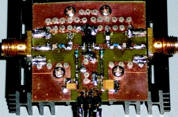
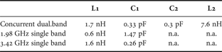
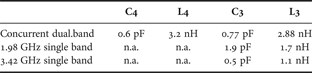
The selected pi-topology exhibits high out-of-band frequency rolloff and is capable of inserting a null in the transfer characteristic between the two fundamental frequency bands at 1.98 and 3.42 GHz, thus enhancing isolation between frequency bands. To properly define the networks, additional conditions for maximum efficiency and 1 dB compression output power under large signal excitations were taken into account. A detailed description of the design approach is given in [Reference Cidronali, Giovannelli, Magrini and Manes6], whereas Tables 1 and 2 report, respectively, the input and output matching network component values. Three PA modules were fabricated using in-house facilities according to the values reported in Tables 1 and 2; a picture of the concurrent dual-band PA prototype is reported in Fig. 5.
Dual-band PA prototype adopted in the measurement implemented in FR4 and SMD components.

Input matching network L–C values.
Output matching network L–C values.
IV. EVALUATION RESULTS
The three PA modules were adopted to implement the two concurrent dual-band PA configurations, namely the combined PAs and the dual-band PA, respectively represented in Figs 1 and 2. The two configurations are tested against small signals, large signals, and digitally modulated signals; the following sub-sections present the experimental results along with a discussion about the performance of the concurrent dual-band PA. The diplexer used in the large-signal test benches is realized in microstrip technology and provides insertion losses of 0.6 and 0.8 dB, respectively, at 1.9 and 3.4 GHz, and isolation between the two channels better than 30 dB and a return loss higher than 20 dB.
A) Small-signal evaluation
The preliminary test was performed in the small-signal regime to assess prototype performance and to verify the consistency of the comparison.
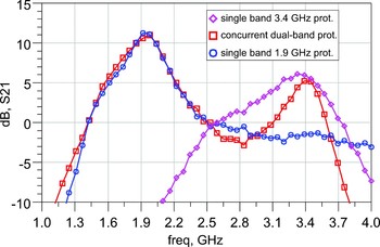
The measured small-signal gains associated with the concurrent dual-band PA and with the two single-band PAs prototypes are compared in Fig. 6. The figure indicates that at 1.98 GHz, the maximum linear gain is approximately 11 dB for both single-band and dual-band circuits. In the 3.4 GHz band, the PA prototypes exhibit a maximum linear gain of 6 dB at 3.42 GHz, and present a 0.5 dB gain bandwidth of approximately 60 MHz. Input and output return losses are not reported but are below −15 dB in the respective frequency bands for all the PAs. Small-signal characterizations have indicated a very close correspondence between the single-band circuits and the concurrent dual-band PA in terms of both input/output return loss and gain. These results show that the design of a concurrent dual-band PA using compact lumped elements is feasible without loss of performance at small signal and makes the characterization and comparison with large and modulated signals meaningful.
Measured small-signal gain for the concurrent dual-band and the two single-band prototypes.

B) Large-signal CW characterization
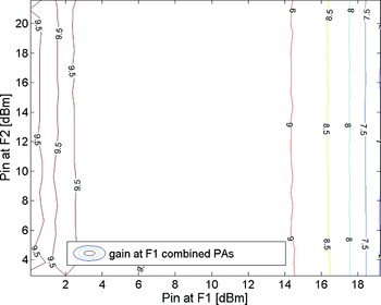
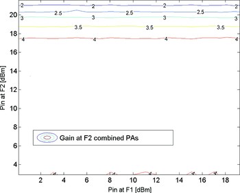
The first set of measurements test bench is deployed to fully characterize PA prototypes with CW large-signal excitations. The data are useful to compare the maximum linear power, gain, and efficiency of the two architectures. In particular, the comparison between power gains as a function of the two CW signals at 1.98 GHz (F1) and 3.4 GHz (F2), reported in Figs 7–10, show that the combined PA architecture is capable of maintaining the two channels mostly separated producing a gain compression that is insensible from the concurrent signal at the side band.
Power gain (dB) in large signal regime evaluated at the frequency of 1.98 GHz as function of input power at 1.98 GHz (F1) and 3.45 GHz (F2), for the combined PAs architecture.

Power gain (dB) in large signal regime evaluated at the frequency of 3.4 GHz as function of input power at 1.98 GHz (F1) and 3.45 GHz (F2), for the combined PAs architecture.

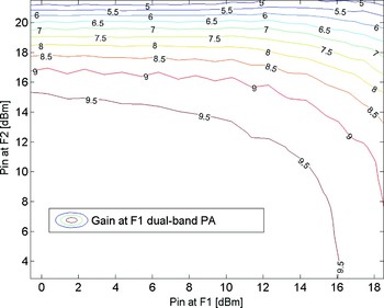
Power gain (dB) in large signal regime evaluated at the frequency of 1.98 GHz as function of input power at 1.98 GHz (F1) and 3.45 GHz (F2), for the dual-band PA architecture.

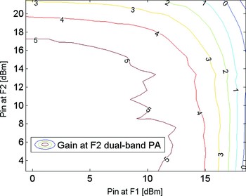
Power gain (dB) in large signal regime evaluated at the frequency of 3.4 GHz as function of input power at 1.98 GHz (F1) and 3.45 GHz (F2), for the dual-band PA architecture.

On the contrary, in the dual-band PA, the mutual interaction between signals at the two frequencies is evidenced by curve constant gain loci. Nevertheless, although the effect of the side band was quite evident, the effect of the output diplexer is such that the maximum output power was slightly higher. For example, we can notice that at 1.98 GHz for input power equal to 16 dBm the gain is 8.7 dB for the combined PAs and 9.5 dB for the dual band. The latter condition is maintained only when the input signal at 3.4 GHz is lower than 10 dBm. Similar behavior is observed with respect to the power gain calculated at 3.4 GHz. From the contour plots in Figs 9 and 10, it is observed that the loci corresponding to 8.5 and 4 dB correspond to the linear gain that the dual-band PA can provide and, consequently, the input ranges that guarantee linear operation of the PA. Differently, in the case of the combined PAs, the linearity in one frequency band does not depend on the side band.
From the contour plots observed in the case of the combined PAs and in the case of the dual-band PA, the presence of the diplexer and the mutual interaction between carriers, determine the output power in correspondence of a power gain 1 dB compression reported in Table 3, from which it is possible to conclude that the two architectures are capable of providing similar output power.
Simultaneous maximum linear output power (at 1 dB gain compression).

A further very significant figure is represented by the PAE. In the case of dual band, concurrent PA is calculated by

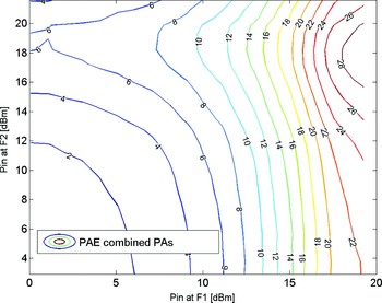
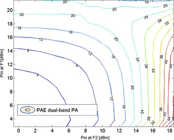
where P dc takes into account the total current drawn by the PA modules. The PAE as a function of the input power at the two carrier frequencies, respectively, for the combined PAs and the dual-band PA architectures, are reported in Figs 11 and 12.
Power added efficiency (%) in large signal regime as function of input power at 1.98 GHz (F1) and 3.45 GHz (F2), for the combined PAs architecture.

Power added efficiency (%) in large signal regime as function of input power at 1.98 GHz (F1) and 3.45 GHz (F2), for the dual-band PA architecture.

Experimental verification confirms the intuition that the dual-band PAE takes advantage of current reuse that is inherent in the use of a single power device, when compared with the case of combined PAs, which need twice the DC power to bias the two PAs. This determines almost a factor of 2 in the PAE for the dual-band PA for almost the entire range of evaluation. In particular at 1 dB gain compression, the PAE achieved with the combined PA architecture is in the range of 20%, as evidenced in Fig. 11, while in the case of the dual-band PA it reaches 32%; see Fig. 12. The maxima are 28 and 44%, respectively, for the combined PAs and the dual-band PA architectures. By this figure, we can observe a significant improvement of the dual-band PA with respect to the combined PA architecture.
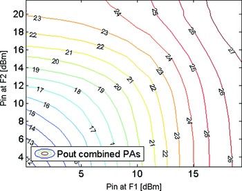
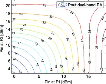
Finally, Figs 13 and 14 report the total output power for the two architectures calculated by summing the power level at the two carrier frequencies. From the contour plots, it is observed that, regardless of linearity concerns, the total power provided by the two systems are slightly the same.
Total output power (dBm) in large signal regime as function of input power at 1.98 GHz (F1) and 3.45 GHz (F2), for the combined PAs architecture.

Total output power (dBm) in large signal regime as function of input power at 1.98 GHz (F1) and 3.45 GHz (F2), for the dual-band PA architecture.

C) Dual-band PA-modulated signal characterization
The next test concerns the capability of the dual-band PA architecture to deal with modulated signals and its performances are compared with the dedicated single-band PAs; henceforth the combined PAs architecture is no longer considered.
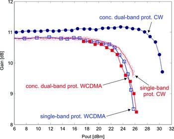
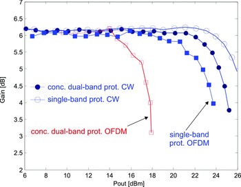
In this case, the base-band signals were downloaded in the arbitrary signal generators (Agilent ESG 4438C) by using the tools available in the Agilent ADS2006A systems. Two different digitally modulated signals were employed to evaluate PA performance: a 3GPP up-link W-CDMA 3.84 MHz chip rate signal at 1.98 GHz and a 5 MHz OFDM 16-QAM signal at 3.42 GHz corresponding to one of the WiMAX modes. The output of the PA under test was connected to the VSA (Agilent N9020, 26 MHz bandwidth), which was synchronized with the two arbitrary signal generators. The first set of data refers to the large signal gain plotted against the output power for the three PA modules; the comparisons between several operating conditions are shown in Figs 15 and 16, for the lower and higher frequency bands, respectively, which also include CW for the sake of better comparison. A discussion about the differences between PA performance is reported in [Reference Cidronali, Giovannelli, Magrini and Manes6].
Gain curve versus output power for CW and WCDMA modulated excitations, both with carrier at 1.98 GHz.

Gain curve versus output power for CW and OFDM modulated excitations, both with carrier at 3.42 GHz.

It is observed that when the amplifiers are driven by a single modulated signal, peak power at 1 dB gain compression point decreases: this effect is explained by the fact that gain compression in PAs driven by digitally modulated signals occurs at lower power levels than for 1-tone CW signals, as described in [Reference Gutierrez, Gard and Steer7]. In addition, load pull CAD analysis and successive design were performed based on a CW test signal, whereas experimental results show that the optimum load impedance for maximum linear output power as well as peak efficiency varies, depending on the characteristics of the input signal, i.e. pulsed, modulated, or CW [Reference Ghanipour, Stapleton and Kim8]. Concurrent mode was then operated by simultaneously feeding the dual-band PA with OFDM and WCDMA signals at the two center band frequencies. Reduction of peak output power with respect to single-channel excitations is mainly due to the simultaneous presence of two modulated signals in the same device, which cause cross-modulation between the two time-varying envelopes. Resulting 4 and 4.5 dB peak power reductions at 1.98 and 3.42 GHz, respectively, were measured with respect to the single-channel cases.
Moving on to system level figures, the 5.6% EVM WiMax standard limit and a minimum ACPR of 33 dBc for a WCDMA signal as settled by the 3GPP specifications have been taken as a reference for power and efficiency values. The goal of the large-signal characterization has been focussed on the evaluation of peak output powers and the resulting PAE levels achievable in the two frequency bands with both concurrent dual-band and single-band excitations so as to satisfy EVM and ACPR constraints.
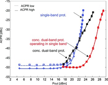
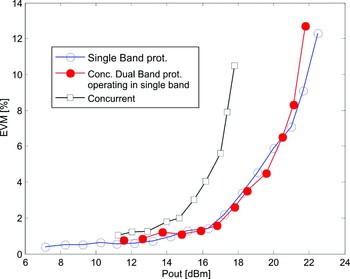
From Fig. 18 it is observed that at 1.98 GHz, the maximum achievable output power, due to ACPR constraints, is 27.5 dBm when the dual-band PA is working in single-channel mode, while for the concurrent dual-band case this limit decreases to 23 dBm. Data in Fig. 17 show EVM versus output power results for single-channel operation and dual-band mode at 3.42 GHz: a maximum output power of 20 dBm is achieved in the first case while when the dual-band PA is working in concurrent mode, maximum output power settles to 17 dBm. The above data indicate that a significant change in performance arises when the PA is driven in the concurrent dual-band mode, specifically resulting in a peak power backoff of about 4.5 and 3 dB, respectively, for the lower and higher frequency bands to meet the EVM and ACPR restrictions. Envelope cross-modulation and inter-modulation explain the EVM and ACPR increased growth with input power when compared with single-channel mode. Experimental data showed that a 2 dB backoff is necessary with concurrent operation to maintain the EVM at 4.1%.
Adjacent channel power ratio measured at 5 MHz offset and integrated over the bandwidth, for the single band and the dual-band prototypes with the WCDMA signal at 1.98 GHz.

Error vector magnitude measured for the single band and the dual-band prototypes with the OFDM signal at 3.42 GHz.

V. CONCLUSION
This paper has dealt with a feasibility study for a concurrent dual-band PA design and characterization for 1.98 GHz 3GPP UL WCDMA and 3.42 GHz 5 MHz 16QAM WiMAX digital systems. The proposed PA was compared with two test beds: the first consisted of a combined PA architecture while the second is based on single-band PAs. The CW characterization demonstrated that in spite of the inherent mutual interaction between carriers, the dual-band PA prototypes provide similar output power at 1 dB gain compression than combined PA architecture. The dual-band PA amplifier exhibited simultaneous peak power levels of 24 and 17 dBm in the lower and higher bands to maintain ACPR and EVM requirements below 33 dBc and 5%, respectively. With respect to a combined PA architecture, the concurrent dual-band PA delivers a 12% higher system efficiency with a 1.5 dB backoff in peak output power. It can be concluded that the proposed solution is capable of providing the same system level performance of more conventional solutions while increasing the overall PAE and allowing a significant reduction of system complexity.
ACKNOWLEDGEMENT
The authors wish to thank Agilent Technology Italy, which provided part of the equipment for system level characterization. The research reported was performed in the context of the network TARGET – “Top Amplifier Research Groups in a European Team” and supported by the Information Society Technologies Programme of the EU under contract IST-1–507893-NOE, www.target-net.org.
 Alessandro Cidronali received the Laurea and Ph.D. degrees in electronics engineering from the University of Florence, Florence, Italy, in 1992 and 1998, respectively. In 1993, he joined the Department of Electronics Engineering, University of Florence, where he became an Assistant Professor in 1999, and where he teaches “Electron Devices” and “Integrated Microwave Circuits”. His research activities cover the study of circuits and system architectures enabling new wideband transmitters, the design of broadband MMICs, and the development of CAD and numerical modeling for microwave devices and circuits. He was Visiting Researcher at the Motorola Physics Science Research Lab from 1999 to 2003 and Guest Researcher at the National Institute of Standards and Technology (NIST), Electromagnetic Division, Non-Linear Device Characterization Group, from 2002 to 2005. In the frame of the EU Network TARGET – “Top Amplifier Research Groups in a European Team”, supported by the information Society Technologies Program, IST-1–507893-NOE, he served as Workpackage Leader for the “Multiband transmitters modeling and design for wireless broadband access” work-packages. He was recipient of the best paper award at the 61th ARFTG Conference. From 2004 to 2006 Dr. Cidronali served as an associate editor for the IEEE Transactions on Microwave Theory and Techniques.
 Iacopo Magrini received the Laurea and Ph.D. degrees in electronics from the University of Florence in 2001 and 2005, respectively. In 2001, he joined the staff of Microelectronic Laboratory (Department of Electronics and Telecommunications) at the University of Florence. In 2002, within the framework of Ph.D. activities, he was at Philips Semiconductor involved in the design of a highly linear front-end for a zero-IF GSM/EDGE receiver. After the Ph.D. he received a grant from the University of Florence as a post-doc and currently he is a lecturer for the courses of High-Frequency Design Lab at the same university. His main research activities include system level simulations along with MMIC design for wireless applications. Starting from 2003, he joined, as a researcher, the NoE-TARGET, whose topic is mainly focused on the development of multi-band multi-standard transceivers for handset applications. Moreover, Dr. Magrini has been involved in several consulting tasks for the development of advanced circuits oriented to industrial and space applications.
 Niccolò Giovannelli received a degree in electronic engineering from the University of Florence in 2007 with a thesis on the dual-band PA design. Afterward he worked, through an MIDRA consortium, in the European network of excellence TARGET, where he was involved in the study of the digital predistortion for an RF power amplifier. Currently, he is working towards a Ph.D. degree at the University of Florence. His research interests are digital baseband predistortion of RF power amplifiers and the study of architectural solutions for the realization of software-defined radios (SDRs).
 Massimiliano Mercanti received the Laurea degree in electronic engineering from Catania University in 2006. He is a Ph.D. student in RF microwave and electromagnetism from Florence University. His doctoral research is on reconfigurable SiGe HBT for high-efficiency RF power amplifiers for wireless applications and optimum matching network for multi-standard RF power amplifiers. He was involved in the development of design and measures of MMIC prototypes within the European network of excellence TARGET.
 Gianfranco Manes became Associate Professor in 1980 and Full Professor in 1985 at the University of Florence, Italy. Dr. Manes contributed, since an early stage, to the field of surface-acoustic-wave (SAW) technology for RADAR signal processing and electronics countermeasure applications. Major contributions were in introducing novel FIR synthesis techniques, fast analogue spectrum analysis configurations, and frequency hopping waveform synthesis. Since the early 1980s, Dr. Manes has been active in the field of microwave modeling and design. In the early 1990s he founded and is currently leading the Microelectronics Lab of the University of Florence, committed to research in the field of microwave devices. In 1982, he was committed to building up a facility for the design and production of SAW and MIC/MMIC devices, as a subsidiary of a Florence’ Radar Company, SMA Spa. In 1984 the facility became a stand-alone, privately owned, microwave company, Micrel SpA, operating in the field of defence electronics and space communications. Present research interest is in the field of microwave systems for wireless applications. Dr. Manes was founder and is presently President of MIDRA, a research consortium between the University of Florence and Motorola Inc. He is member of the Board of Italian Electronics Society and Director of the Italian Ph.D. School in Electronics.