Introduction
The past two decades have seen extensive research aiming to understand the extent to which the electron’s spin degree of freedom can be controlled to add functionality to conventional semiconductor devices.Reference Wolf, Awschalom, Buhrman, Daughton, von Molnar, Roukes, Chtchelkanova and Treger 1 A central effort in this field of “semiconductor spintronics” has been to identify single spin systems that can be measured and manipulated, inspired by the potential use of single spins as elementary units of quantum technologies that perform tasks inaccessible to classical electronics. Indeed, many groundbreaking experiments demonstrated that such single spin control is possible in solid-state systems such as quantum dots, donors in silicon, and defect spins in diamond.Reference Hanson and Awschalom 2 In turn, these demonstrations have led to new challenges: developing applications that benefit from the quantum nature of single spins and engineering large-scale systems in which both single spins and their mutual interactions can be controlled for quantum information processing.
A paramagnetic impurity in diamond known as the nitrogen-vacancy (NV) center has gained increasing attention because its remarkable properties make it a promising candidate for addressing these challenges. The NV center combines long-lived spin coherence, optical spin initialization and measurement, and proximal coupling to individual nuclear spins, enabling the execution of quantum algorithms on coupled spin systems (see the Introductory and Childress and Hanson articles in this issue). Moreover, the ability to perform these operations at room temperature or higherReference Toyli, Christle, Alkauskas, Van de Walle and Awschalom 3 presents the intriguing prospect of utilizing these spins to sense weak electromagnetic fields on nanometer length scales in ambient conditions (see the articles by Hong et al. and Hall et al. in this issue). However, realizing the NV center’s potential requires engineering increasingly sophisticated devices in diamond that integrate technologies from fields such as microwave electronics, photonics, single dopant fabrication, and materials synthesis. We review recent advances in this area, in particular focusing on interfacing NV centers with solid-state electronic devices that enable high-fidelity control over the defect’s quantum degrees of freedom, the controllable fabrication of single defects on technologically relevant length scales, and recently discovered defects in technologically mature materials that enable functionalities beyond those accessible to the diamond NV center.
Interfacing NV centers with solid-state electronics
A primary motivation for pursuing quantum technologies based on solid-state platforms is their inherent flexibility with regard to engineering scalable device geometries. Photolithographic patterning of metal electrodes on diamond surfaces has enabled high-speed quantum control of single NV center spins via the integration of proximal electrical and magnetic control lines. The high dielectric strength and low electrical conductivity of high-purity synthetic diamond permit the application of very large electric fields in micron-scale devices with negligible leakage currents, and diamond’s chemical inertness and high thermal conductivity alleviate problems with heating from the application of large currents to on-chip wires. In this section, we outline a few recent examples of microfabricated devices used to achieve a high degree of control over single NV center spins.
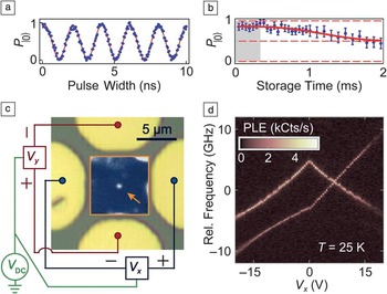
The prototypical example of coherent control of a two level quantum system (a quantum bit, or qubit) is the driving of Rabi oscillations—cyclic transitions between the qubit’s energy eigenstates—through the application of an oscillating field resonant with the energy level spacing. Rabi driving of single NV center spins using resonant AC magnetic fields was first demonstrated nearly a decade agoReference Jelezko, Gaebel, Popa, Domhan, Gruber and Wrachtrup 4 and is now a standard component of NV center spin control. By fabricating a microwave waveguide on the surface of a diamond sample containing NV centers, strong microwave magnetic fields (up to ∼500 G) can be generated locally within the diamond, leading to very fast spin rotations. Figure 1 a shows Rabi oscillations at 500 MHz measured in such a device,Reference Fuchs, Dobrovitski, Toyli, Heremans and Awschalom 5 with a corresponding spin flip time (π rotation) of only 1 ns. With NV center coherence times (T 2) exceeding 1 ms in high-purity synthetic diamond,Reference Balasubramanian, Neumann, Twitchen, Markham, Kolesov, Mizuochi, Isoya, Achard, Beck, Tissler, Jacques, Hemmer, Jelezko and Wrachtrup 6 this allows >106 qubit operations per coherence time. Strong microwave driving fields from on-chip waveguides have also facilitated studies of coherent dynamics of the NV center’s short-lived optically excited state,Reference Fuchs, Dobrovitski, Toyli, Heremans, Weis, Schenkel and Awschalom 7 , Reference Fuchs, Falk, Dobrovitski and Awschalom 8 requiring operations faster than its ∼10 ns lifetime.
(a) Coherent spin rotations of a single nitrogen-vacancy (NV) center in diamond. The nanosecond rotations are achieved by generating intense, resonant magnetic fields using an on-chip coplanar waveguide. P |0〉 represents the population of the electronic spin in its m s = 0 sublevel. (b) Hahn echo measurement of a single nitrogen nuclear spin demonstrating storage and retrieval of quantum information over a timescale of 1.3 ± 0.4 ms. The shaded gray region represents the information storage timescale (T 2 = 350 ± 90 μs) for an analogous measurement performed on the electronic spin. Adapted with permission from Reference Reference Fuchs, Burkard, Klimov and Awschalom10. (c) Optical micrograph of a device used to tune NV center zero-phonon-line optical transitions via the DC Stark effect. Electrical connections to the four metal gates are indicated, and a single NV center 7 μm below the diamond surface is marked by an arrow in the spatial photoluminescence image (inset). (d) DC Stark tuning diagram for the NV center marked in (c), showing the m s = 0 optical transition frequencies (vertical axis) as a function of the symmetric bias Vx (horizontal axis). At Vx ∼ 7 V, the electric field compensates the local strain to restore the orbital degeneracy of an ideal unstrained crystal. Both (c) and (d) are adapted with permission from Reference Reference Bassett, Heremans, Yale, Buckley and Awschalom13.

In addition to the electronic spin, the nitrogen atom intrinsic to each NV center also provides a single, coupled nuclear spin. Due to their smaller magnetic moment, nuclear spins interact only weakly with their fluctuating magnetic environment and therefore have much longer coherence times than their electronic counterparts, suggesting their use as memory nodes in future quantum computing devices. The long spin coherence of nuclei comes with a cost, however, since their weak interaction with magnetic fields makes direct nuclear driving correspondingly slow. Nuclear spin rotations typically require a few microseconds to complete, often exceeding the electronic spin’s inhomogeneous dephasing time (T 2*), thus degrading the fidelity of joint quantum operations between the electronic and nuclear spins. One approach to this problem is the recent development of synchronized pulse sequences on both the electronic and nuclear spins that decouple the electronic spin from its environment during joint operations, removing the constraint set by T 2*.Reference van der Sar, Wang, Blok, Bernien, Taminiau, Toyli, Lidar, Awschalom, Hanson and Dobrovitski 9 Another solution is to use the hybridization between the electronic and nuclear spin states that occurs at the level anticrossing between the ground-state spin sublevels due to hyperfine coupling. Using two on-chip wires, a fast modulation to the vector magnetic field can be engineered to controllably traverse the level anticrossing such that the information stored in the electronic spin is coherently transferred to the nuclear spin and vice versa. This operation can be accomplished in only ∼100 ns, with coherent nuclear storage giving a fourfold improvement over the electronic spin’s T 2 (Figure 1b).Reference Fuchs, Burkard, Klimov and Awschalom 10
To realize the potential of large-scale quantum information processing in diamond, a method is needed to generate controlled entanglement between individually addressable spins. The atom-like nature of the NV center immediately suggests using photons as mediators of quantum information between distant NV centers through coherent optical interactions. Such coherent spin-light interactions have been demonstrated for the NV center, although they require lower-temperature operation (∼10 K) since phonons lead to rapid decoherence of the excited-state orbitals at elevated temperatures.Reference Fu, Santori, Barclay, Rogers, Manson and Beausoleil 11 When orbital coherence approaches the ∼13 ns excited-state lifetime, the fine structure of the direct, or zero-phonon line (ZPL), optical transitions can be used to coherently couple NV center spins with light. For example, dispersive interactions due to laser light close to resonance with the ZPL transitions enable both nondestructive optical measurements of the spin state and controlled optical spin rotations.Reference Buckley, Fuchs, Bassett and Awschalom 12
The ZPL transitions for different NV centers within the same diamond sample are not identical, due to local electrostatic and structural variations within the crystal. The width of the inhomogeneous distribution depends on the sample purity, with center-to-center transition frequency variations of ∼10 GHz even in the purest samples. This poses a major challenge for distributed photonic coupling, which requires photons from separate centers to be indistinguishable within the ∼10 MHz homogeneous line width. Luckily, the transition energies can be precisely tuned by an electric field through the DC Stark effect. By applying voltages to metal surface gates in a device like that shown in Figure 1c, the appropriate electric field can be generated to compensate the intrinsic crystal strain and bring multiple NV centers to optical indistinguishability.Reference Bassett, Heremans, Yale, Buckley and Awschalom 13 – Reference Sipahigil, Goldman, Togan, Chu, Markham, Twitchen, Zibrov, Kubanek and Lukin 15 The electrostatics of such devices are complicated by nonlinear charging effects induced by photoionized donors in the bulk diamond, but these effects can actually be used to enhance their functionality.Reference Bassett, Heremans, Yale, Buckley and Awschalom 13 Figure 1d shows the optical transition frequencies from the ground state to the excited state orbitals as a function of bias, Vx . At Vx ∼ 7 V, the orbital degeneracy of an unstrained crystal is restored, at which point special optical selection rules allow for spontaneous generation of spin-photon entanglement through optical relaxation.Reference Togan, Chu, Trifonov, Jiang, Maze, Childress, Dutt, Sorenson, Hemmer, Zibrov and Lukin 16 By tuning multiple NV centers to optical indistinguishability in this way, two-photon interference effectsReference Bernien, Childress, Robledo, Markham, Twitchen and Hanson 14 , Reference Sipahigil, Goldman, Togan, Chu, Markham, Twitchen, Zibrov, Kubanek and Lukin 15 could lead to the remote entanglement of spatially separated spins in diamond.
Single spins by design
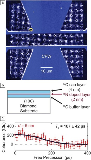
One of the foremost challenges to realizing NV center technologies that couple the spin to external degrees of freedom has been to develop techniques to controllably place single defects with nanometer-scale precision within an otherwise pure diamond substrate. For example, the sensing of external spins using NV center magnetometers is enabled by decreasing the target-sensor distance to tens of nanometers or less (see the article by Hong et al.), and creating long-distance NV center networks using photonic devices requires incorporating individual spins within an optical cavity’s nanoscale mode volume.Reference Aharonovich, Greentree and Prawer 17 The most common approach to address this challenge has been to create “artificial” NV centers in diamond using ion implantation. In this approach, low energy (typically <100 keV) nitrogen ions are impacted into the diamond crystal to place both nitrogen atoms and vacancies, created through ion-lattice collisions, near the diamond surface. Annealing above 700°C induces vacancy diffusion to produce NV centers with a nitrogen to NV center conversion efficiency of a few percent.Reference Rabeau, Reichart, Tamanyan, Jamieson, Prawer, Jelezko, Gaebel, Popa, Domhan and Wrachtrup 18 Since the first demonstrations of single defect fabrication,Reference Rabeau, Reichart, Tamanyan, Jamieson, Prawer, Jelezko, Gaebel, Popa, Domhan and Wrachtrup 18 , Reference Meijer, Burchard, Domhan, Wittmann, Gaebel, Popa, Jelezko and Wrachtrup 19 considerable effort has been devoted to implanting NV centers with spatial accuracies relevant to the aforementioned quantum technologies. A number of complementary techniques have been investigated, including implanting through apertures in scanning probe tips,Reference Weis, Schuh, Batra, Persaud, Rangelow, Bokor, Lo, Cabrini, Sideras-Haddad, Fuchs, Hanson, Awschalom and Schenkel 20 , Reference Pezzagna, Wildanger, Mazarov, Wieck, Sarov, Rangelow, Naydenov, Jelezko, Hell and Meijer 21 patterning implantation with nano-apertures in electron-beam lithography resist,Reference Toyli, Weis, Fuchs, Schenkel and Awschalom 22 and etching nano-posts in implanted diamond substrates.Reference Hausmann, Babinec, Choy, Hodges, Hong, Bulu, Yacoby, Lukin and Loncar 23 The latter two approaches have used widely available methods to fabricate chip-scale arrays of spatially localized single spins with spatial resolutions on the order of 10 nm ( Figure 2 a). Although these implanted NV centers often exhibit widely dispersed and sometimes degraded properties compared with naturally occurring NV centers,Reference Naydenov, Reinhard, Lammle, Richter, Kalish, D’Haenens-Johansson, Newton, Jelezko and Wrachtrup 24 they have proven to be an essential resource in nanostructures such as scanning probe magnetometers,Reference Maletinsky, Hong, Grinolds, Hausmann, Lukin, Walsworth, Loncar and Yacoby 25 and there are ongoing efforts to optimize their properties through advanced annealingReference Naydenov, Reinhard, Lammle, Richter, Kalish, D’Haenens-Johansson, Newton, Jelezko and Wrachtrup 24 and surface preparation techniques.Reference Staudacher, Ziem, Haussler, Stohr, Steinert, Reinhard, Scharpf, Denisenko and Wrachtrup 26
(a) Spatial photoluminescence image of a nitrogen-vacancy (NV) center array fabricated by nitrogen implantation through nano-apertures in electron beam lithography resist and subsequent annealing. The white dots in the image result from NV center photoluminescence; a representative single NV center is circled. A lithographic, short-terminated coplanar waveguide used for electron spin resonance measurements is also visible on top of the implanted spin array (solid light blue color, labeled as CPW in the image). Adapted with permission from Reference Reference Toyli, Weis, Fuchs, Schenkel and Awschalom22. © 2010 American Chemical Society. (b) Illustration showing the growth profile of a nitrogen delta-doped diamond in which NV centers are produced in thin layers (<2 nm) grown by chemical vapor deposition near the diamond surface. (c) Hahn-echo measurement showing the long spin coherence (T 2) of a doped NV center 5 nm from the diamond surface. Both (b) and (c) are adapted with permission from Reference Reference Ohno, Heremans, Bassett, Myers, Toyli, Bleszynski Jayich, Palmstrom and Awschalom27.

Another recently explored approach to spatially localize NV centers is to incorporate nitrogen during epitaxial diamond growthReference Ohno, Heremans, Bassett, Myers, Toyli, Bleszynski Jayich, Palmstrom and Awschalom 27 , Reference Ishikawa, Fu, Santori, Acosta, Beausoleil, Watanabe, Shikata and Itoh 28 (Figure 2b). These efforts aim to capture the exceptional properties of NV centers in isotopically engineered diamond grown by chemical vapor deposition (CVD),Reference Balasubramanian, Neumann, Twitchen, Markham, Kolesov, Mizuochi, Isoya, Achard, Beck, Tissler, Jacques, Hemmer, Jelezko and Wrachtrup 6 with a depth localization defined by the grown-layer thickness. Combined with post-growth electron irradiation and annealing to enhance their creation efficiency, this approach has produced “doped” NV centers in 2-nm-thick layers within 5 nm of the diamond surface.Reference Ohno, Heremans, Bassett, Myers, Toyli, Bleszynski Jayich, Palmstrom and Awschalom 27 Encouragingly, these shallow spins consistently exhibit T 2 of ∼100 μs (Figure 2c). Deeper spins show even longer T 2, reaching nearly 700 μs at 50 nm below the surface. Calculations suggest that such doped NV centers provide sufficient magnetic sensitivity to detect the magnetic dipole moment of a single electron within 15 nm of the diamond surface in only one second, suggesting an exciting future for nanoscale sensing at the single-spin level using engineered materials.
Beyond the NV center
The diamond NV center’s remarkable properties are, in large part, due to the unique material properties of its solid-state host. Diamond’s wide bandgap, low spin orbit coupling, and the ability to remove background nuclear spins through 12C isotopic purification all contribute to the long coherence and photostability of NV centers that enable applications such as those discussed previously. Despite recent progress, however, challenges persist in the production of wafer-scale diamond films, heteroepitaxial layers, and n-type bulk diamond. These limitations have motivated the search for other material systems that exhibit characteristics similar to the NV center but are more amenable to heteroepitaxy and wafer-scale microfabrication.
Following a systematic search based on specific criteria developed to generalize the NV center’s features and associated theoretical modeling, the divacancy in 4H silicon carbide (a hexagonal form of SiC) was identified as an initial candidate as an optically addressable ground-state spin.Reference Weber, Koehl, Varley, Janotti, Buckley, Van de Walle and Awschalom 29 , Reference Gali 30 Unlike diamond, SiC crystals can be grown in a variety of different polytypes, each with a different symmetry and bandgap, which can be combined to form layered heterostructures.Reference Lu, Chandrashekhar, Parks, Ralph and Spencer 31 The most common SiC polytypes are of two hexagonal forms (4H and 6H) and one cubic form (3C), all of which are commercially available in inch-scale wafers.Reference Saddow and Agarwal 32 Each polytype can be controllably doped as either n-type or p-type. Well-developed microfabrication protocols for SiC have already been utilized to produce a variety of electronic,Reference Zetterling 33 optoelectronic,Reference Zetterling 33 , Reference Cheung 34 and electromechanical systems,Reference Zetterling 33 including complementary metal-oxide-semiconductor devices.Reference Ryu, Kornegay, Cooper and Melloch 35 SiC has even been used extensively as a substrate for other technologically relevant materials such as gallium nitride and graphene.Reference Liu and Edgar 36 , Reference Berger, Song, Li, Wu, Brown, Naud, Mayou, Li, Haas, Marchenkov, Conrad, First and de Heer 37
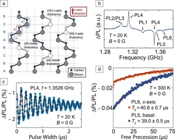
Recent experiments have demonstrated that the divacancy in 4H SiC is indeed a viable defect qubit, sharing many properties with the diamond NV center.Reference Son, Umeda, Isoya, Gall, Bockstedte, Magnusson, Ellison, Morishita, Ohshima, Itoh and Janzen 38 , Reference Koehl, Buckley, Heremans, Calusine and Awschalom 39 The binary crystal nature of SiC leads to a rich structure even for a single defect class such as the divacancy; in 4H SiC, the four distinct divacancy configurations ( Figure 3 a) have unique magnetic resonance spectra, each of which can be detected optically (Figure 3b). Using time-resolved optical and microwave manipulation techniques similar to those used with NV centers, ground-state spin dynamics have been observed, exhibiting spin coherence properties akin to ensembles of NV center spins at comparable temperatures (Figure 3c). Additionally, two previously unobserved and so far unidentified defect states in 4H SiC possess spin characteristics similar to the divacancy’s with spin coherence persisting up to room temperature (Figure 3d). By jointly utilizing the NV-like properties of these defects and the added device potential of silicon carbide materials, the goal of coupling single spins through the host material’s electronic, optical, or mechanical degrees of freedom to create wafer-scale arrays of interacting quantum systems could be within reach.
Spin coherence in SiC defects. (a) Illustration showing the four inequivalent divacancy lattice sites in 4H silicon carbide. (b) Optically detected magnetic resonance spectrum of 4H silicon carbide showing the change in photoluminescence (PL) as a function of magnetic field frequency. Features associated with the four divacancy lattice sites (PL1–4) and two unknown defects (PL5 and PL6) are noted. (c) Demonstration of coherent control (Rabi oscillations) of an ensemble of basal divacancy spins. (d) Room temperature Hahn echo decays from an ensemble of unidentified defects showing spin coherence times of ∼40 μs. Reprinted with permission from Reference Reference Koehl, Buckley, Heremans, Calusine and Awschalom39. © 2011 Nature Publishing Group.

Acknowledgments
We acknowledge financial support from AFOSR, ARO, and DARPA.