Introduction
Advanced communication systems demand multi-band devices to provide various services at different frequencies. Therefore, compact multi-band filters have gained more attention in recent days to enable the optimum usage of space. One of the promising technologies to design sophisticated bandpass filters (BPFs) is substrate integrated waveguide (SIW) technology due to its merits of low-cost, low Q-factor, easy to integrate, and high-power-handling capability [Reference Ding and Wu1]. Mainly, there are three different category topologies have been studied and realized for multi-passband responses in the literature:
(1) BPFs are independently synthesized and then cascaded to accomplish the required multi-passband characteristics based on numerical optimization [Reference Wu, Mao, Yin and Guo2–Reference Dhwaj, Li, Shen and Qin5]. However, the circuit occupies more space.
(2) The wide passband can be divided into sub passbands by inserting multiple transmission zeros (TZs) to realize multi-band BPFs [Reference Quendo, Rius and Person6–Reference Chen, Wu and Li8], namely, so-called coupling matrix synthesis technique. Mainly, this technique is implemented by cascading bandstop with wide BPFs. The limitations are closely separated passbands and large circuit size.
(3) The components such as antennas, filters, and duplexers design using the microstrip multi-mode resonators (MMRs) is a compact design technique because it reduces the number of required resonators. MMRs have been used widely to design compact single- or dual- or triple-band BPFs [Reference Kuo, Yeh and Yeh9–Reference Li, Tang and Xiao12]. Moreover, different SIW dual-mode cavities have also been used for single- and dual-band BPFs [Reference Ren, Hong and Wu13–Reference Zhou, Zhou and Wu17]. The triple-band filter design process with SIW planar technology was discussed in [Reference Dong, Wu and Itoh18–Reference Guo, Zhu and Wu22].
We know that half-mode substrate integrated waveguide (HMSIW) is half of the size in SIW, maintain the same propagation characteristics and field distribution. Therefore, the filter design with HMSIW resonators is compact than SIW resonators [Reference Lai, Fumeaux, Hong and Vahldieck23]. The dual- and triple-band HMSIW filters are designed using a coupling matrix synthesis technique [Reference Sekar and Entesari24, Reference Shakib, Sekar and Entesari25]. But the circuits have closely separated passbands and occupied more space. The HMSIW cavity supports the modes which satisfy the magnetic wall condition. Hence, a wide separated dual- or triple-band BPFs can be made with HMSIW MMRs. In the literature, HMSIW MMRs have not been used in triple-band BPFs to the best of the author's knowledge.
In this paper, HMSIW MMR has been used the first time to design a triple-band BPF. The first four modes of the HMSIW cavity with a slot line have been used to generate two passband responses. Besides, the half-mode defected ground structure (DGS) unit-cell has been loaded into the HMSIW cavity to give the third passband. Therefore, the proposed configuration is compact, and the passbands are broadly separated. This paper is organized as follows. Section “Filter synthesis” outlines the proposed filter synthesis including HMSIW cavity, the analysis of half-mode DGS unit-cell, the impact of slot line perturbation, individual passband tunability, and a notch band design. Section “Fabrication and measurement” presents the fabrication and measured results. Finally, Section “Conclusion” comes to concise conclusions.
Filter synthesis
HMSIW cavity
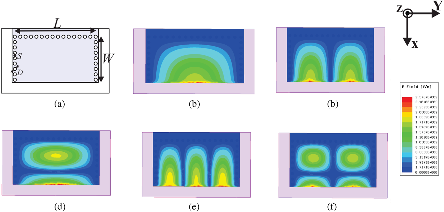
HMSIW cavity is extracted by cutting the SIW cavity along a factitious magnetic wall, as shown in Fig. 1(a). The resonant frequency of TM m−0.5,n,0 of HMSIW cavity is given by

where c is the speed of light, W and L are the dimensions of the cavity, and ɛr and μr are dielectric substrate parameters.
(a) HMSIW cavity. The E-field distribution of first five modes of the cavity: (b) TM 110, (c) TM 120, (d) TM 310, (e) TM 130, and (f) TM 320 (W = 8.5 mm, L = 15.0 mm, S = 1.0 mm, and D=0.6 mm).

The first step is to determine the dimensions of the HMSIW cavity. The initial size of the HMSIW cavity could be calculated with prescribed resonant frequencies of TM 110 and TM 310 modes by the following equation, according to [Reference Guo, Zhu and Wu22]:

The HMSIW cavity is made using an RT/duroid 5880 substrate (0.508 mm thickness) with ɛr = 2.2 and tanδ = 0.0009. The parameters are (in mm): diameter of vias D = 0.6, pitch S =1.0, L = 15, and W = 8.5. According to the synthesized design parameters, TM 110 and TM 310 modes of cavity are expected to be located at 8.6 and 18.3 GHz. This structure is simulated with a high-frequency structure simulator (HFSS) eigenmode simulator, and the electric field distribution of the first five modes of HMSIW cavity is shown in Figs 1(b)–1(f). The first five modes are TM 110, TM 120, TM 310, TM 130, and TM 320, their resonant frequencies are 8.6, 13.6, 18.3, 19.3, and 21.16 GHz. The unloaded quality factor (Q u) of all the modes is above 400.
HMSIW cavity with back-to-back connected DGS unit-cell
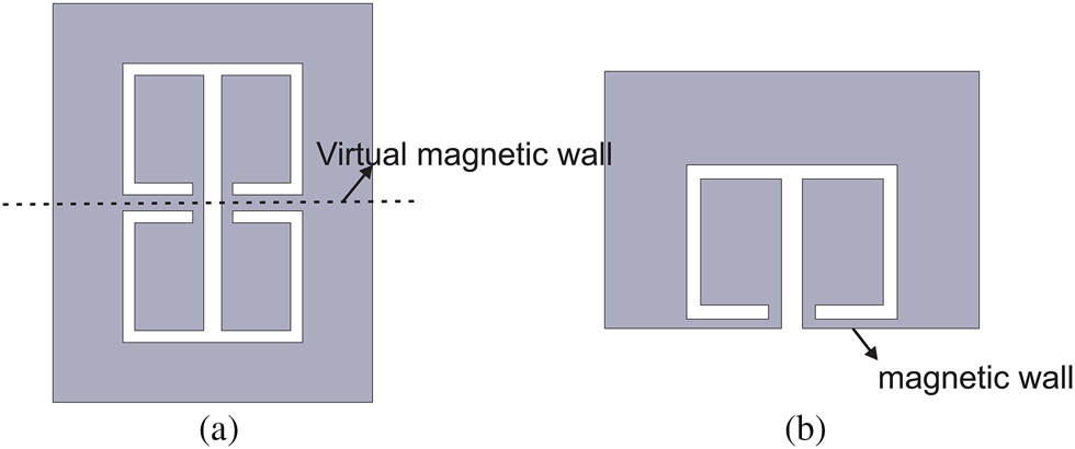
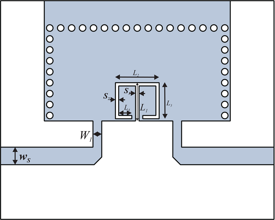
HMSIW cavity is loaded with the half-mode DGS unit-cell to generate a passband at low frequency. The half-mode DGS is extracted by cutting back-to-back connected E-shaped DGS along the magnetic wall, as shown in Fig. 2. The proposed novel half-mode DGS size is half, and its resonant characteristics are almost similar to the original back-to-back connected E-shaped DGS [Reference Cai, Qian, Cao, Zhang and Yang26]. From Figs 1(a) and 2(b), both the HMSIW cavity and half-mode DGS are sharing the magnetic wall. Therefore, the half-mode DGS unit-cell is loaded into the HMSIW cavity, as shown in Fig. 3. This structure is simulated with the HFSS EM-simulator.
(a) Back-to-back connected E-shaped DGS unit-cell. (b) Half-mode DGS unit-cell.

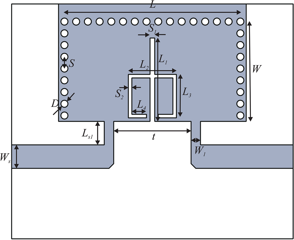
HMSIW cavity with half-mode DGS unit-cell (W = 8.5 mm, L = 15 mm, S = 1.0 mm, D = 0.6 mm, W s = 2.0 mm, W 1 = 0.8 mm, L 11 = 4.0 mm, L 2 = 4.1 mm, L 3 = 3.7 mm, L 4 = 1.35 mm, S 1 = 0.4 mm, t = 6 mm, and S 2 = 0.3 mm).

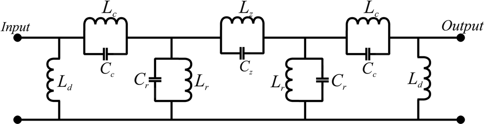
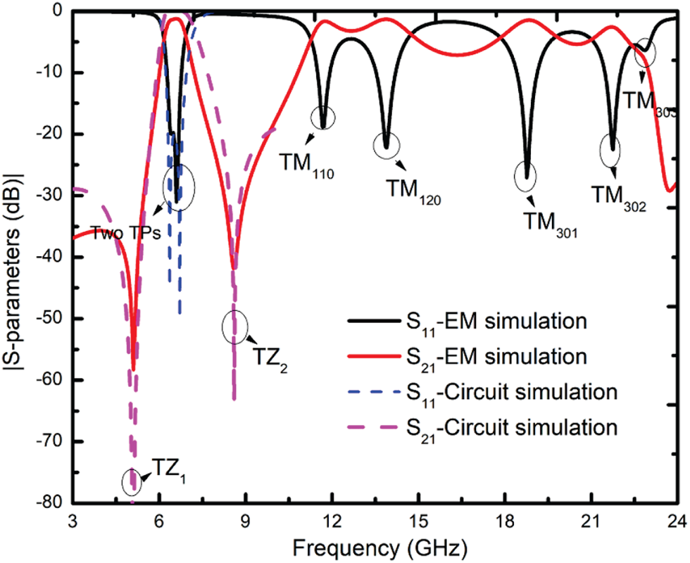
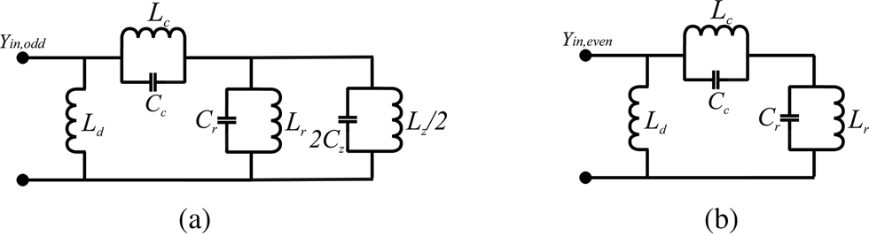
The equivalent circuit of HMSIW cavity with half-mode DGS is shown in Fig. 4. The HMSIW cavity is like an ordinary two-wire transmission line loaded with via-walls which provide a shunt inductor (L d). Half-mode DGS is constituted as the shunt connected resonant tanks (L r and C r). The shunt connection of L z and C z models the mixed-coupling between DGS resonators. L c and C c indicate magnetic and electric coupling, respectively at feedlines. It is noted that this circuit model is a simplified version, and it is simulated by using an advanced design system circuit simulator. In Fig. 5, the electromagnetic (EM) and circuit simulations of fig. 3 and fig. 4, respectively, are compared. Therefore, this circuit is correct and fully capable of explaining the transmission characteristics. The even- and odd-mode analysis method has been used to find the resonant frequencies (f odd and f even) and two TZs f zp1 and f zp1 [Reference Xu, Ma, Meng and Yeo4]. The even and odd mode circuits are shown in Fig. 6. The even and odd mode frequencies are obtained by finding the input admittance and solving the equation of Im(Y in)=0 using respective equivalent circuits:

Equivalent circuit of the half-mode DGS unit-cell. (The element values are: Lc = 1.26 nH, Cc = 0.77 pF, Ld = 3.1 nH, Lz = 1.04 nH, Cz = 0.33 pF, Lr = 0.58 nH, and Cr = 0.87 pF.)


Equivalent circuits of Fig. 4: (a) odd mode and (b) even mode.

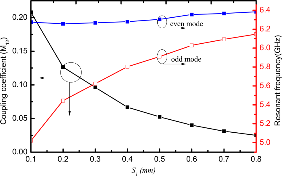
The coupling coefficient (M12) varied with S 1.

On the other hand, Y in,even = Y in,odd condition gives the TZs:

As is well known, the coupling coefficient (K) between two resonators and external quality factor (Q ext) can be evaluated by [Reference Hong and Lancaster27]


where f 0 is the center frequency (CF) and $f_{3\hbox {-dB}}$ is 3-dB bandwidth. Here, the DGS length should be set to a quarter wavelength at the CF of passband. Then, the design parameters could be calculated using Q ext and M ij from prescribed specifications of the passband using the synthesis procedure described in [Reference Hong and Lancaster27].
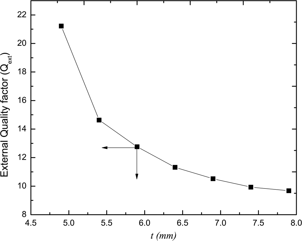
The coupling coefficient (M 12) = 0.0802 and external quality factor (Q ext) = 13.76 are calculated using lowpass prototype element values [Reference Hong and Lancaster27] for 20 dB return loss bandwidth 4.83% and CF 6.2 GHz. Figures 7 and 8 show the extraction of coupling coefficient with respect to S 1 using equation (5) and the extraction of an external quality factor with respect to t using equation (6), respectively. The parameters S 1 and t are chosen based on M 12 and Q ext values. As shown in Fig. 5, the odd and even mode frequencies of the proposed DGS are 6.1 and 6.3 GHz, respectively. The TZs are at 4 and 8 GHz, which increase roll-off characteristics of the first passband.
The variation of external quality factor (Qext) with t.

HMSIW cavity with slot perturbation
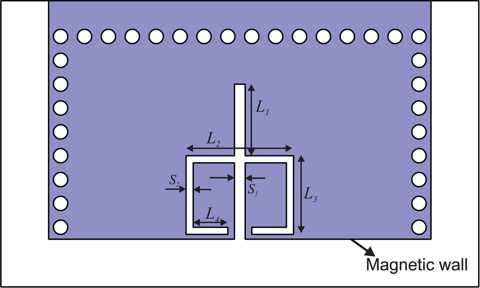
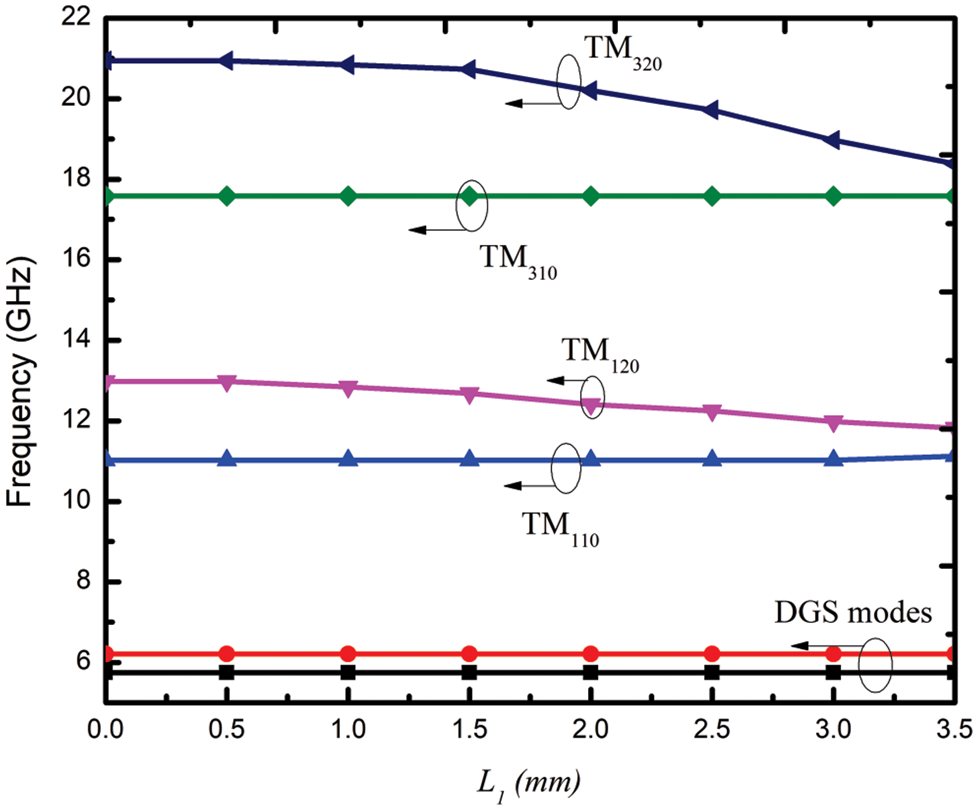
HMSIW cavity's first four mode frequencies are pushed up to 11, 13, 17.5, and 21 GHz, due to restricts of the fields to a smaller region and change of current distribution by DGS unit-cell. Moreover, TM 130 mode current distribution is not supported by DGS unit-cell. In order to make a dual passband using a mode shift technique, a slot line is etched along with half-mode DGS on the top layer of HMSIW cavity, as shown in Fig. 9. Fig. 10 shows the impact of slot line on resonant modes of the cavity. The slot line shifts TM 120 and TM 320 modes resonant frequency effectively, while the resonant frequencies of TM 110 and TM 310 modes are almost unchanged. The reason is, the etched slot does not affect the current distribution of TM 110 and TM 310 modes, whereas the etched slot perturbs the current distribution of TM 120 and TM 320 modes. Therefore, the slot line length (L 1) and the feed position (t) are fixed to prescribed fractional bandwidths with return loss better than 20 dB. However, the DGS modes are constant for slot length. Therefore, the DGS modes give passband at low-frequency, TM 110 and TM 120 make second passband and TM 310 and TM 320 generate third transmission band.
HMSIW cavity with slot perturbation (W = 8.5 mm, L = 15 mm, S = 1.0 mm, D=0.6 mm, L 1 = 3.1 mm, L 2 = 4.1 mm, L 3 = 3.7 mm, L 4 = 1.35 mm, S 1 = 0.4 mm, and S 2 = 0.3 mm).

The variation of frequencies of the first four resonant modes versus L 1.

Triple-band filter
The proposed triple-band filter configuration is shown in Fig. 11. It consists of half-mode DGS unit-cell and HMSIW cavity with slot perturbation. The DGS modes give the first band, and the HMSIW cavity with slot line generates the second and third transmission bands. The proposed HMSIW cavity with DGS unit-cell is excited with step impedance I/O feedlines.
Layout of the proposed triple-band structure.

Design procedure
The design procedure of triple-band BPF based on the proposed multi-mode HMSIW cavity can be epitomized as follows:
(1) Determine the initial dimensions of the HMSIW cavity, as discussed in section “HMSIW cavity” according to the CFs of the second and third passbands.
(2) Determine the DGS length (L 11 + L 2/2 + L 3 + L 4), which is nearly a quarter-wavelength at first passband CF.
(3) Determine the design parameters consisting of Q ext and M ij from prescribed specifications, including the CF and the bandwidth of the first passband using the synthesis procedure described in [Reference Hong and Lancaster27].
(4) Extract the curves of the external quality factor Q ext and the coupling coefficients M ij in the first passband versus the positions of the feeding ports t and the coupling slot S 1, respectively. The parameters S 1 and t selection depends on M 12 and Q ext values.
(5) Adjust the length of the etched slot (L 1) and the feed position (t) to achieve prescribed fractional bandwidths of second and third passbands with return loss better than 20 dB.
(6) Tune filter parameters to optimize the performance.
As an example, a tri-band filter is designed with the targeted specifications as follows:
(1) passband 1: 6.2 GHz (FBW: 0.09);
(2) passband 2: 12.5 GHz (FBW: 0.062);
(3) passband 3: 18.5 GHz (FBW: 0.05);
(4) in-band return loss: 20.0 dB.
First, the initial dimensions of the HMSIW cavity are determined according to TM 110 and TM 310 modes resonant frequencies at 8.6 and 18.3 GHz, respectively, using equation (2). The parameters are (in mm): diameter of vias D = 0.6, pitch S =1.0, L = 15, and W = 8.5. Second, the initial length of half-DGS is calculated at the first CF which is nearly a quarter-wavelength. The calculated DGS length is L 11+L 2/2+L 3+L 4 = 36 mm. Then, the coupling coefficient (M 12)=0.0802 and external quality factor (Q ext)=13.76 are calculated using lowpass prototype element values [Reference Hong and Lancaster27] of 20 dB return loss bandwidth 4.83% and CF 6.2 GHz. The parameters S 1 and t are chosen to be 0.3 and 6 mm, respectively based on M 12 and Q ext values from Figs 7 and 8. Next, the etched slot length (L 1) and the feed position (t) are chosen as 6.8 and 7 mm, respectively based on fractional bandwidths of second and third passbands with return loss better than 20 dB.
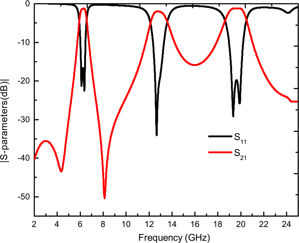
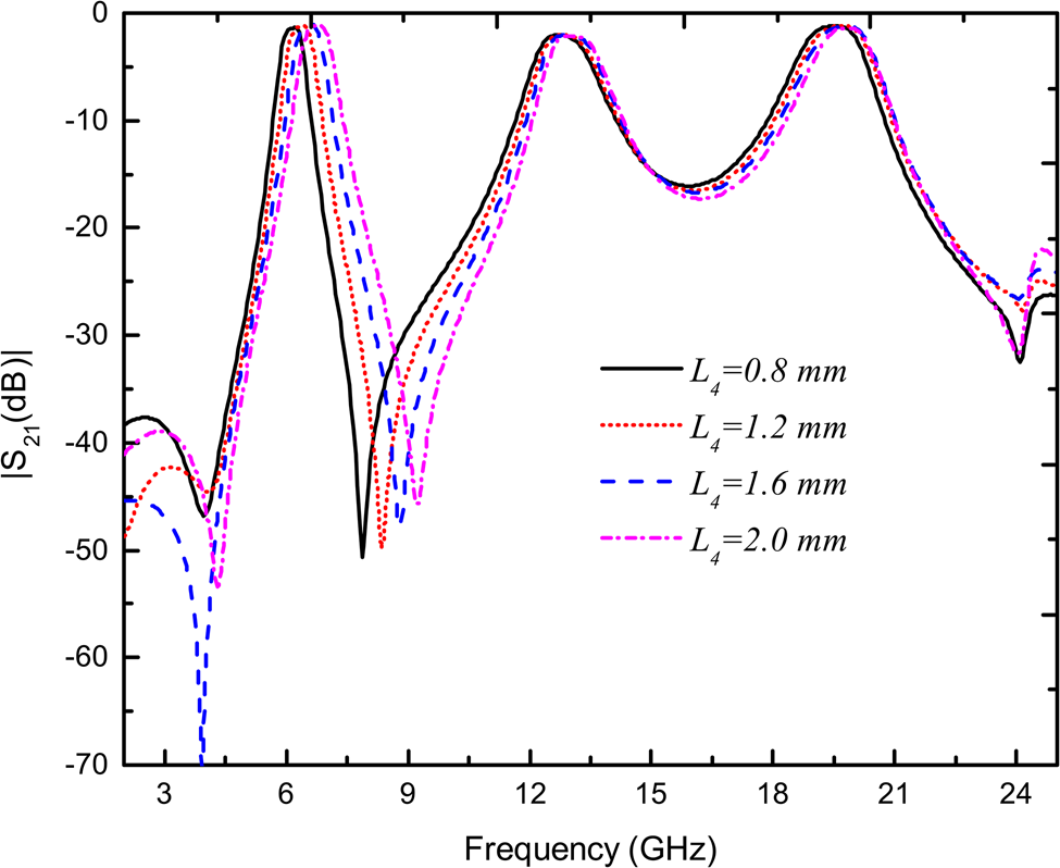
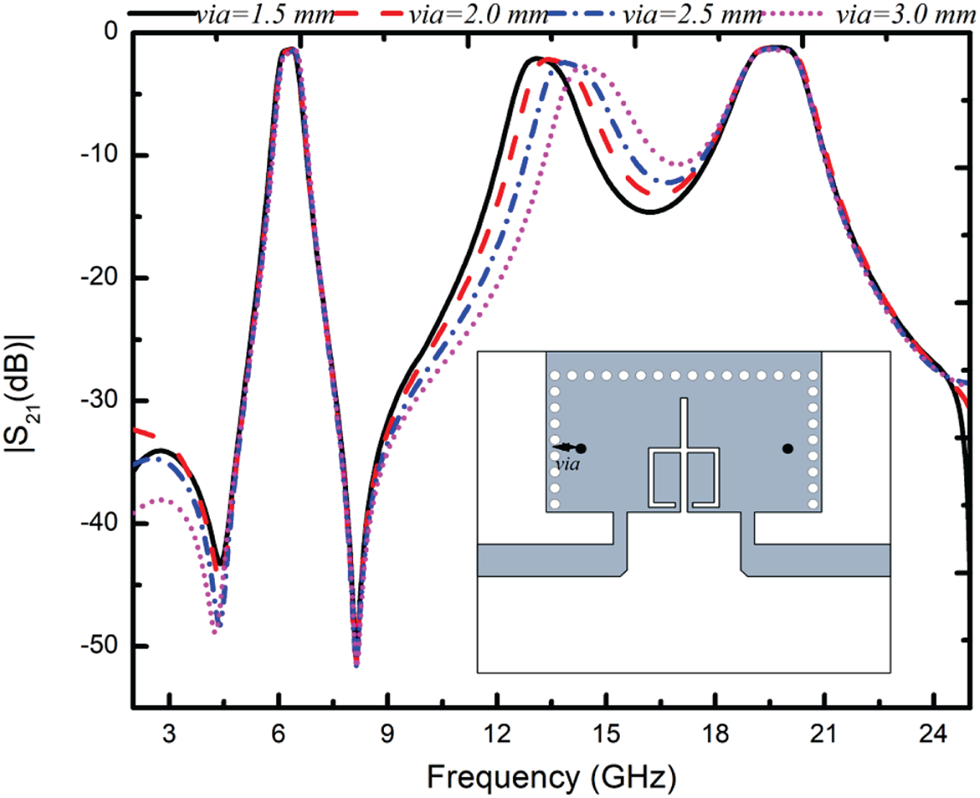
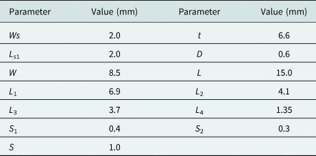
All dimensions are optimized to obtain better characteristics in three bands using the HFSS electromagnetic (EM) simulator. The dimensions are given in Table 1. The EM-simulated S-parameters of Fig. 11 are shown in Fig. 12. The first, second, and third passband CFs are 6.2, 13.0, and 19.1 GHz, respectively. There are two TZs at 4 and 8 GHz due to half-mode DGS, which provide attenuation of 30 dB from DC to 5 GHz and 20 dB from 7 to 10.4 GHz, respectively. The HMSIW cavity does not support the modes which do not satisfy magnetic wall conditions. Therefore, the significant separation is obtained between the second and third passbands. The first passband can be tuned by changing L 4, while the second and third passbands are almost constant, as shown in Fig. 13. In Fig. 14, the vias are placed where they show the effect on second passband modes and do not affect third passband modes. By changing the position of vias (via), the second passband is tuned, and the first and third passbands are almost constant. Therefore, the bands can be tuned independently.
EM-simulated S-parameters of Fig. 11.

Frequency response of the BPF with varied L 4.

Frequency response of the BPF with varied via.

Dimensions of the proposed structure

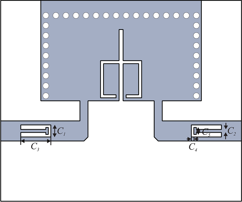
As shown in Fig. 12, the attenuation between the second and third passbands is around 15 dB. To improve this attenuation, a notch band is needed between the second and third passbands. The well-known techniques are conventional open-circuit stub, spur line, and embedded open-circuited stub [Reference Hong and Lancaster27]. The embedded open-circuited stub shows good performance and does not affect the main transmission line characteristics because the majority of the current flows around the edges of the microstrip line. In Fig. 15, T-shaped embedded open-circuited stubs are loaded in input/output (I/O) feedlines to get wideband notch characteristics. Here, the stub line width should be small to get high characteristic impedance, and the length of the stub line depends on the notch band CF. The simulated S-parameters are shown in Fig. 16, which shows that the embedded T-shaped open-circuited stub provided 45 dB attenuation between the second and third passbands.
Embedded T-shaped open-circuited stub in feedlines (C 1 = 1.2 mm, C 2 = 0.3 mm, C 3 = 3.0 mm, C 4 = 0.25 mm, and C 5 = 0.7 mm).

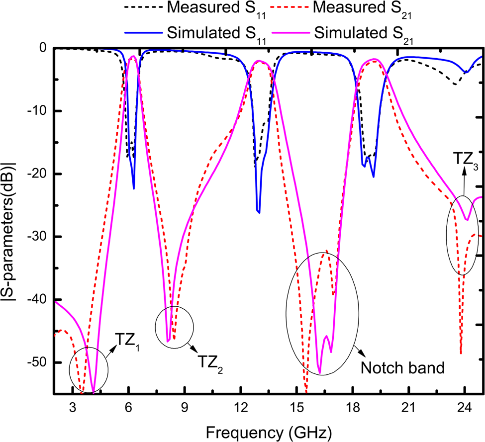
Measured and simulated S-parameters.

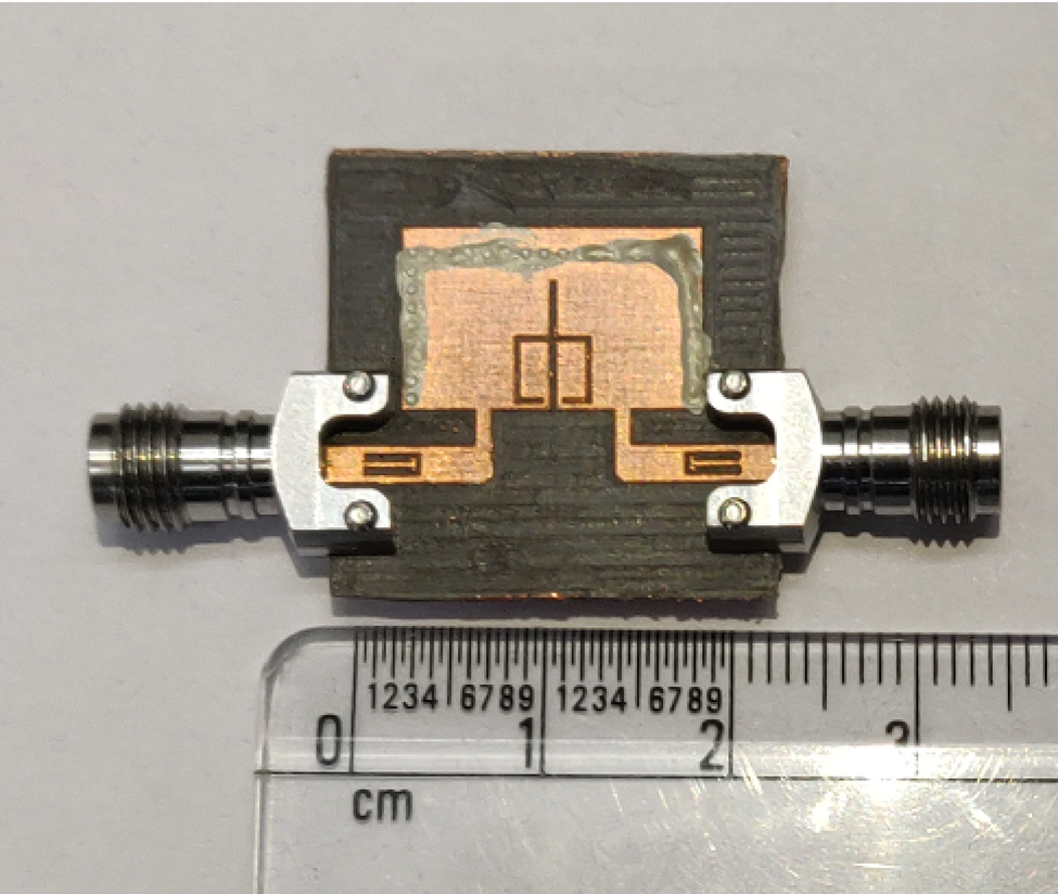
Photo of fabricated triple-band BPF.

Fabrication and measurement
The proposed final structure of the triple-band HMSIW is shown in Fig. 15, which is fabricated on the RT/duroid 5880 substrate with a thickness of 0.508 mm using low-cost single-layer PCB technology. The proposed filter is fabricated using the LPKF milling machine, and the discrete vias of the HMSIW cavity are metalized with silver paste, as shown in Fig. 17. The area of the filter without feedlines is 8.5 × 15 mm2(0.12$\lambda _{g}^{2}$ ), where λg is guided wavelength at first passband CF 6.25 GHz. The S-parameters are measured using 1.85 mm end-launch connectors and vector network analyzer (Agilent N5247A). As shown in Fig. 16, the measured results are comparable to the simulation results and describe the triple-band characteristics.
The CFs of the passbands are 6.28, 13, and 19.12 GHz. The simulated insertion losses are 1.3, 1.9, and 1.75 dB, while the measured insertion losses, including end-launch connector loss, are 1.6, 2.5, and 2.2 dB. The measured results show more than 13 dB return loss in the three passbands. The measured 3-dB fractional bandwidth of passbands are 9.5, 6.2, and 4.5%, while the simulated 3-dB fractional bandwidth of passbands are 8.5, 7.2, and 6.1%. The TZs TZ 1 and TZ 2 at 3.52 and 8.44 GHz help to get better roll-off characteristics of the first passband. The fabrication error in DGS unit-cell created a little shift in the position of TZs. Moreover, the embedded T-shaped stub in feedlines provided the rejection of 54.8 and 39.3 dB between the second and third passbands due to notch bands at 15.52 and 16.96 GHz, respectively. The notch band frequencies have slightly deviated from simulation results caused by fabrication tolerance. The transmission zero TZ 3 be found at 24.16 GHz due to higher-order modes and improved stopband performance of the third passband with an attenuation of 27.34 dB. Therefore, the measured results recommend that the proposed filter has a triple-band response with better stopband performance.
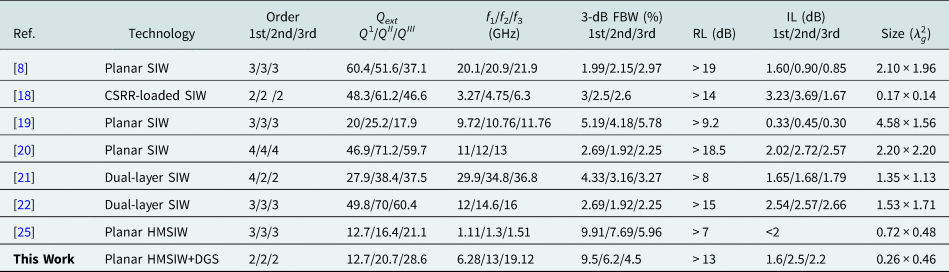
The proposed filter is compared with the state-of-art designs of SIW triple-band filters in Table 2. The authors of [Reference Chen, Wu and Li8, Reference Esmaeili and Bornemann19, Reference Tsai, Shen, Chen, Huang and Wu21, Reference Shakib, Sekar and Entesari25] discussed triple-band design by introducing finite transmission zero into a single passband. This technique is not applicable in the case of wide-spaced passbands, and circuit size is also significant. Different types of complementary split ring resonators (CSRRs) loaded into SIW to generate multiple passbands below the cutoff frequency [Reference Dong, Wu and Itoh18]. This method is not preferable at high frequencies. In [Reference Xie, Zhou, Zhou and Wu20], triple-mode cavities have been used to make triple-band BPFs. However, the passbands are very close. Guo et al. [Reference Guo, Zhu and Wu22] discussed triple passband design using dual-layer SIW technology. For the first time, a triple-band filter is designed with HMSIW cavity and DGS. The advantages are widely separated bands, acceptable insertion loss, and compact size.
Comparison with state-of-art designs

λg is the guided wavelength at first passband CF.
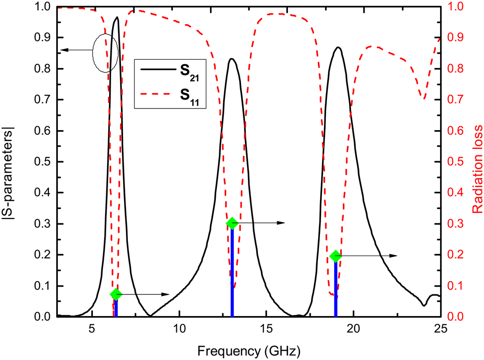
On the other hand, the half-mode DGS slot is loaded on the upper layer of the HMSIW structure. This DGS slot is the source of radiation in the upper half-space. Therefore, the radiation loss could be calculated as follows:

The simulated radiation loss is shown in Fig. 18, which is under the conditions of a lossless substrate (tanδ = 0) and metal. The radiation losses in three bands are 0.072, 0.28, and 0.18 and the insertion losses are approximately 0.3, 1.37, and 1.0 dB due to only radiation. Therefore, the radiation loss effect is more at higher frequency bands because of the perturbation of current distribution by DGS and open-end of HMSIW cavity.
Radiation loss.

The noticed limitations of our proposed triple-band filter are individual bandwidth control of second and third passbands and the radiation loss. Nevertheless, the structure is simple and compact.
Conclusion
A compact triple-band passband filter is discussed. The first passband is given at 6.28 GHz by half-mode DGS which is etched on the top layer of the cavity and does not occupy extra space. Therefore, the proposed design is compact. The second and third passbands are due to the first four modes of HMSIW cavity with slot perturbation. The passbands are widely separated because the HMSIW cavity does not support all the modes of SIW. Therefore, the proposed structure gives three widely separated passbands with small size and less cost.
 Sambaiah Pelluri received his B.tech. in electronics and communication engineering from Vignan's Engineering College, Guntur, India, in 2008, and his M.tech. in Electronic Design and Technology from the National Institute of Technology, Calicut, India, in 2010. He has been an assistant professor with the Department of Electronics and Communication Engineering, Vignan's Foundation for Science, Technology and Research, Vadlamudi, India, since 2010. He is currently pursuing his Ph.D. with IIT Roorkee under QIP scheme, Roorkee, India. His current research interests include developing novel passive components and active devices for microwave and millimeter-wave integrated circuits.
 M.V. Kartikeyan has received his M.Sc. in physics, and Ph.D. in electronics engineering from IIT (BHU) Varanasi, Varanasi, India, in 1985 and 1992, respectively. He has been a Full Professor with the Department of Electronics and Communication Engineering, IIT Roorkee, Roorkee, India, since 2009. His current research interests include millimeter/THz wave engineering (electron cyclotron masers, high power devices, and components), metamaterials and fractals, planar microstrip antennas and filters, MICs, and RF and microwave design with soft computing techniques. Prof. Kartikeyan is a Fellow of IEEE, Fellow of the IET (UK), Institution of Electronics and Telecommunications Engineers (India), Institution of Engineers (India), and Vacuum Electronic Devices and Applications Society (India).