I. INTRODUCTION
Due to rapid development in the field of wireless application, the multifunctionality is a necessity for the system. There are numerous wireless communication systems in our daily lives such as HDTV broadcast, online game, real time video streaming, cellular radio systems, mobile, satellite systems, wireless local area networks, etc. All these systems are still undergoing a great progress, with constantly promising novel solutions. The multiple-input–multiple-output (MIMO) systems offer a substantial increase in channel capacity without the need for additional bandwidth or transmit power. By deploying several antennae for transmission to achieve an array gain and diversity gain, spectral efficiency can be improved. Various MIMO wireless systems have demonstrated till date. A coplanar multiband MIMO operating at GSM to LTE-D band consists of folded monopole and beveled rectangular patch. It has good performance inlet reference signal receiving power (RSRP) and download speed and upload speed [Reference Yang, Chu and Mao1]. An antenna consisting of an array of two printed dipoles is reconfigured using PIN diode to improve link capacity. It has an average improvement of 10 and 8% in link capacity and signal-to-noise ratio, respectively [Reference Piazza and Kirsch2]. The antenna can be designed using conical two-port antenna that can be replicated and concatenated together to form MIMO with antenna densities of up to 22 antennae per square wavelength [Reference Soltani and Murch3]. An antenna system consisting of PIN diode operating on 2.3 and 3.5 GHz and IWO (invasive weed optimization) is used for two-channel MIMO antenna array [Reference Ghasemi and Ghahvehchain4]. A frequency reconfigurable MIMO antenna is designed to minimize antenna volume and to compensate for user-oriented impedance detuning losses [Reference Rasilainen and Lehtovuri5]. A frequency reconfigurable slot antenna achieves pattern diversity and improves performance by placing two identical slot antennas separated by quarter wavelength suitable for frequency 5.2 GHz [Reference Mubasher and Wang6]. A reconfigurable wheel antenna array that operates in S – band, and X – the band has multiple resonating frequencies using patch antenna with PIN diode [Reference Ramakrishna and Pandhripande7]. In general, sharing of common ground and near-field coupling causes mutual coupling between closely placed antennae [Reference Pozar8]. This can degrade the performance of antennas. Significant research had been done to reduce mutual coupling that is to increasing isolation [Reference Lim and Jin9]. There are various ways of reducing mutual coupling. By having band-notched quarter wave slot line on the ground plane and locating PIN diode, isolation can be increased. The geometry of defected ground plane can be modified [Reference Zhang, Ying, Xiong and He10, Reference Zhang, Khan and He11]. Again, by adding electromagnetic band-gap structure (EBG), unwanted propagation at the surface can be reduced thus minimizing mutual coupling [Reference Yang and Rahmat-Samii12, Reference Dadashzadeh, Dadgarpour, Jolani and Virdee13]. The slot cutting on resonating antenna element is proposed in [Reference Ayatollahi, Rao and Wang14]. In [Reference Mak, Rowell and Murch15], ground branch technique for dual element Inverted F Antenna is discussed.
One of the challenges of the multiple application systems is the design of the multiband antenna. Multiband antennae are considered to be a good solution for supporting many different applications with a good performance at all frequency bands. Bluetooth and WLAN operate in 2.4 GHz industrial, scientific and medical (ISM) band (frequency range 2.4–2.5 GHz). Mobile WiMAX operating bands are 2.3 GHz (frequency range 2.3–2.4 GHz) and 3.5 GHz (frequency range 3.4–3.6 GHz) [Reference Haraz and Sebak16]. Methods for increasing capacity even further are still required however and this includes increasing the current number of antennas at the mobile device from 2 to 4 as in 802.11ac and LTE [Reference Werner, Furuskog, Riback and Hagerman17, Reference Furuskog, Werner, Riback and Hagerman18].
One common use of antenna is in vehicular communication like trains GPS system on elevated railways. The precise vehicular antenna should be selected to cover all frequencies providing wireless services, including GPS and Wi-Fi. This paper introduces frequency reconfigurable MIMO antenna with pentagon slot as radiating element along with monopole. The proposed antenna is capable of achieving good isolation of |S 21|<−30 dB for all operating frequencies. It has more bandwidth which is required to provide seamless internet access for the mobile devices, a multiband antenna for GPS, Wi-Fi, and mobile operation. This antenna can be ideal for fleet management systems, Wi-Fi routers, outdoor applications etc. The details and experimental results for the proposed MIMO antenna are presented and analyzed in this paper. The novelty of this work is there is an enhancement of bandwidth according to the need of application with the use of PIN diodes. This paper is organized as follows. In Section II, the antenna design of pentagon slot resonator antenna for MIMO is described. In Section III, simulation results of pentagon slot resonator antenna for MIMO are presented. In Section VI, result and discussion of pentagon slot resonator antenna for MIMO are described. Finally, conclusions are drawn in Section V.
II. ANTENNA DESIGN
A pentagon slot resonator with the shape and dimensions similar to that in [Reference Sung19] is adopted. The antenna is designed on (L × W × h) 60 × 120 × 1.6 mm3 on the substrate FR4 with permittivity of 4.4. These dimensions of the antenna are calculated using basic formulas, which are mentions in books of Constantine A. Balanis and J.D. Kraus by considering minimum and maximum operating frequency (1.5 and 2.4 GHZ) within the range of 1–3 GHz as in equation (1). For an effective resonator, a width and length which lead to good radiation efficiency is calculated by
 $$\eqalign{& L_{eff} = \displaystyle{c \over {2f_r\sqrt {\varepsilon _{reff}}}}, \quad \varepsilon _{eff} = \displaystyle{{\varepsilon _r + 1} \over 2} + \displaystyle{{\varepsilon _r - 1} \over 2}\left[ {1 + 12\left( {\displaystyle{h \over w}} \right)} \right]^{ - 1/2}, \cr & \Delta L = 0.421h\left[ {\displaystyle{{(\varepsilon _{eff} + 3)\left( {(w/h) + 0.264} \right)} \over {(\varepsilon _{eff} - 0.258)\left( {(w/h) + 0.8} \right)}}} \right], \cr & W = \displaystyle{{\; C} \over {2f_r}}\sqrt {\displaystyle{2 \over {\varepsilon _r + 1}}}, z = \displaystyle{{377} \over {\sqrt {\varepsilon _r((w/t) + 2)}}}} $$
where L-length of the patch antenna, W is the width, H the height, εr the dielectric constant of the substrate, f r the resonating frequency, εeff the effective dielectric constant, t the thickness of the substrate, Z the characteristics impedance, and w the width of the feedline.
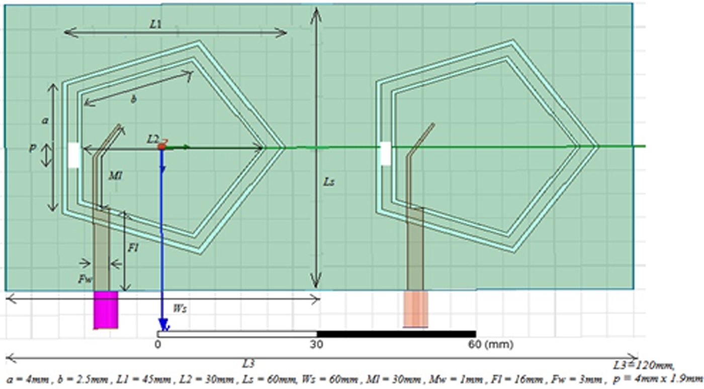
The proposed frequency reconfigurable MIMO antenna geometry is as shown in Fig. 1. The inner pentagon slot resonator, which resonates at 2.4 GHz frequency has length b of 2.5 mm and that of outer pentagon slot resonator a has 4 mm to resonate at the 1.5 GHz frequency. The width of each resonating slot is 1 mm. The pentagonal radiator is fed by (F l × F w) 16 mm×3 mm microstrip feed line of 50 Ω on opposite side of the substrate. The length and width of the monopole are (M l × M w) 30 and 1 mm, respectively, to have omni-directional radiation. The dual-band reconfigurable antennas have attracted attention because it can be used for different applications at different times and therefore are likely to be compact. This geometry gives dual-band operation [Reference Borakhade and Pokle20]. To implement reconfigurability, the ideal short may be replaced by PIN diode. The high switching speed, very small resistance and capacitance in ON and OFF states, reliability, compactness make it appropriate for RF switching applications. In order to decide the best possible positions of the PIN diodes, the current distribution of antenna is taken into account. The current distribution of proposed antenna is along the edges of pentagon resonator slot. So by removing some portion of metallization where the current density is low, we can increase the effective path of surface current. Hence, the effective length of current distribution path is increased by inscribing PIN diode at patch pentagon slot in a ground plane where the current density is low. Thus, more energy is transmitted due to the closed path provided by the diode. This current path contributes to enhancing bandwidth at the highest edge of the frequency band. This is done by using SMP 1320 series SC – 79 of plastic packed, surface mount PIN diode is used from Skyworks Technologies. In forward bias, the diode has a forward resistance of 0.9 Ω and inductance of 0.6 µH. The PIN diodes are placed on a patch of dimension 4 mm×1.9 mm between the pentagon slot resonators. For MIMO application, to optimize the isolation characteristics for multiple frequencies and to enhance the gain, the two-reconfigurable pentagon slot resonator is placed symmetrically separated by distance λ/2 from each other which is 60 mm. The operating frequency of the antenna is 1.0–3.2 GHz taking into deliberation of Bluetooth, Wi-Fi and GPS, and PCMCIA card applications and also WLAN. The proposed frequency reconfigurable MIMO antenna geometry is as shown in Fig. 1.
Proposed antenna dimensions of pentagon slot resonator MIMO antenna.

III. SIMULATION RESULT
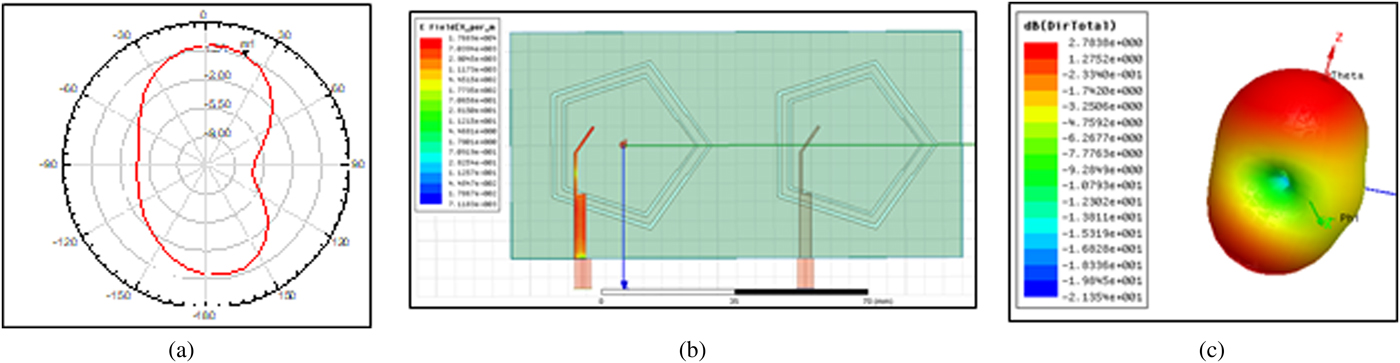
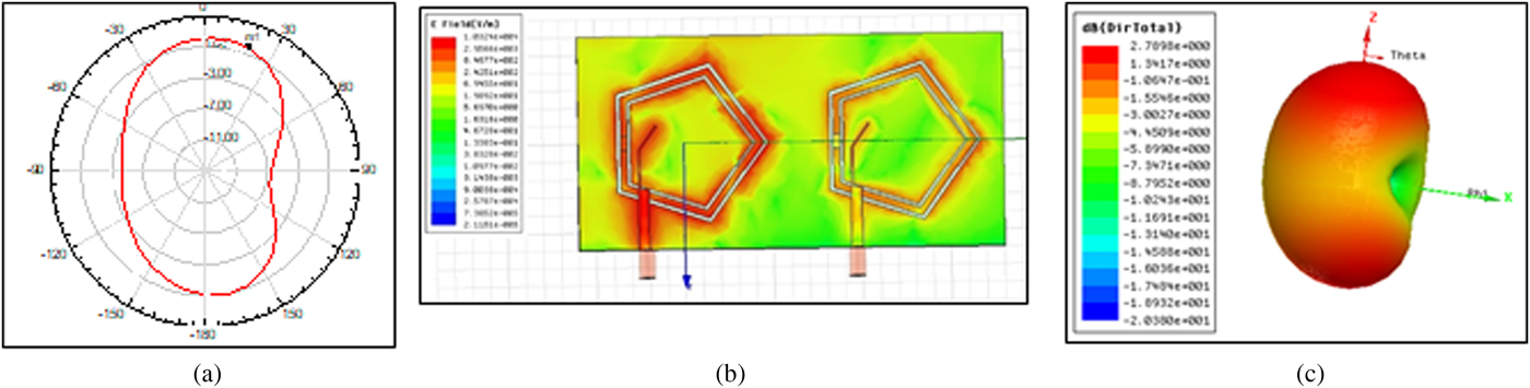
The simulation results are obtained using Ansoft HFSS, which is based on the finite-element method (FEM). To switch between different frequencies bands, PIN diodes are inserted between the radiating slots. To simplify the design and discussion, the width of the feed line is chosen to be 3 mm, which corresponds to the characteristic impedance of 50. The radiation pattern current distribution and three-dimensional (3D) polar plot for MIMO with PIN diode are shown in Figs 2(a), 2(b) and 2(c). The radiation pattern current distribution and 3D polar plot for MIMO without PIN diode are as shown in Figs 3(a), 3(b), and 3(c), respectively. The proposed antenna in this paper achieves reconfigurability to attain high bandwidth. After inserting PIN diodes bandwidth is 207 and 253 MHz at 1.53 and 2.59 GHz, respectively.
3D Polar plot and radiation pattern and current distribution of MlMO antenna without switch
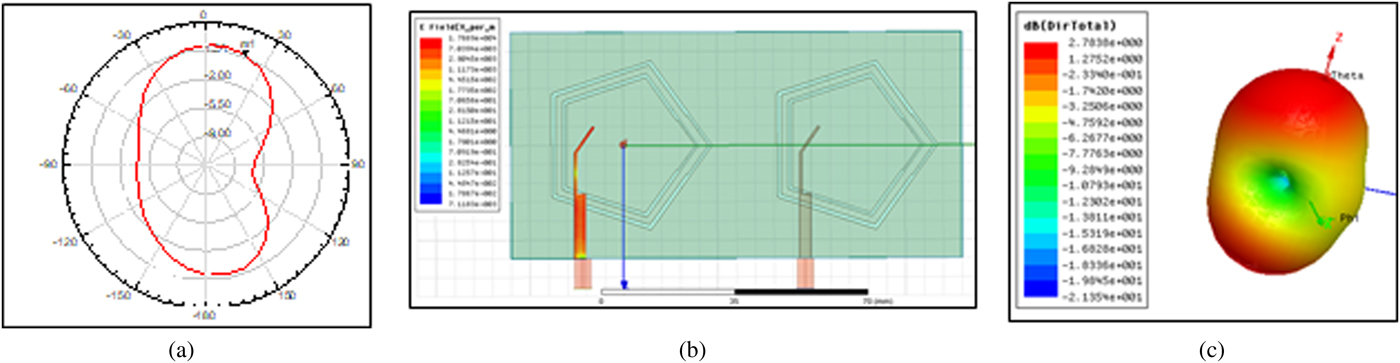
Radiation pattern and current distribution and 3D Polar plot of MIMO antenna with switch

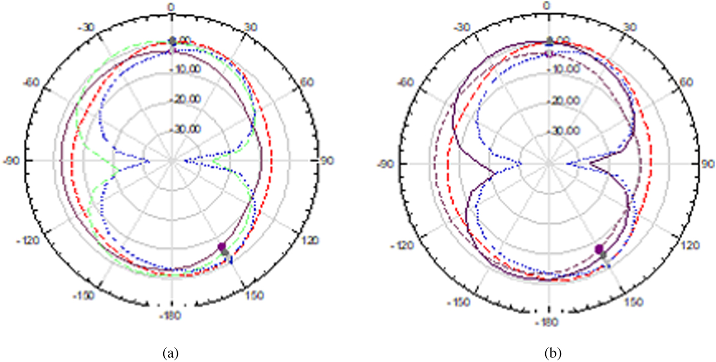
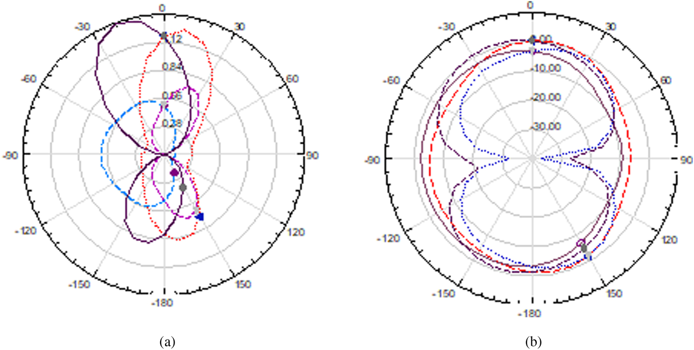
The effect of PIN diode on different parameters of antenna like S-parameter, VSWR, bandwidth, etc. are analyzed by comparing MIMO without switch and MIMO with a switch are listed in Table 1. The value of VSWR is found to be 1.3 and 1.41 at frequencies 1.48 and 2.58 GHz respectively when no diodes are inserted and are 1.28 and 1.44 at 1.53 and 2.58 GHz respectively when both diodes are ON. The red and yellow regions in current distribution plot signify the strongest E-field while the blue or green regions signify the weakest field. It shows that when both the diodes are OFF the E-field on the antenna is low whereas when both are ON it is highest. All the plots are normalized to the same field strength. For different biasing conditions of PIN diode, the radiation pattern for phi at 0° and 90° which gives co-polarization and theta at 0° and 90° showing cross-polarization when both diodes are in ON state are shown in Figs 4(a) and 4(b) and that for when PIN diode 1 is OFF and other is ON when both PIN diodes are OFF are shown in Figs 5(a) and 5(b), respectively.
MIMO antenna radiation pattern for co-polarization when both PIN diodes are ON and when PIN diode 1 is ON and other is OFF

MIMO antenna radiation pattern for co-polarization when PIN diode 1 is OFF and other is ON when both PIN diodes are OFF

Different parameters of MIMO antenna with and without PIN diode acting as a switch.

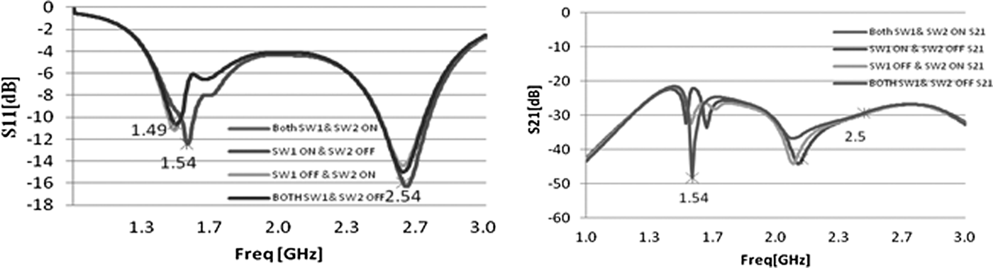
The antenna also has monopole which gives omni-directional characteristics. When both PIN didoes are in ON bandwidth obtained 207 and 252 MHz at 1.5 and 2.5 GHz frequencies respectively which are shown in Fig. 6(a) by simulated S-parameters S 11 for different operating conditions of PIN diodes of pentagon slot resonator MIMO antenna and that of isolation is shown in Fig. 6(b). With both diodes in OFF state bandwidth obtained are 67 and 207 MHz for the same set of frequencies. The frequency will be more dominating with the different biasing arrangement of PIN diode. The diode makes the antenna reconfigurable and turns ON and OFF resonating frequencies with enhanced bandwidth.
Simulated S11 (a) and S21(b) results of the Frequency Reconfigurable MIMO antenna with different switch combinations.

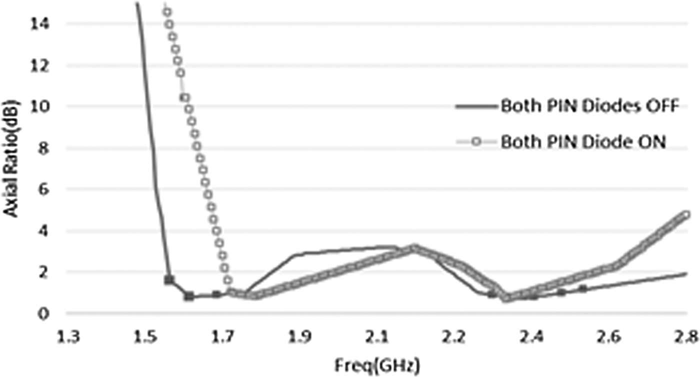
In this paper, the circularly polarized reconfigurable antenna as in [Reference Sung19] is proposed. The circular polarization (CP) is obtained by introducing proper asymmetry to the proposed slot antenna, and the symmetry of the structure can be perturbed. Figure 7 shows the axial ratio of the proposed antenna from frequency 1–3 GHz. Due to the structure proportion, the S 11 and the axial ratio are maintained during switching between the different biasing states of PIN diode, which has been the advantage of this design.
Simulated axial ratio of the proposed antenna when both PIN didoes are OFF and when bo1h PIN diodes are ON

Another important parameter for designing MIMO is envelope correlation coefficient (ECC), which is a measure of how radiation patterns of antennas are independent of each other. For diversity and MIMO application, the correlation coefficient between the two antennas is another vital factor in the usefulness of antenna. It can be computed from S-parameters. For two antennas, it is calculated using the formula in equation (2). This equation provides adequately precise results in many enclosed environments with rich multipath propagation [Reference Votis and Tatis21]. It is calculated and found to be in the range of 0.001–0.004 which means radiation pattern of two antennas are independent of each other and do not interfere.
 $$\rho _e = \displaystyle{{ \vert S_{11}^* S_{12} + S_{21}^* S_{22} \vert ^2} \over {(1 - \vert S_{11} \vert ^2 - \vert S_{21} \vert ^2)(1 - \vert S_{22} \vert ^2 - \vert S_{12} \vert ^2)}}.$$
IV. RESULTS AND DISCUSSION
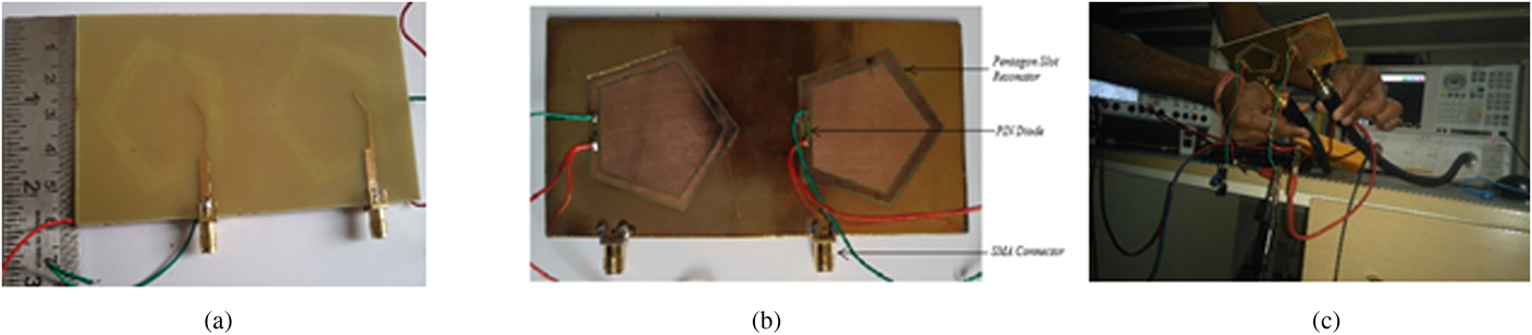
To certify the simulated results, a prototype of the proposed antenna was fabricated. The top view as in Fig. 8(a) and the bottom view in Fig. 8(b) along with the testing setup of the prototype as in Fig. 8(c) are shown. The antenna is tested on vector network analyzer (VNA Agilent N9923A). Also, to minimize simulation time, there are neither DC lines nor DC coupling component included during simulation.
Practical prototype of Proposed Frequency Reconfigurable MIMO antenna (a) Top view (b) Bottom View and (c) Testing Setup for antenna

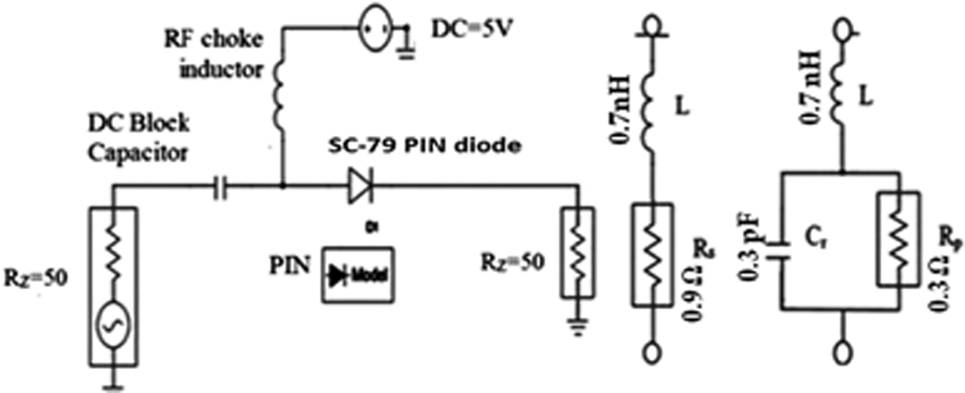
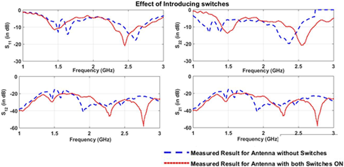
In Ansoft HFSS, PIN diodes are modeled using lumped RLC boundary conditions so as to simulate and analyze the effect of actual PIN diode. Here SMP 1320 series SC–79 PIN diode are used. In forward bias condition, the diode is modeled with the forward resistance of 0.9 Ω and inductance of 0.7 nH as shown in Fig. 9. In reverse bias condition, the PIN diode has a reverse parallel resistance of 0.3 Ω, the capacitance of 0.3 pF and inductance of 0.7 nH. When PIN diodes are in OFF state, the insertion loss is below −20 dB, which shows that it exhibits a high impedance. Hence, there is no propagation of power from the source to load. The effect of PIN diode on different parameters of the antenna is studied. The antenna S-parameters before and after insertion of PIN diode is as shown in Fig. 10. The figure shows that bandwidth has been increased after insertion of PIN diodes. The measured results show that the bandwidth obtained for frequency 1.48–1.51 GHz is 30 MHz and for frequency 2.44–2.69 GHz it is 250 MHz without the diode.
Equivalent biasing circuit of PIN diode in Forward and Reverse bias

Measured S- parameter of MlMO antenna for without switches and with both switches ON

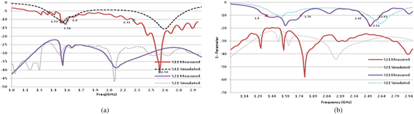
When both PIN diodes are in ON state antenna resonates at 1.41–1.52 GHz with bandwidth 140 MHz and at frequency 2.29–2.62 GHz with bandwidth 330 MHz. The measured and simulated values of S-parameter for different biasing conditions of PIN diodes are also plotted on Figs 11(a) and 11(b). The value S 11 when both the diodes are ON is −13.35 and −17.07 dB at 1.5 and 2.5 GHz, respectively. The VSWR is measured to be 1.56 when both the diodes are in ON condition.
Measured and simulated S- parameter of MIMO antenna (a) when bo1h PIN diodes are ON (b) when both PIN dioies 1 is ON and Diode 2 is OFF

These results show reasonable agreement although there is a frequency shift, which may be because of reflections from the SMA connector and some ambiguity in the electrical properties of the substrate material. It is observed that the bandwidth increases for different biasing conditions of PIN diodes. To sum up, the proposed antenna is dual band MIMO antenna with circular polarization, the impedance of 50 Ω, VSWR ≤ 1.8 with envelope correlation coefficient of 0.001–0.004 with improved bandwidth used for an application like Wi-Fi, GPS, router, and vehicular communication.
V. CONCLUSION
A novel frequency reconfigurable dual-band MIMO antenna with pentagon slot resonator has been presented. This antenna design achieves circular polarization with reconfigurability of frequency. Two PIN diodes are embedded to increase the current flow. This gives enhancement of bandwidth within the frequency range. The MIMO antenna array provides better envelope correlation of <0.004 and stable bidirectional patterns and good isolation of <20 dB. Finally, it is concluded that with this novel antenna can be used for vehicular communication like trains GPS system on elevated railways and for multimode application where wideband is required and for GPS, Wi-Fi technology, etc.
 Mrs. Deepali K. Borakhade is working as Assistant Professor at St. Vincent College of Engineering and Technology, Nagpur, Maharashtra, India. She has done her masters in Digital Electronics and is doing her Ph.D. work on frequency reconfigurable antenna from Shri Ramdeobaba College of Engineering and Management, Nagpur, under Nagpur University.
 Dr. Sanjay B. Pokle received the B.E. degree in Electronics & Telecommunication Engineering. From Govt. College of Engineering, Pune and completed his M.Tech., Ph.D. degrees in Electronics from Visvesvaraya National Institute of Technology, Nagpur. His present field of research interest is Digital Signal Processing & its applications and Wireless Communication. He is working as a Professor & Head in the Department of Electronics & Communication Engineering, Shri Ramdeobaba College of Engineering & Management, Nagpur. He is an IEEE and ISTE life member. He received many appreciation certificates in many research paper publications.